


The Role of III-V Substrate Roughness and Deoxidation Induced by Digital Etch in Achieving Low Resistance Metal Contacts

Abstract
1. Introduction
2. Materials and Methods
3. Results and Discussion
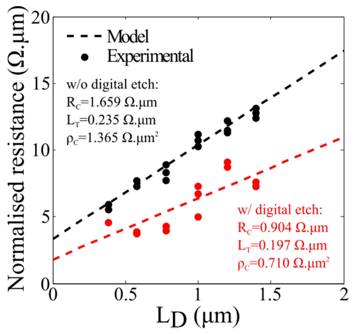
3.1. Resistivity
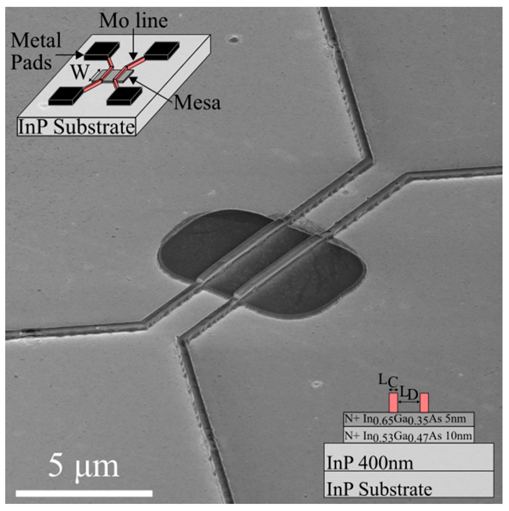
3.2. Device Conformity
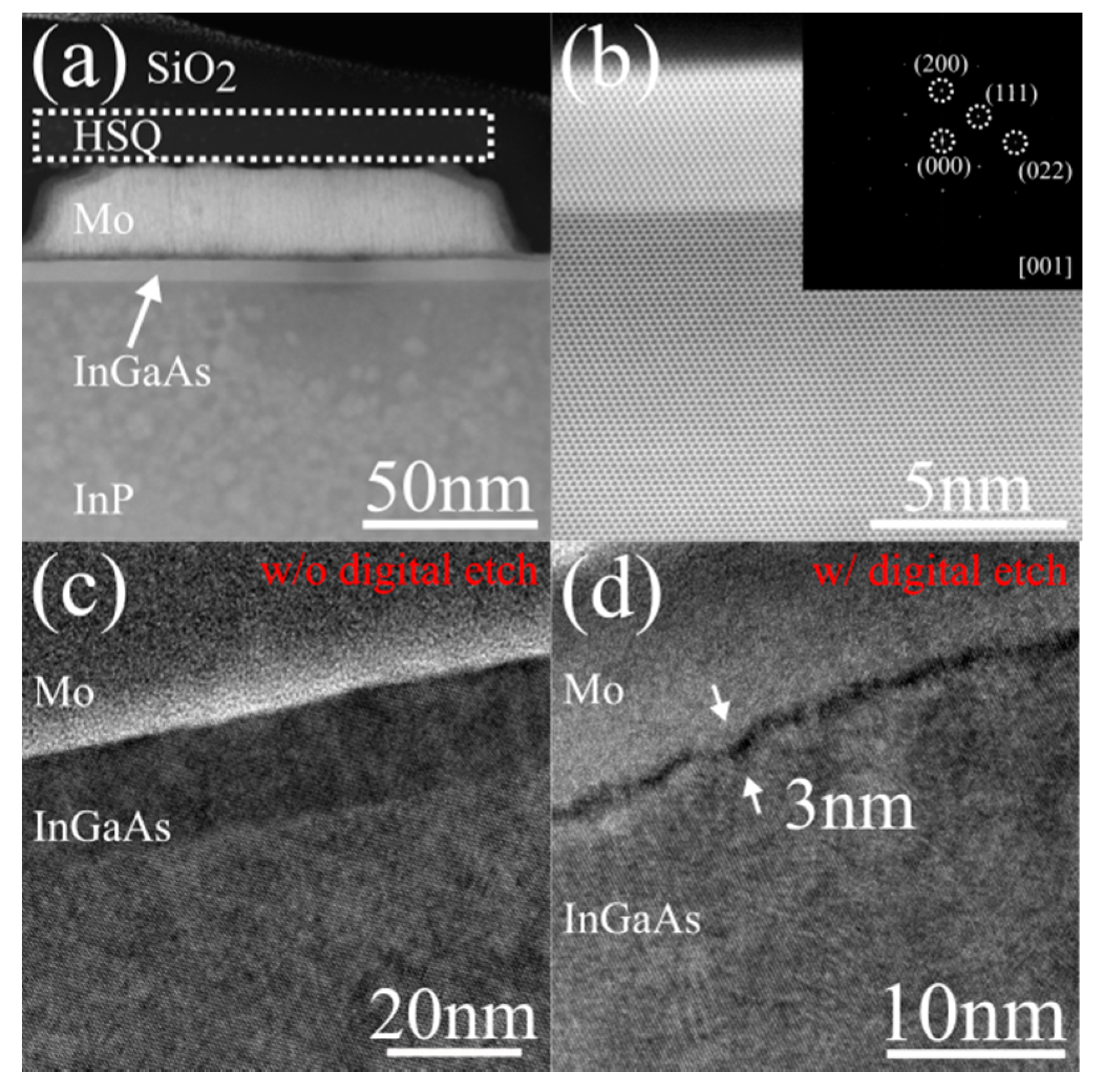
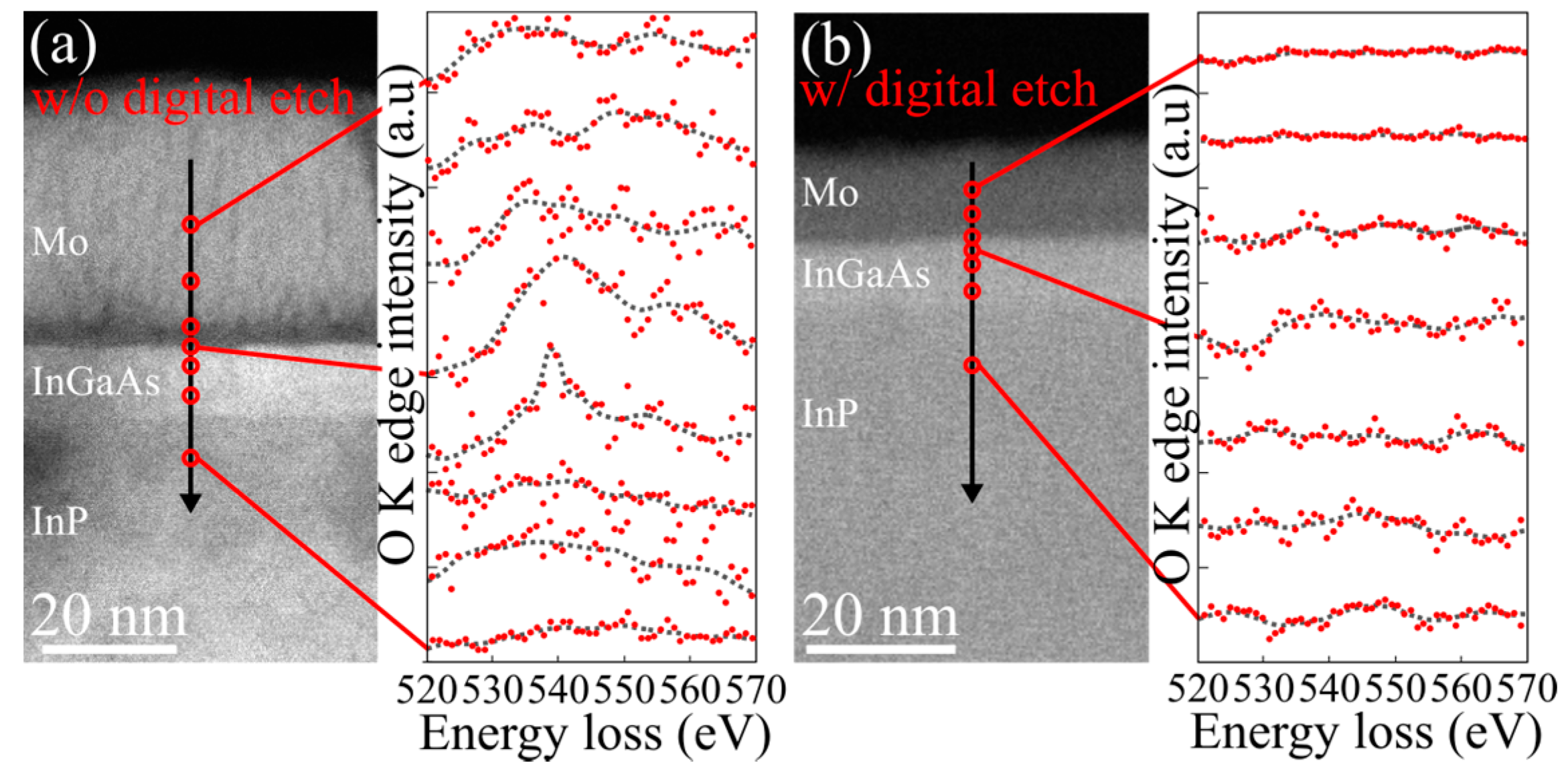
3.3. Interface Probing
4. Conclusions
Acknowledgments
Author Contributions
Conflicts of Interest
References
- Skotnicki, T.; Hutchby, J.A.; King, T.; Wong, H.S.P.; Boeuf, F. The end of CMOS scaling : Toward the introduction of new materials and structural changes to improve MOSFET performance. IEEE Circuits Devices Mag. 2005, 21, 16–26. [Google Scholar] [CrossRef] [Scilit]
- Del Alamo, J.A. Nanometre-scale electronics with III-V compound semiconductors. Nature 2011, 479, 317–323. [Google Scholar] [CrossRef] [Scilit] [PubMed]
- Hu, C.Y.; Hashizume, T.; Ohi, K.; Tajima, M. Trapping effect evaluation of gateless AlGaN/GaN heterojunction field-effect transistors using transmission-line-model method. Appl. Phys. Lett. 2010, 97, 222103. [Google Scholar] [CrossRef] [Scilit]
- Kim, S.H.; Yokoyama, M.; Taoka, N.; Iida, R.; Lee, S.; Nakane, R.; Urabe, Y.; Miyata, N.; Yasuda, T.; Yamada, H.; et al. Self-aligned metal source/drain InxGa1-xAs n-MOSFETs using Ni-InGaAs alloy. In Proceedings of the IEEE International Electron Devices Meeting (IEDM), San Francisco, CA, USA, 6–8 December 2010; pp. 596–599. [Google Scholar]
- Zhang, X.; Guo, H.; Ko, C.H.; Wann, C.H.; Cheng, C.C.; Lin, H.Y.; Chin, H.C.; Gong, X.; Lim, P.S.Y.; Luo, G.L.; et al. III-V MOSFETs with a new self-aligned contact. In Proceedings of the 2010 Symposium on VLSI Technology, Honolulu, HI, USA, 15–17 June 2010; pp. 233–234. [Google Scholar]
- Yuan, Z.; Kumar, A.; Chen, C.Y.; Nainani, A.; Bennett, B.R.; Boos, J.B.; Saraswat, K.C. Antimonide-Based Heterostructure p-Channel MOSFETs with Ni-Alloy Source/Drain. IEEE Electron Device Lett. 2013, 34, 1367–1369. [Google Scholar] [CrossRef]
- Zhang, X.; Guo, H.X.; Zhu, Z.; Gong, X.; Yeo, Y.C. In0.53Ga0.47As FinFETs with self-aligned molybdenum contacts and HfO2/Al2O3 gate dielectric. Solid State Electron. 2013, 84, 83–89. [Google Scholar] [CrossRef] [Scilit]
- Lee, R.T.P.; Loh, W.Y.; Tieckelmann, R.; Orzali, T.; Huffman, C.; Vert, A.; Huang, G.; Kelman, M.; Karim, Z.; Hobbs, C.; et al. Technology Options to Reduce Contact Resistance in Nanoscale III-V MOSFETs. ECS Trans. 2015, 66, 125–134. [Google Scholar] [CrossRef] [Scilit]
- Liao, M.H.; Chen, P.K. Experimental demonstration on the ultra-low source/drain resistance by metal-insulator-semiconductor contact structure in In0.53Ga0.47As field-effect transistors. AIP Adv. 2013, 3, 092118. [Google Scholar] [CrossRef] [Scilit]
- Law, J.J.M.; Carter, A.D.; Lee, S.; Huang, C.Y.; Lub, H.; Rodwell, M.J.W.; Gossard, A.C. Co-doping of InxGa1-xAs with silicon and tellurium for improved ultra-low contact resistance. J. Cryst. Growth 2013, 378, 92–95. [Google Scholar] [CrossRef] [Scilit]
- Jones, K.S.; Lind, A.G.; Hatem, C.; Moffatt, S.; Ridgeway, M.C. A Brief Review of Doping Issues in III-V Semiconductors. ECS Trans. 2013, 53, 97–105. [Google Scholar] [CrossRef] [Scilit]
- Barnett, J.; Hill, R.; Loh, W.Y.; Hobbs, C.; Majhi, P.; Jammy, R. Advanced techniques for achieving ultra-shallow junctions in future CMOS devices. In Proceedings of the 2010 International Workshop on Junction Technology, Shanghai, China, 10–11 May 2010; pp. 1–4. [Google Scholar]
- Orzali, T.; Vert, A.; Lee, R.T.P.; Norvilas, A.; Huang, G.; Herman, J.L.; Hill, R.J.W.; Papa Rao, S.S. Heavily tellurium doped n-type InGaAs grown by MOCVD on 300 mm Si wafers. J. Cryst. Growth 2007, 426, 243–247. [Google Scholar] [CrossRef] [Scilit]
- Athavalea, S.D.; Economoub, D.J. Realization of atomic layer etching of silicon. J. Vac. Sci. Technol. B 1996, 14, 3702–3805. [Google Scholar] [CrossRef] [Scilit]
- Ko, K.K.; Pang, S.W. Controllable layer-by-layer etching of III–V compound semiconductors with an electron cyclotron resonance source. J. Vac. Sci. Technol. B 1993, 11, 2275–2279. [Google Scholar] [CrossRef] [Scilit]
- Lin, J.; Zhao, X.; Yu, T.; Antoniadis, D.A.; del Alamo, J.A. A new self-aligned quantum-well MOSFET architecture fabricated by a scalable tight pitch process. In Proceedings of the 2013 IEEE International Electron Devices Meeting (IEDM), Washington, DC, USA, 9–11 December 2013; pp. 421–424. [Google Scholar]
- DeSalvo, G.C.; Bozada, C.A.; Ebel, J.L.; Look, D.C.; Barrette, J.P.; Cerny, C.L.A.; Dettmer, R.W.; Gillespie, J.K.; Havasy, C.K.; Jenkins, T.J.; et al. Wet Chemical Digital Etching of GaAs at Room Temperature. J. Electrochem. Soc. 1996, 143, 3652–3656. [Google Scholar] [CrossRef] [Scilit]
- Alian, A.; Merckling, C.; Brammertz, G.; Meuris, M.; Heyns, M.; De Meyer, K. InGaAs MOS transistors fabricated through a digital-etch gate-recess process and the influence of forming gas anneal on their electrical behavior. ECS J. Solid State Sci. Technol. 2012, 6, 310–314. [Google Scholar] [CrossRef] [Scilit]
- Lin, J.; Zhao, X.; Antoniadis, D.A.; del Alamo, J.A. A Novel Digital Etch Technique for Deeply Scaled III-V MOSFETs. IEEE Electron Device Lett. 2014, 35, 440–442. [Google Scholar] [CrossRef] [Scilit]
- Rajput, N.S.; Kim, S.G.; Chou, J.B.; Abed, J.; Viegas, J.; Jouiad, M. Electron beam induced rapid crystallization of water splitting nanostructures. MRS Adv. 2015, 1, 825–830. [Google Scholar] [CrossRef] [Scilit]
- Ravaux, F.; Alnuaimi, K.S.; Jouiad, M.; Saadat, I. Characterization of metal contact to III–V materials (Mo/InGaAs). Microelectron. Eng. 2015, 145, 1–4. [Google Scholar] [CrossRef] [Scilit]
- Lu, W.; Guo, A.; Vardi, A.; del Alamo, J.A. A Test Structure to Characterize Nano-Scale Ohmic Contacts in III-V MOSFETs. IEEE Electron Device Lett. 2014, 35, 178–180. [Google Scholar] [CrossRef] [Scilit]
- Buttari, D.; Heikman, S.; Keller, S.; Mishra, U.K. Digital Etching for Highly Reproducible Low Damage Gate Recessing on AlGaN/GaN HEMTs. In Proceedings of the 2002 IEEE Lester Eastman Conference, Newark, DE, USA, 8 August 2002; pp. 461–469. [Google Scholar]
- Muller, D.A.; Sorsch, T.; Moccio, S.; Baumann, F.H.; Evans-Lutterodt, K.; Timp, G. The electronic structure at the atomic scale of ultrathin gate oxides. Nature 1999, 399, 758–761. [Google Scholar] [CrossRef] [Scilit]
- Verleysen, E.; Bender, H.; Richard, O.; Schryvers, D.; Vandervorst, W. Characterization of nickel silicides using EELS-based methods. J. Microsc. 2010, 240, 75–82. [Google Scholar] [CrossRef] [Scilit] [PubMed]
- Hussey, R.J.; Sproule, G.I.; McCaffrey, J.P.; Graham, M.J. Characterization of Oxides Formed on InP, InGaAs, InAlAs, and InGaAs/InAlAs Heterostructures at 300–500 °C. Oxid. Met. 2002, 57, 427–447. [Google Scholar] [CrossRef] [Scilit]
- Brennan, B.; Hughes, G. Identification and thermal stability of the native oxides on InGaAs using synchrotron radiation based photoemission. J. Appl. Phys. 2010, 108, 053516. [Google Scholar] [CrossRef] [Scilit]
© 2017 by the authors. Licensee MDPI, Basel, Switzerland. This article is an open access article distributed under the terms and conditions of the Creative Commons Attribution (CC BY) license (http://creativecommons.org/licenses/by/4.0/).
Share and Cite
Ravaux, F.; Saadat, I.; Jouiad, M. The Role of III-V Substrate Roughness and Deoxidation Induced by Digital Etch in Achieving Low Resistance Metal Contacts. Crystals 2017, 7, 177. https://doi.org/10.3390/cryst7060177
Ravaux F, Saadat I, Jouiad M. The Role of III-V Substrate Roughness and Deoxidation Induced by Digital Etch in Achieving Low Resistance Metal Contacts. Crystals. 2017; 7(6):177. https://doi.org/10.3390/cryst7060177
Chicago/Turabian StyleRavaux, Florent, Irfan Saadat, and Mustapha Jouiad. 2017. "The Role of III-V Substrate Roughness and Deoxidation Induced by Digital Etch in Achieving Low Resistance Metal Contacts" Crystals 7, no. 6: 177. https://doi.org/10.3390/cryst7060177
APA StyleRavaux, F., Saadat, I., & Jouiad, M. (2017). The Role of III-V Substrate Roughness and Deoxidation Induced by Digital Etch in Achieving Low Resistance Metal Contacts. Crystals, 7(6), 177. https://doi.org/10.3390/cryst7060177