A Study on Graphene—Metal Contact

Abstract
:1. Introduction
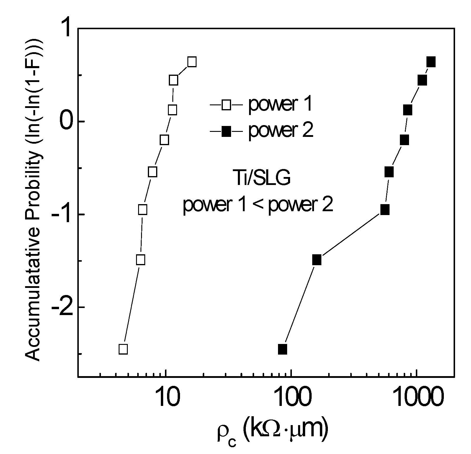
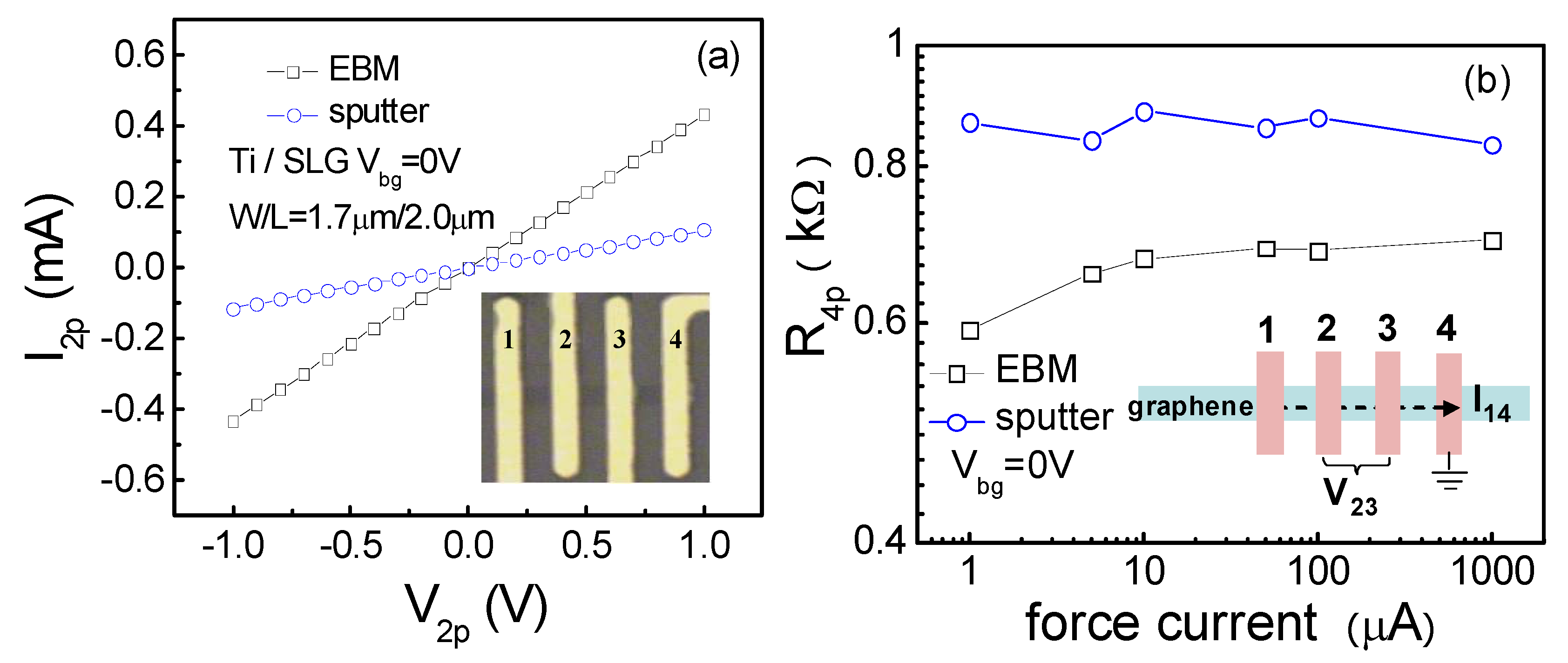
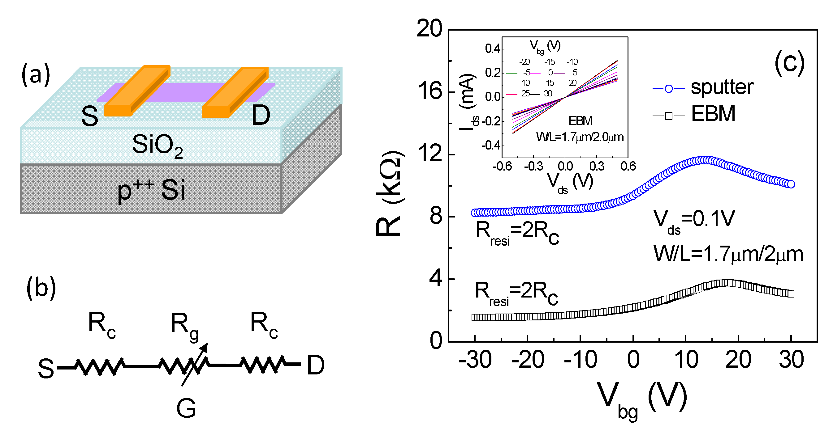
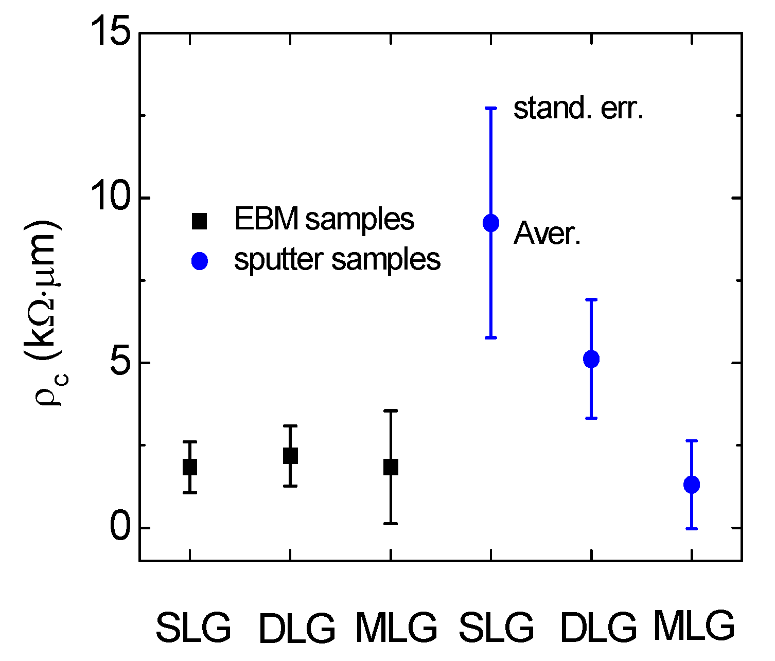
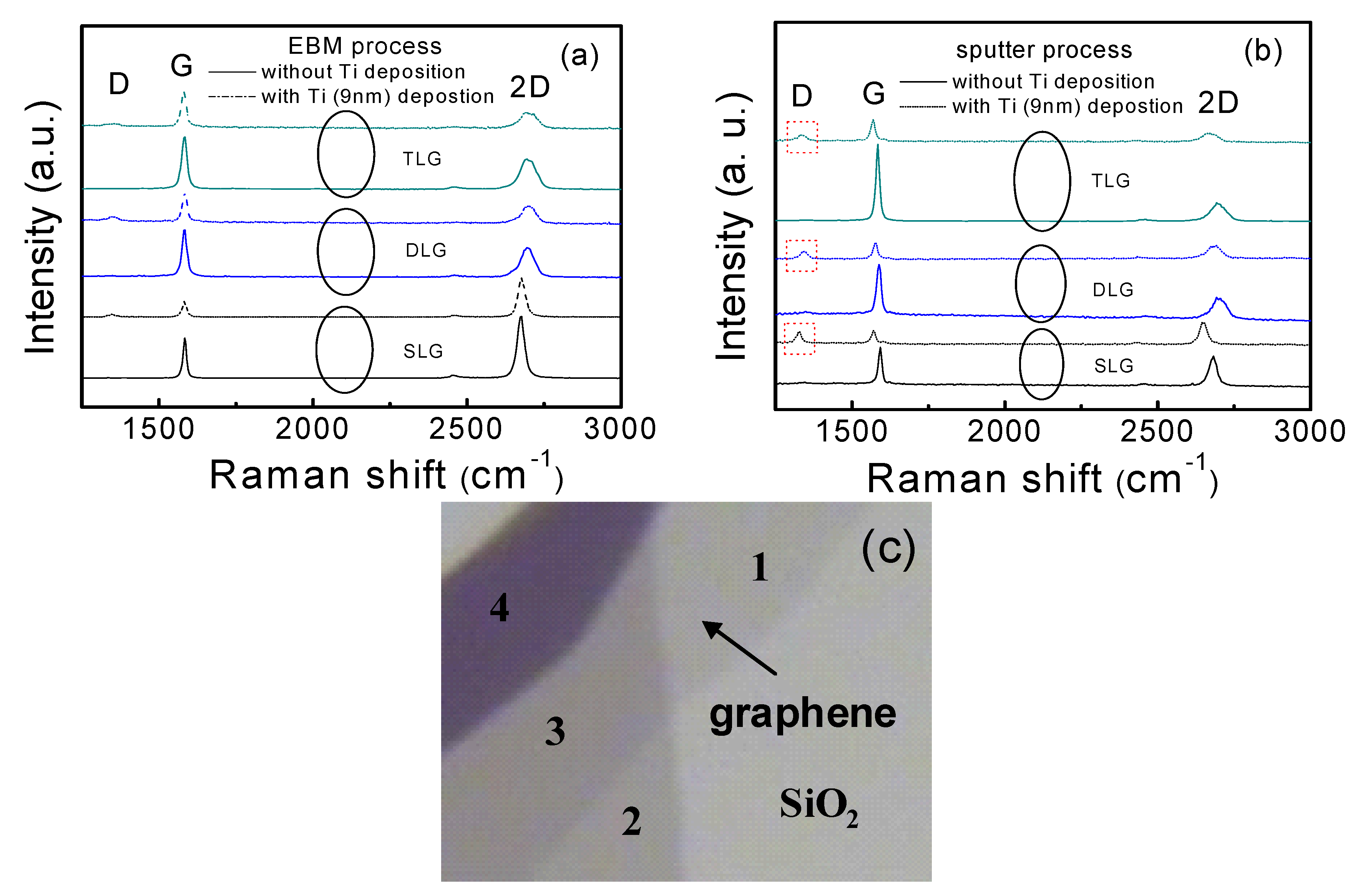
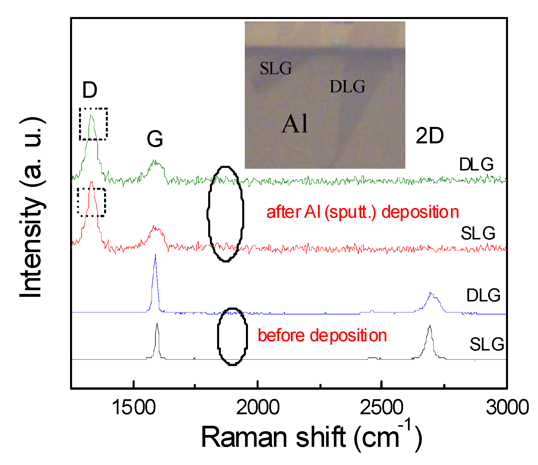
2. Impact of Metal Preparation


3. Asymmetry Conductance
 [47], where N(EF) is the DOS at the EF in graphene. The λ is less than 1 nm for metal–metal contact. However, for graphene–metal contact, DOS is very small compared to metal, especially at the Dirac point, and λ is much larger than that of metal. In addition, graphene itself is sensitive to external perturbations owing to its all-surface and zero volume nature [48]. Charge transfer between graphene and metal may dope the underlying graphene into n-type or p-type, depending on work function differences. Therefore, the metal doping effect must be considered in transfer characteristics of graphene FETs. In Figure 2, it is shown that p-type and n-type branches show a moderate asymmetry and the conductance in the n-type branch is always smaller than that in the p branch. It is consistent with the previous report [18]. This asymmetric conductance behavior was first investigated by comparing devices with invasive electrodes crossing the whole graphene channel width and external electrodes connected to the side of the graphene channel [23]. The graphene FETs with invasive electrode show the asymmetry of conductance in n-type and p-type branches; however, the asymmetry almost never occurs in devices with external electrodes [18,23]. Giovannetti and Khomyakov et al. [49,50] applied density functional theory (DFT) to study how graphene is doped by various metals, including Al, Ag, Cu, Au, Pt. The calculated Fermi energy shift (∆EF) with respect to the conical point can increase by decreasing the distance between graphene and metal. Xia et al., by using scanning photocurrent microscopy (SPCM), illustrated that the charge doping occurs not only underneath the metal, but also extends hundreds of nanometers into adjacent regions in the graphene channel [51,52]. They separated a graphene FET into three segments: (1) the metal-controlled graphene; (2) the transition region affected by both the metal and the back-gate; and (3) the bulk graphene region controlled only by the back-gate. With the modulation of back-gate voltage, the width of transition region (segment 2) is accordingly modified. In their experiments, the detected photocurrent comes from the p–n junction in the graphene sheet, since the photocurrent is proportional to the potential gradient at the excitation position. It exhibits the different polarities along the graphene channel. Lee et al. [53] observed the photocurrent in graphene FETs with the help of SPCM, resulting from p–n junction formation in the graphene sheet. It was also reported that chemical doping can introduce conductance asymmetry. It is caused by a combination of the neutrality point misalignment at the electrode–channel interface and the non-constant DOS of the graphene electrodes [54].
 is the Plank constant divided by 2π;
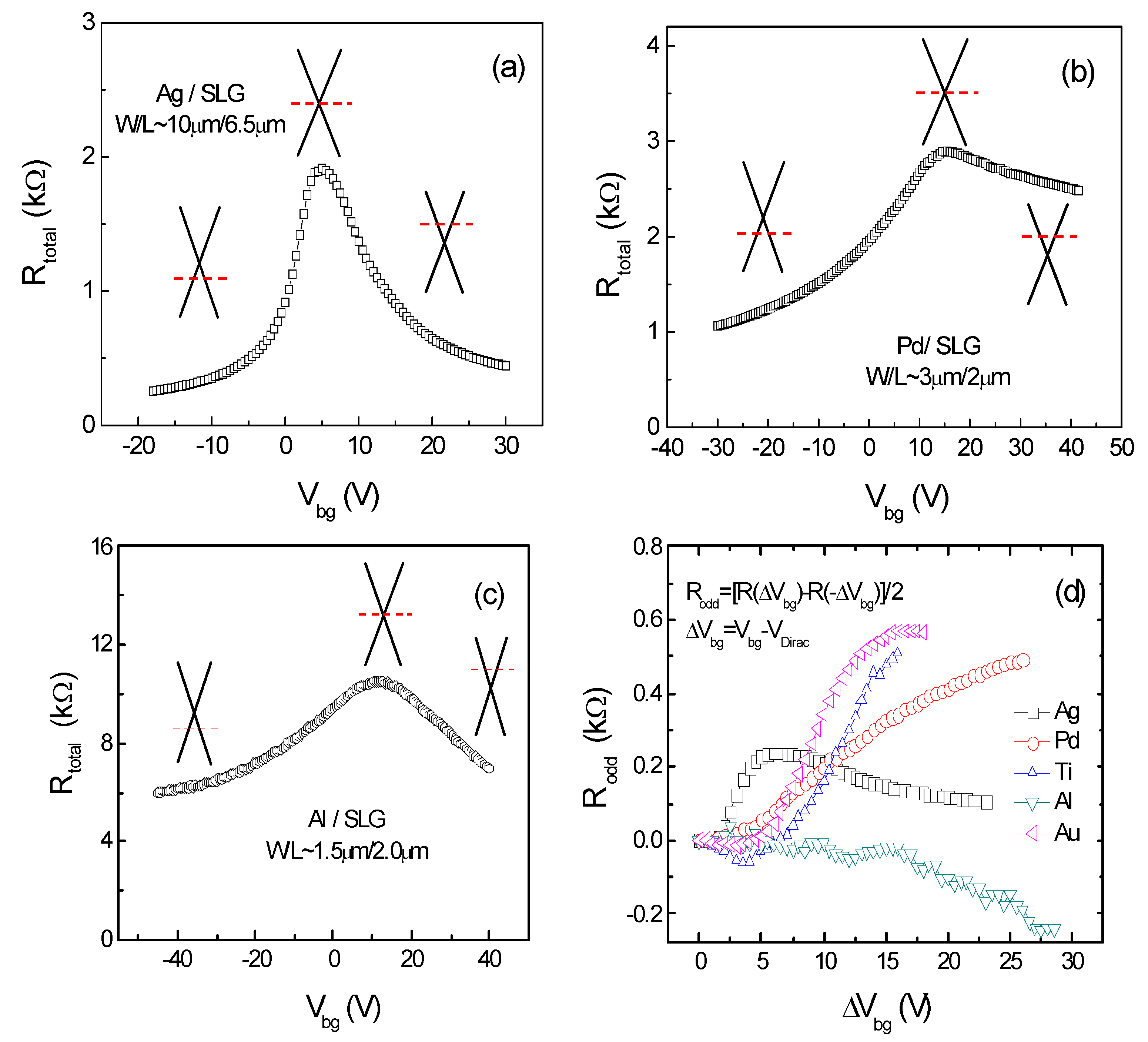
  is the flat band voltage; νF is Fermi velocity of 0.8 × 10⁶ m/s; α is 2.24 × 10 11cm−2v−1, which is estimated from a simple capacitor model [56]. The results show that the effective constant potential ∆ϕ for Ti/SLG, Al/SLG, Ag/SLG Pd/SLG is 0.1 eV, −0.22 eV, 0.08 eV, 0.45 eV, respectively. For Ti/SLG, our calculated ∆ϕ is consistent with Xia’s report of ~0.12 eV [51] or 0.1 eV [52], Figure 7a–c shows the Rtotal − Vbg plots of graphene FETs with different metal electrodes Ag, Pd, Al, respectively. They exhibit an asymmetric behavior in hole and electron transportation branches, including the graphene FETs with Ti electrode, shown in Figure 2. The numerical simulation has shown that the Fermi level of graphene underneath the metal is shifted and may result in asymmetric transfer characteristics [57], which is similar to the aforementioned. The odd resistance is used to characterize the asymmetry in graphene FETs with various metal electrodes. The Rodd is defined as follows [23,52]:

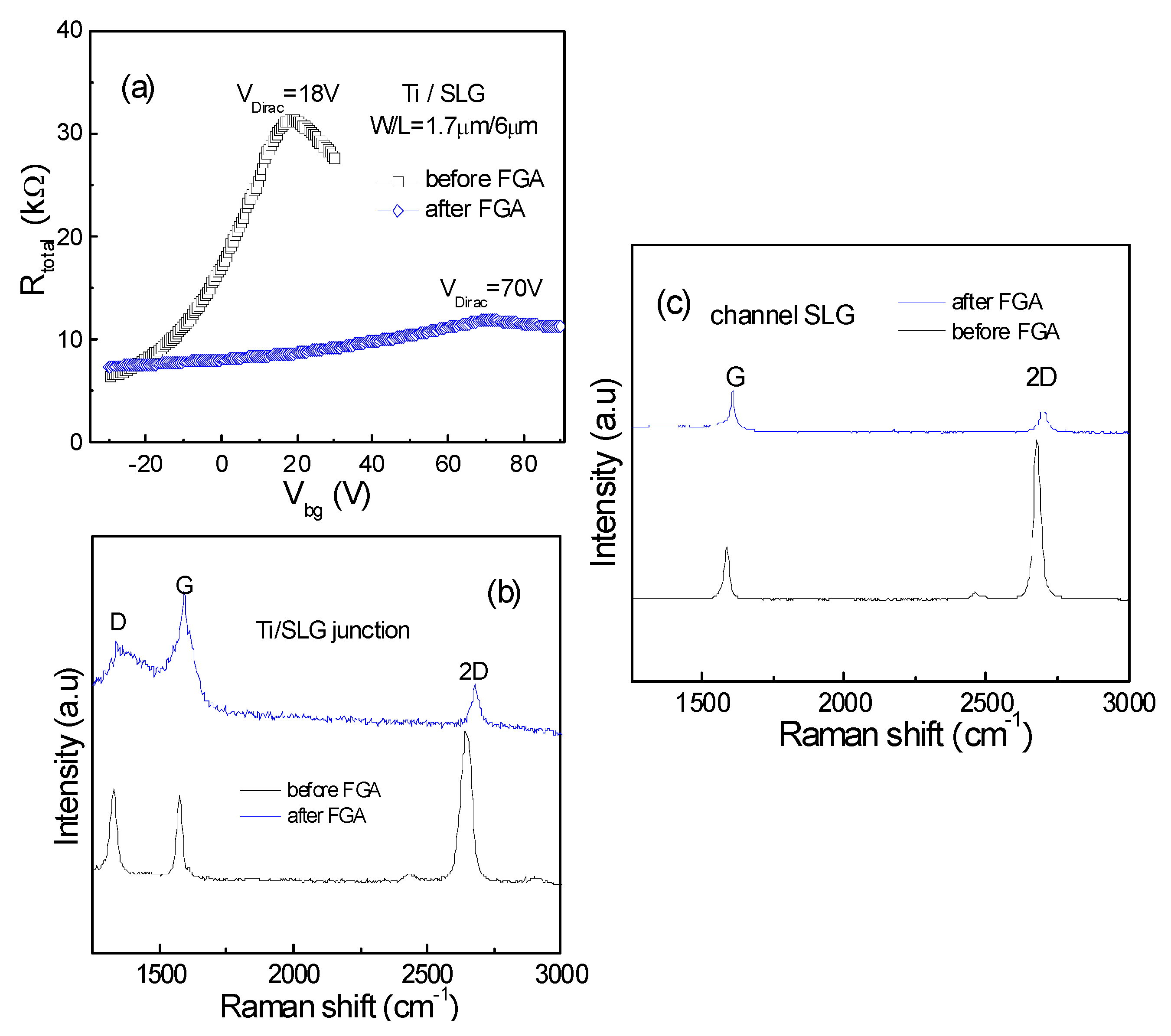
4. Annealing Effect on Contact Junction

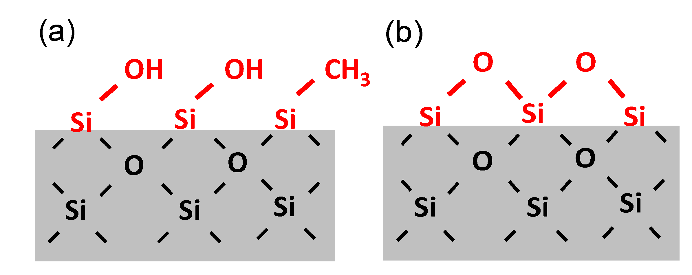
5. Interface Impact
6. Conclusions
Acknowledgments
Conflict of Interest
References
- Novoselov, K.S.; Geim, A.K.; Morozov, S.V.; Jiang, D.; Zhang, Y.; Dubonos, S.V.; Grigorieva, I.V.; Firsov, A.A. Electric field effect in atomically thin carbon films. Science 2004, 306, 666–669. [Google Scholar] [CrossRef]
- Zhang, Y.; Tan, Y.W.; Stormer, H.L.; Kim, P. Experimental observation of the quantum hall effect and Berry’s phase in graphene. Nature 2005, 438, 201–204. [Google Scholar]
- Geim, A.K.; Novoselov, K.S. The rise of graphene. Nat. Mater. 2007, 6, 183–191. [Google Scholar] [CrossRef]
- Chen, Z.; Lin, Y.M.; Rooks, M.J.; Avouris, Ph. Graphene nano-ribbon electronics. Phys. E 2007, 40, 228–232. [Google Scholar] [CrossRef]
- Schedin, F.; Geim, A.; Morozov, S.V.; Hill, E.W.; Blake, P.; Katsnelson, M.I.; Novoselov, K.S. Detection of individual gas molecules adsorbed on graphene. Nat. Mater. 2007, 6, 652–655. [Google Scholar] [CrossRef]
- Lemme, M.C.; Echtermeyer, T.J.; Baus, M.; Kurz, H. A graphene field-effect device. IEEEElectron. Dev. Lett. 2007, 28, 282–284. [Google Scholar] [CrossRef]
- Murali, R.; Yang, Y.X.; Brenner, K.; Beck, T.; James, D.M. Breakdown current density of graphene nanoribbons. Appl. Phys. Lett. 2009, 94, 243114:1–243114:3. [Google Scholar]
- Li, X.; Wang, X.; Zhang, L.; Lee, S.; Dai, H. Chemically derived, ultrasmooth graphene nanoribbon semiconductors. Science 2008, 319, 1229–1232. [Google Scholar] [CrossRef]
- Castro Neto, A.H.; Guinea, F.; Peres, N.M.R.; Novoselov, K.S.; Geim, A.K. The electronic properties of graphene. The electronic properties of graphene. Rev. Mod. Phys. 2009, 81, 109–162. [Google Scholar]
- Lin, Y.M.; Dimitrakopoulos, C.; Jenkins, K.A.; Farmer, D.B.; Chiu, H.Y.; Grill, A.; Avouris, Ph. 100-GHz transistors from wafer-scale epitaxial graphene. Science 2010, 327, 662. [Google Scholar] [CrossRef]
- Schwierz, F. Graphene transistors. Nat. Nanotechnol. 2010, 5, 487–496. [Google Scholar] [CrossRef]
- Bolotin, K.I.; Sikes, K.J.; Jiang, Z.; Fundenberg, G.; Hone, J.; Kim, P.; Stormer, H.L. Ultrahigh electron mobility in suspended graphene. Solid State Commun. 2008, 146, 351–355. [Google Scholar]
- Fan, X.Y.; Nouchi, R.; Yin, L.C.; Tanigaki, K. Effects of electron-transfer chemical modification on the electrical characteristics of graphene. Nanotechnology 2010, 21, 475208:1–475208:5. [Google Scholar]
- Hong, S.K.; Kim, J.E.; Kim, S.O.; Choi, S.Y.; Cho, B.J. Flexible resistive switching memory device based on graphene oxide. IEEE Electron. Dev. Lett. 2010, 31, 1005–1007. [Google Scholar] [CrossRef]
- Jeong, H.Y.; Yun, J.; Kim, J.Y.; Hwang, J.O.; Kim, J.E.; Lee, J.Y.; Yoon, T.H.; Cho, B.J.; Kim, S.O.; Ruoff, R.S.; et al. Graphene oxide thin films for flexiblenonvolatile memory applications. Nano Lett. 2010, 10, 4381–4386. [Google Scholar] [CrossRef]
- Eda, G.; Lin, Y.Y.; Miller, S.; Chen, C.W.; Su, W.F.; Chhowalla, M. Transparent and conducting electrodes for organic electronics from reduced graphene oxide. Appl. Phys. Lett. 2008, 92, 233305:1–233305:3. [Google Scholar]
- Yan, X.; Cui, X.; Li, B.; Li, L.S. Large, solution-processable graphene quantum dots as light absorbers for photovoltaics. Nano Lett. 2010, 10, 1869–1873. [Google Scholar] [CrossRef]
- Nagashio, K.; Nishimura, T.; Kita, K.; Toriumi, A. Metal/Graphene Contact as a Performance Killer of Ultra-high Mobility Graphene—Analysis of Intrinsic Mobility and Contact Resistance. In Presented at the International Electron Devices Meeting, Washington DC, USA, 7–9 December 2009.
- Nagashio, K.; Nishimura, T.; Kita, K.; Toriumi, A. Contact resistivity and current flow path at metal/graphene contact. Appl. Phys. Lett. 2010, 97, 143514:1–143514:3. [Google Scholar]
- Venugopal, A.; Colombo, L.; Vogel, E.M. Contact resistance in few and multilayer graphene devices. Appl. Phys. Lett. 2010, 96, 013512:1–013512:3. [Google Scholar]
- Xia, F.; Perebeions, V.; Lin, Y.M.; Wu, Y.Q.; Avouris, Ph. The origins and limits of metal graphene junction resistance. Nat. Nanotechnol. 2011, 6, 179–184. [Google Scholar]
- Watanabe, E.; Conwill, A.; Tsuya, D.; Koide, Y. Low contact resistance metals for graphene based devices. Diam. Relat. Mater. 2012, 24, 171–174. [Google Scholar] [CrossRef]
- Huard, B.; Stander, N.; Sulpizio, J.A.; Goldhber-Gordon, D. Evidence of the role of contacts on the observed electron-hole asymmetry in graphene. Phys. Rev. B 2008, 78, 121402:1–121402:4. [Google Scholar]
- Liu, W.; Li, M.; Xu, S.; Zhang, Q.; Pey, K.L.; Hu, H.; Shen, Z.; Zou, X.; Wang, J.; Wei, J.; et al. Understanding the Contact Characteristics in Single or Multi-Layer Graphene Devices: The Impact of Defects (Carbon Vacancies) and the Asymmetric Transportation Behavior. In Presented at the International Electron Devices Meeting, San Francisco, CA, USA, 6–8 December 2010.
- Dai, H. Carbon nanotubes: Opportunities and challenges. Surf. Sci. 2002, 500, 218–241. [Google Scholar] [CrossRef]
- Blake, P.; Yanga, R.; Morozova, S.V.; Schedin, F.; Ponomarenkoa, L.A.; Zhukova, A.A.; Nair, R.R.; Grigorieva, I.V.; Novoselov, K.S.; Geim, A.K. Influence of metal contacts and charge inhomogeneity on transport properties of graphene near the neutrality point. Solid State Commun. 2009, 149, 1068–1071. [Google Scholar] [CrossRef]
- Liu, W.J.; Yu, H.Y.; Wei, J.; Li, M.F. Impact of process induced defects on the contact characteristics of ti/graphene devices. Electrochem. Solid State Lett. 2011, 14, K67–K69. [Google Scholar] [CrossRef]
- Magna, L.; Deretzis, I. Theoretical study of the role of metallic contacts in probing transport features of pure and defected graphene nanoribbons. Nanoscale. Res. Lett. 2011, 6, 234:1–234:5. [Google Scholar]
- Seol, G.; Guo, J. Metal contact to graphene nanoribbon. Appl. Phy. Lett. 2012, 100, 063108:1–063108:4. [Google Scholar]
- Russo, S.; Craciun, M.F.; Yamamoto, M.; Morpurgo, A.F.; Tarucha, S. Contact resistance in graphene-based devices. Physica E 2010, 42, 677–679. [Google Scholar] [CrossRef]
- Pimenta, M.A.; Dresselhaus, G.; Dresselhaus, M.S.; Cancado, L.G.; Jorioa, A.; Saitoe, R. Studying disorder in graphite-based systems by Raman spectroscopy. Phys. Chem. Chem. Phys. 2007, 9, 1276–1291. [Google Scholar] [CrossRef]
- Ferrari, A.C.; Meyer, J.C.; Scardaci, V.; Casiraghi, C.; Lazzeri, M.; Mauri, F.; Piscanec, S.; Jiang, D.; Novoselov, K.S.; Roth, S.; et al. Raman spectrum of graphene and graphene layers. Phys. Rev. Lett. 2006, 97, 187401:1–187401:4. [Google Scholar]
- Ni, Z.H.; Wang, H.M.; Kasim, J.; Fan, H.M.; Yu, T.; Wu, Y.H.; Peng, Y.P.; Shen, Z.X. Graphene thickness determination using reflection and contrast spectroscopy. Nano Lett. 2007, 7, 2758–2763. [Google Scholar] [CrossRef]
- Wang, Y.Y.; Ni, Z.H.; Yu, T.; Shen, Z.X.; Wang, H.M.; Wu, Y.H.; Chen, W.; Wee, A. Raman studies of monolayer graphene: The substrate effect. J. Phys. Chem. C 2008, 112, 10637–10640. [Google Scholar]
- Ni, Z.H.; Wang, H.M.; Ma, Y.; Kasim, J.; Wu, Y.H.; Shen, Z.X. tunable stress and controlled thickness modification in graphene by annealing. ACS Nano 2008, 2, 1033–1039. [Google Scholar] [CrossRef]
- Liu, W.; Tran, X.; Liu, X.; Wei, J.; Yu, H.; Sun, X. Characteristics of a single-layer graphene field effect transistor with UV/Ozone treatment. Electrochem. Solid State Lett. 2013, 2, M1–M4. [Google Scholar]
- Xu, C.H.; Fu, C.L.; Pedraza, D.F. Simulation of point-defect properties in graphite by a tight-binding-force model. Phys. Rev. B 1993, 48, 13273–13279. [Google Scholar] [CrossRef]
- El-Barbary, A.; Telling, R.H.; Ewels, C.P.; Heggie, M.I.; Briddon, P.R. Structure and energetics of the vacancy in graphite. Phys. Rev. B 2003, 68, 144107:1–144107:7. [Google Scholar]
- Yan, J.; Zhang, Y.B.; Kim, P.; Pinczuk, A. Electric field effect tuning of electron-phonon coupling in graphene. Phys. Rev. Lett. 2007, 98, 166802:1–166802:4. [Google Scholar]
- Ni, Z.; Yu, T.; Luo, Z.; Wang, Y.; Liu, L.; Wong, C.; Miao, J.; Huang, W.; Shen, Z. Probing charged impurities in suspended graphene using raman spectroscopy. ACS Nano 2009, 3, 569–574. [Google Scholar] [CrossRef]
- Mohiuddin, T.M.G.; Lombardo, A.; Nair, R.R.; Bonetti, A.; Savini, G.; Jalil, R.; Bonini, N.; Basko, D.M.; Gailiotis, C.; Marzari, N.; et al. Uniaxial strain in graphene by Raman spectroscopy: G peak splitting, Grüneisen parameters, and sample orientation. Phy. Rev. B 2009, 79, 205433:1–205433:8. [Google Scholar]
- Ni, Z.H.; Yu, T.; Lu, Y.H.; Wang, Y.Y.; Feng, Y.P.; Shen, Z.X. Uniaxial strain on graphene: Raman spectroscopy study and band-gap opening. ACS Nano 2008, 2, 2301–2305. [Google Scholar] [CrossRef]
- Chen, J.H.; Cullen, W.G.; Jang, C.; Fuhrer, M.S.; Williams, E.D. Defect scattering in graphene. Phys. Rev. Lett. 2009, 102, 236805:1–236805:4. [Google Scholar]
- Ni, Z.H.; Ponomarenko, L.A.; Nair, R.R.; Yang, R.; Anissimova, S.; Grigorieva, I.V.; Schedin, F.; Blake, P.; Shen, Z.X.; Hill, E.H.; et al. On resonant scatterers as a factor limitingcarrier mobility in graphene. Nano Lett. 2010, 10, 3868–3872. [Google Scholar] [CrossRef]
- Lahiri, J.; Batzilla, M. Graphene destruction by metal-carbide formation: An approach for patterning of metal-supported graphene. Appl. Phys. Lett. 2010, 97, 023102:1–023102:3. [Google Scholar]
- Li, H.; Zhang, Q.; Liu, C.; Xu, S.H.; Gao, P.Q. Ambipolar to unipolar conversion in graphene field-effect transistors. ACS Nano 2011, 5, 3198–3203. [Google Scholar] [CrossRef]
- Nagashio, K.; Toriumi, A. Density-of-states limited contact resistance in graphene field-effect transistors. Jpn. J. Appl. Phys. 2011, 50, 070108:1–070108:6. [Google Scholar]
- Berdebes, D.; Low, T.; Sui, Y.; Appenzeller, J.; Lundstrom, M.S. Substrate gating of contact resistance in graphene transistors. IEEE Trans. Electron. Dev. 2011, 58, 3925–3932. [Google Scholar]
- Giovannetti, G.; Khomyakov, P.A.; Brocks, G.; Karpan, V.M.; Brink, J.; Kelly, P.J. Doping graphene with metal contacts. Phys. Rev. Lett. 2008, 101, 026803:1–026803:4. [Google Scholar]
- Khomyakov, P.A.; Giovannetti, G.; Rusu, P.C.; Brocks, G.; Brink, J.; Kelly, P.J. First-Principles study of the interaction and charge transfer between graphene and metals. Phys. Rev. B 2009, 79, 195425:1–195425:12. [Google Scholar]
- Mueller, T.; Xia, F.; Freitag, M.; Tsang, J.; Avouris, Ph. Role of contacts in graphene transistors: A scanning photocurrent study. Phys. Rev. B 2009, 79, 245430:1–245430:6. [Google Scholar]
- Xia, F.; Mueller, T.; Golizadeh-Mojarad, R.; Freitag, M.; Lin, Y.M.; Tsang, J.; Perebeinos, V.; Avouris, Ph. Photocurrent imaging and efficientphoton detection in a graphene transistor. Nano Lett. 2009, 9, 1039–1044. [Google Scholar] [CrossRef]
- Lee, E.J.H.; Balasubramanian, K.; Weitz, R.; Burghard, M.; Kern, K. Contact and edge effects in graphene devices. Nat. Nanotech. 2008, 3, 486–490. [Google Scholar]
- Farmer, D.B.; Golizadeh-Mojarad, R.; Perebeinos, V.; Lin, Y.M.; Tulevski, G.S.; Tsang, J.C.; Avouris, Ph. Chemical doping and electron-hole conduction asymmetry in graphene devices. Nano Lett. 2009, 9, 388–392. [Google Scholar] [CrossRef]
- Liu, W.J.; Yu, H.Y.; Xu, S.H.; Zhang, Q.; Zou, X.; Wang, J.L.; Pey, K.L.; Wei, J.; Zhu, H.L.; Li, M.F. Understanding asymmetric transportation behavior in graphene devices using scanning kelvin probe microscopy. IEEE Electron. Dev. Lett. 2011, 32, 128–131. [Google Scholar] [CrossRef]
- Wang, F.; Zhang, Y.; Tian, C.; Girit, C.; Zettl, A.; Crommie, M.; Shen, Y.R. Gate-variable optical transitions in graphene. Science 2008, 320, 206–209. [Google Scholar] [CrossRef]
- Zhao, P.; Zhang, Q.; Jena, D.; Koswatta, S.O. Influence of metal-graphene contact on the operation and scalability of graphene field-effect transistors. IEEE Trans. Electron. Dev. 2011, 58, 3170–3178. [Google Scholar] [CrossRef]
- Ferrari, A.C.; Robertson, J. Interpretation of Raman spectra of disordered and amorphous carbon. Phys. Rev. B 2000, 61, 14095–14107. [Google Scholar] [CrossRef]
- Elias, D.C.; Nair, R.R.; Moiuddin, T.M.G.; Morozov, S.V.; Blake, P.; Phalsall, M.; Ferrari, A.C.; Boukhvalov, D.W.; Kastsnelson, M.I.; Geim, A.K.; et al. Control of graphene’s properties by reversible hydrogenation: Evidence for graphane. Science 2009, 323, 610–613. [Google Scholar] [CrossRef]
- Ni, Z.H.; Wang, M.H.; Luo, Z.Q.; Wang, Y.Y.; Yu, T.; Wu, Y.H.; Shen, Z.X. The effect of vacuum annealing on graphene. J. Raman Spectrosc. 2010, 41, 479–483. [Google Scholar]
- Liu, W.J.; Sun, X.W.; Fang, Z.; Wang, Z.R.; Tran, X.A.; Wang, F.; Wu, L.; Ng, G.I.; Zhang, J.F.; Wei, J.; et al. Positive bias-induced Vth instability in single layer graphene field transistors. IEEE Electron. Dev. Lett. 2012, 33, 339–341. [Google Scholar] [CrossRef]
- Pisana, S.; Lazzeri, M.; Casiraghi, C.; Novoselov, K.S.; Geim, A.K.; Ferrari, A.C.; Mauri, F. Breakdown of the adiabatic Born-Oppenheimer approximation in graphene. Nat. Mater. 2007, 6, 198–201. [Google Scholar] [CrossRef]
- Liu, W.J.; Sun, X.W.; Tran, X.A.; Fang, Z.; Wang, Z.R.; Wang, F.; Wu, L.; Zhang, J.F.; Wei, J.; Zhu, H.L.; et al. Vth shift in single layer graphene field effect transistors and its correlation with raman inspection. IEEE Trans. Dev. Mater. Reliab. 2012, 12, 478–481. [Google Scholar] [CrossRef]
- Balci, O.; Kocabas, C. Rapid thermal annealing of graphene-metal contact. Appl. Phys. Lett. 2012, 101, 243105:1–243105:5. [Google Scholar]
- Song, S.M.; Cho, B.J. Investigation of interaction between graphene and dielectrics. Nanotechnology 2010, 21, 335706:1–335706:6. [Google Scholar]
- Nagashio, K.; Yamashita, T.; Fujita, J.; Nishimura, T.; Kita, K.; Toriumi, A. Impacts of Graphene/SiO2 Interaction on FET Mobility and Raman Spectra in Mechanically Exfoliated Graphene Films. In Presented at the International Electron Devices Meeting, San Francisco, CA, USA, 6–8 December 2010.
- Nagashio, K.; Yamashita, T.; Fujita, J.; Nishimura, T.; Kita, K.; Toriumi, A. Electrical transport properties of graphene on SiO2 with specific surface structures. J. Appl. Phys. 2011, 110, 024513:1–024513:6. [Google Scholar]
- Casiraghi, C.; Pisana, S.; Novoselov, K.S.; Geim, A.K.; Ferrari, A.C. Raman fingerprint of charged impurities in graphene. Appl. Phys. Lett. 2007, 91, 233108:1–233108:3. [Google Scholar]
- Robinson, J.A.; Bella, M.; Zhu, M.; Hollander, M.; Kasarda, R.; Hughes, Z.; Trumbull, K.; Cavalero, K.; Snyder, D. Contacting graphene. Appl. Phys. Lett. 2011, 98, 053103:1–053103:3. [Google Scholar]
- Bartolomeo, A.; Giubileo, F.; Santandrea, S.; Romeo, F.; Citro, R.; Schroeder, T.; Lupina, G. Charge transfer and partial pinning at the contacts as the origin of a double dip in the transfer characteristics of graphene-based field-effect transistors. Nanotechnology 2011, 22, 275702:1–275702:8. [Google Scholar]
- Nouchi, R.; Tanigaki, K. Charge-Density depinning at metal contacts of graphene field-effect transistors. Appl. Phys. Lett. 2010, 96, 253503:1–253503:3. [Google Scholar]
- Nagashio, K.; Moriyama, T.; Ifuku, R.; Yamashita, T.; Nishimura, T.; Toriumi, A. Is Graphene Contacting with Metal Still Graphene? In Presented at the International Electron Devices Meeting, Washington DC, USA, 5–7 December 2011.
- Chen, Z.; Appenzeller, J. Gate Modulation of Graphene Contacts—On the Scaling of Graphene FETs. In Presented at the Proceeding of VLSI Tech, Honolulu, Hawaii, HI, USA, 17–19 June 2008.
- Song, S.M.; Park, J.K.; Sul, O.J.; Cho, B.J. Determination of work function of graphene under a metalelectrode and its role in contact resistance. Nano Lett. 2012, 12, 3887–3892. [Google Scholar]
- Hsu, A.; Wang, H.; Kim, K.K.; Kong, J.; Palacios, T. Impact of graphene interface quality on contactresistance and RF device performance. IEEE Electron. Dev. Lett. 2011, 32, 1008–1010. [Google Scholar] [CrossRef]
- Nagashio, K.; Ifuku, R.; Moriyama, T.; Yamashita, T.; Nishimura, T.; Toriumi, A. Intrinsic Graphene/Metal Contact. In Presented at the International Electron Devices Meeting, San Francisco, CA, USA, 10–12 December 2012.
- Oshimay, C.; Nagashimaz, A. Ultra-Thin epitaxial films of graphite and hexagonal boronnitride on solid surfaces. J. Phys. Condens. Matter 1997, 9, 1–20. [Google Scholar] [CrossRef]
- Matsuda, Y.; Deng, W.Q.; Goddard, W.A., III. Contact resistance for “End-Contacted” metal-graphene and metal-nanotube interfacesfrom quantum mechanics. J. Phys. Chem. C 2010, 114, 17845–17850. [Google Scholar] [CrossRef]
- Gong, C.; Hinojos, D.; Wang, W.C.; Nijem, N.; Shan, B.; Wallace, R.M.; Cho, K.; Chabal, Y.J. Metal-Graphene-Metal sandwich contacts for enhanced interface bonding and work function control. ACS Nano 2012, 6, 5381–5387. [Google Scholar]
- Franklin, A.D.; Han, S.J.; Bol, A.A.; Perebeinos, V. Double contacts for improved performance of graphene transistors. IEEE Electron. Dev. Lett. 2012, 33, 17–19. [Google Scholar]
© 2013 by the authors; licensee MDPI, Basel, Switzerland. This article is an open access article distributed under the terms and conditions of the Creative Commons Attribution license (http://creativecommons.org/licenses/by/3.0/).
Share and Cite
Liu, W.; Wei, J.; Sun, X.; Yu, H. A Study on Graphene—Metal Contact. Crystals 2013, 3, 257-274. https://doi.org/10.3390/cryst3010257
Liu W, Wei J, Sun X, Yu H. A Study on Graphene—Metal Contact. Crystals. 2013; 3(1):257-274. https://doi.org/10.3390/cryst3010257
Chicago/Turabian StyleLiu, Wenjun, Jun Wei, Xiaowei Sun, and Hongyu Yu. 2013. "A Study on Graphene—Metal Contact" Crystals 3, no. 1: 257-274. https://doi.org/10.3390/cryst3010257
APA StyleLiu, W., Wei, J., Sun, X., & Yu, H. (2013). A Study on Graphene—Metal Contact. Crystals, 3(1), 257-274. https://doi.org/10.3390/cryst3010257