2.1. Samples Prepared by High Temperature Sublimation in Argon Ambient
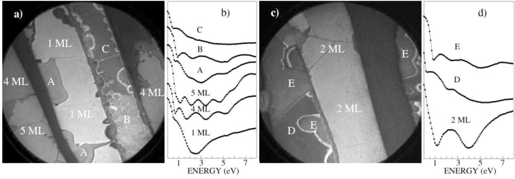
Two LEEM images from different locations of a graphene sample grown by high temperature sublimation are shown in
Figure 1a,c. These images were collected at a field of view (FOV) of 25 μm and energies of 3.9 eV and 5.1 eV, respectively. Several different domains are clearly visible, and the number of graphene layers present can be determined from the electron reflectivity
versus electron kinetic energy,
i.e., the so-called I(V) curve. The curves extracted from the different domains are displayed in
Figure 1b,d. The curve obtained from the lightest grey areas in
Figure 1a shows one minimum, which means [
15] that these areas have a graphene layer thickness of 1 ML. Other domains give curves with four and five pronounced minima, showing a thickness of 4 ML and 5 ML of graphene in these areas. The light grey areas in
Figure 1c is seen to have a coverage of 2 ML of graphene, since the corresponding I(V) curve in
Figure 1d exhibits two pronounced minima. The other curves, labeled A, B and C in
Figure 1b and D and E in
Figure 1d, do not show similarly well-defined and pronounced modulations of the reflectivity and, therefore, indicate areas where a mixture of different number of graphene layers exist. The really dark areas in both
Figure 1a,c showed no grapheme coverage, but presence of an ordered silicate, observed and discussed earlier [
7,
8,
9,
16,
17]. The essential point here was that large enough areas of 1 ML, 2 ML and 4 ML of graphene were identified by LEEM, so selected area PES, LEED and ARPES could be applied.
Figure 1.
Low Energy Electron Microscopy (LEEM) images collected at a field of view (FOV) of 25 μm from a C-face sample using an energy of (a) 3.9 eV and from another position (c) at an energy of 5.1 eV. The electron reflectivity curves in (b) and (d), extracted from different locations in (a) and (c), reveal fairly large areas of 1, 4 and 5 MLs and of 2 MLs of graphene, respectively.
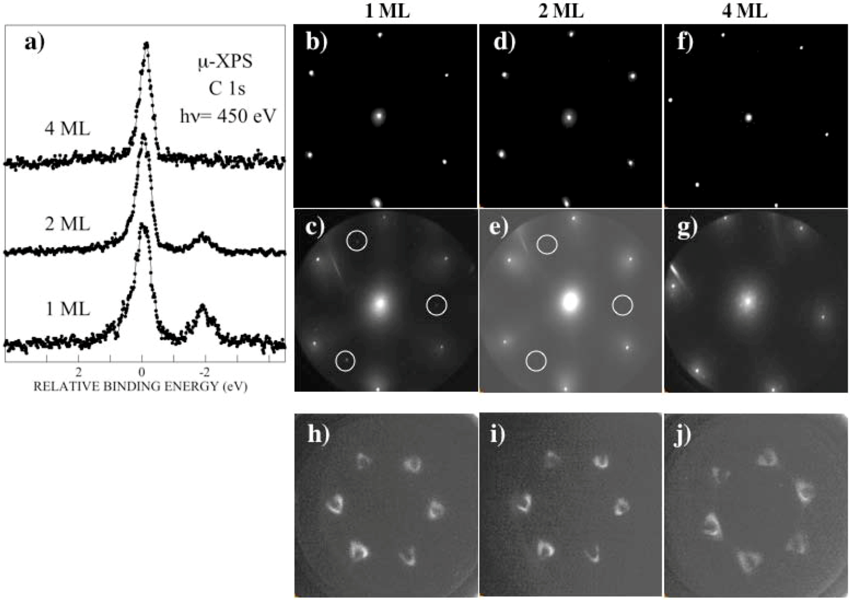
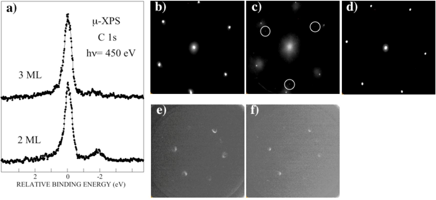
C 1s spectra collected using a photon energy of 450 eV and a probing area of 4 μm are displayed in
Figure 2a. A C 1s signal from the SiC substrate is clearly resolved, around 1.9 eV lower binding energy [
4,
9] than the graphene component, in the spectra from both the 1 ML and 2 ML areas. This peak is not discernible from areas having a 4 ML graphene coverage, which agrees well with earlier findings [
4,
9]. These C 1s spectra show no hint of a dense disordered carbon interface layer, which earlier has been proposed to be present, at least locally [
7,
16,
18]. Selected area LEED patterns collected using two different electron energies from the three areas with different graphene coverage are shown in
Figure 2b–g. A probing area of 1.5 μm is utilized, so the pattern is in each case collected from a single crystallographic grain having a specific number of graphene layers. The patterns collected at 45 eV (see
Figure 2b,d,f) all show a distinct (1 × 1) pattern and no presence of additional superstructure spots. When increasing the energy to 145 eV, additional weaker spots, of which three are marked by white circles, are possible to observe in the patterns from the 1 ML and 2 ML areas, while such spots are not visible in the pattern from the 4 ML area.
These weaker spots are located closer to the (0,0) spot than the graphene (1 × 1) spots, which indicate a different lattice constant. They are interpreted to originate from the SiC substrate, since the (1 × 1) diffraction spots from the SiC substrate and graphene appear at the same distances, within the experimental uncertainty, from the (0,0) spot for graphene grown on Si-face SiC [
4]. There, the substrate spots are always rotated 30° relative to the graphene (1 × 1) spots, and although the angle is close to 30°, also in this case, we observed at other locations and for other samples a different angle. Why three of the six diffraction spots from the substrate appear weaker than the other three, we have no clear explanation for, but a similar observation concerning relative intensities has earlier been reported for the (6√3 × 6√3)-R 30° buffer layer spots for Si-face graphene [
19]. That no diffraction spots related to the SiC substrate can be observed from the 4 ML area is expected, since this is also the case for graphene grown on Si-face SiC. No additional superstructure spots originating from graphene are thus observed in any of the μ-LEED patterns in
Figure 2. This clearly indicates that adjacent graphene layers in the 2 ML and 4 ML areas investigated are not rotationally disordered. To further demonstrate that the layers of graphene are stacked in such a way that no rotational disorder exists between adjacent layers, recorded constant energy photoelectron angular distribution patterns E
i(k
x,k
y) of the π-band from areas with a different number of graphene layers are shown in
Figure 2h–j. These patterns were collected using a probing area of 800 nm, a photon energy of 45 eV and at an energy of about 1.5 eV below the Fermi energy. Only the six Dirac cones, which appear triangular at this initial energy [
9], centered around the six K-points in the Brillouin zone are observed in these patterns. They thus show clearly that well-ordered grains of multilayer graphene larger than 800 nm have formed and that adjacent graphene layers are not rotated relative to each other.
Figure 2.
(
a) C 1s spectra collected, using a probing area of 4 μm, from domains in
Figure 1 with different graphene thickness; (
b)–(
g) show 1.5 μm selected area LEED patterns from; (
b) and (
c), the 1 ML domain at 45 and 145 eV; (
d) and (
e), the 2 ML domain at 45 and 145 eV; and (
f) and (
g), the 4 ML domain at 45 and 130 eV, respectively. In (
h)–(
j), the photoelectron angular distribution pattern (PAD) collected from, respectively, the 1 ML, 2 ML and 4 ML domains are shown. The PADs were collected at an energy of 1.5 eV below the Fermi level, using a probing area of 800 nm.
2.2. Samples Prepared by Sublimation at Lower Temperatures in High Vacuum
Other research groups have so far utilized growth temperatures considerably lower than 1900 °C when growing graphene on C-face SiC [
1,
2,
3,
4,
5,
7,
8,
10,
16,
17,
20]. They have moreover reported [
7,
8,
16,
17,
20] formation of smaller domains and grain sizes considerably smaller than 2 μm, so selected area LEED patterns collected looked practically identical to large-area LEED patterns. Only when prepared under a high pressure of disilane,
i.e., in the 10
−5 mbar range, larger grains were found to form, but the selected area LEED pattern obtained [
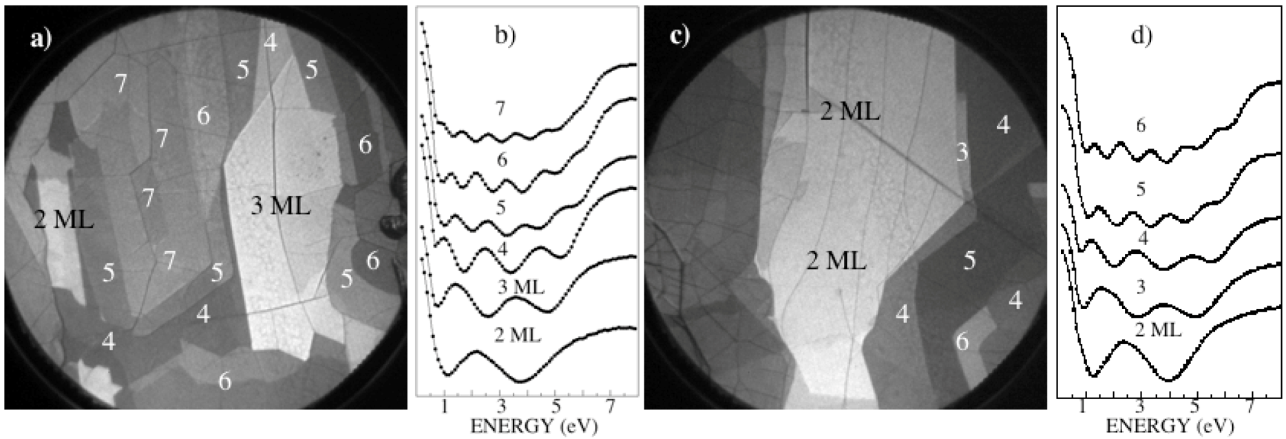
8] was very complex. Therefore, we also prepared graphene on C-face SiC using lower sublimation temperatures and in high vacuum conditions. The main purpose was to see if domains and grain sizes large enough that a single grain could be probed was possible to achieve using such a growth procedure. If such large grains of multilayer graphene were obtained, another purpose was to investigate if these grains would show rotational disorder between the layers or not. Temperatures of 1350, 1450 and 1500 °C were tried, and the best result was obtained at 1500 °C. At 1450 °C, the graphene domain and grain sizes achieved were significantly smaller than after growth at 1500 °C. Two LEEM images from different locations of a graphene sample grown by sublimation at a temperature of 1500 °C for 15 min and in high vacuum,
i.e., the 10
−5 mbar range, are shown in
Figure 3a,c. These images were collected at a FOV of 15 μm and energies of 1.8 eV and 2.0 eV, respectively. Several different domains are clearly visible, and the number of graphene layers present is revealed by the number of minima in the extracted I(V) curves displayed in
Figure 3b,d, respectively. The number of layers varies from 2 to 7 in these images, so the formation of graphene is fairly non uniform. However, the bright grey areas show that one large domain with 3 MLs of graphene, in
Figure 3a, and one with 2 MLs of graphene, in
Figure 3c, have formed on this sample.
Figure 3.
LEEM images collected at a field of view (FOV) of 15 μm from an in situ C-face sample using an energy of (a) 1.8 eV and from another position (c) at an energy of 2.0 eV. The electron reflectivity curves in (b) and (d) extracted from different locations in (a) and (c) reveal fairly large areas of 3 MLs and 2 MLs of graphene, respectively.
The C 1s spectra collected from these two areas using a photon energy of 450 eV and a probing area of 4 μm are displayed in
Figure 4a. The C 1s signal from the SiC substrate is clearly observed in the spectrum from the 2 ML area, while it is barely visible in the spectrum from the 3 ML area. No hint of a dense disordered carbon interface layer [
7,
16,
19] is discernible either in these C 1s spectra. Selected area LEED patterns collected from the 2 ML and 3 ML areas are shown in
Figure 4b–d. A probing area of 1.5 μm was utilized, so each pattern is again collected from a single crystallographic grain having a specific number of graphene layers. The patterns collected at 45 eV (see
Figure 4b,d), both show distinct (1 × 1) patterns and no additional superstructure spots. When increasing the energy to 200 eV, three additional weaker spots appear in the pattern from the 2 ML area (see
Figure 4c). These appear at the same distance from the (0,0) spot as the weak ones observed in
Figure 2c,e and are therefore also interpreted to originate from the underlying SiC substrate. To note here is that the angle of rotation between the (1 × 1) diffraction spots from the graphene and the SiC substrate is very different compared to that obtained in
Figure 2, which was close to the 30° always observed between the graphene and the SiC substrate spots in LEED patterns from the Si-terminated surface. There, the carbon buffer layer acts as a template and fixes the angle to 30°, while on the C-face, no such buffer layer forms and islands of graphene can nucleate at different rotation angles relative to the SiC substrate [
4,
7,
8,
16,
17]. The important point that we want to stress here is, however, that no superstructure spots are observed in these μ-LEED patterns and that this shows that there is no rotational disorder between adjacent layers on the 2 MLs and 3 MLs areas of this sample prepared by sublimation at 1500 °C in high vacuum. To further emphasize this point, constant energy photoelectron angular distribution patterns E
i(k
x,k
y) of the π-band recorded from the 2 ML area are shown in
Figure 4e,f. These patterns were collected using a probing area of 800 nm, a photon energy of 45 eV and at energies of about 1.0 eV and 0.5 eV, respectively, below the Fermi energy. Only the six Dirac cones centered around the six K-points in the Brillouin zone are observed in these patterns. Two of the cones are very weak in these patterns. This is probably due to symmetry selection rules related to the experimental geometry, since this was also visible in the patterns displayed in
Figure 2h–j, and also, there, this effect became more pronounced at energies closer to the Fermi energy. Anyhow, the patterns in
Figure 4e,f show clearly that well-ordered grains of multilayer graphene larger than 800 nm have formed on this sample and that adjacent graphene layers are not rotated relative to each other. The same results were obtained from samples of a few layers of graphene grown at 1450 °C for 15 min and at 1500 °C for 10 min, although the domain and grain sizes were in general found to be somewhat smaller than for the above described sample.
Figure 4.
(
a) C 1s spectra collected, using a probing area of 4 μm, from domains in
Figure 3 with different graphene thickness; (
b)–(
d) show 1.5 μm selected area LEED patterns from: (
b) and (
c), the 2 ML domain at 45 and 200 eV; (
d), the 3 ML domain at 45 eV, respectively; in (
e)–(
f), PADs collected from the 2 ML domain in
Figure 3c, using a probing area of 800 nm, and at energies of 1.0 and 0.5 eV below the Fermi level are shown.
2.3. Samples Treated in Hydrogen
A LEEM image, collected at 1.7 eV and a FOV of 50 μm, from a sample grown at 1900 °C for 15 min in an argon pressure of 850 mbar, is shown in
Figure 5a. It is a representative image of the surface morphology, since similar images were obtained at other positions on this sample. After hydrogen treatment, the LEEM images obtained were distinctly different, as illustrated by the representative image in
Figure 5b. The domain structure clearly observed on the as-grown sample has more or less disappeared after hydrogen treatment, and considerably smaller domains and contrast variations are observed. For the as-grown sample, in
Figure 5a, I(V) curves showing pronounced periodic variations indicating a coverage of mainly 3 and 4 MLs of graphene could be extracted. For the hydrogen treated sample,
Figure 5b, extracted I(V) curves also showed periodic variations, but considerably less pronounced. Selected area LEED patterns collected appeared clear and distinct, but were found to change with time when using the typical μ-LEED electron beam current of 200 nA. The beam actually produced changes on the surface that were clearly detectable by LEEM after only a few minutes exposure, as illustrated in
Figure 5c,d. This hydrogen treated sample was grown under the same conditions as the sample shown in
Figure 3,
i.e., by sublimation at a temperature of 1500 °C for 15 min and in high vacuum. It was deliberately exposed to the typical μ-LEED electron beam current over an area with radius of
ca. 5 μm for about two minutes. The illuminated circular area appears darker and brighter in the LEEM images in
Figure 5c,d that were collected at a FOV of 25 μm and energies of 1.7 eV and 6.5 eV, respectively. This clearly demonstrates that the typical μ-LEED electron beam current does induce changes in hydrogen treated C-face graphene samples, and hydrogen desorption appears the most likely reason. Before looking at how the μ-LEED pattern typically changed with time, it deserves to be mentioned that for this hydrogenated sample, in
Figure 5c,d, the I(V) curves extracted outside the illuminated circular area did not show any periodic oscillations, but instead appeared similar to curve C in
Figure 1b, irrespective of the size and position of the area selected. For this sample, the hydrogen treatment thus drastically affected the size of the domains and apparently also perturbed the periodicity in distance between the graphene sheets, since no interference effect was possible to observe in extracted reflectivity curves.
Figure 5.
LEEM image collected at 1.7 eV and a FOV of 50 μm, from a C-face sample (a) as-grown and (b) after hydrogen treatment. The images in (c) and (d) were collected at a FOV of 25 μm from another hydrogen treated sample at an energy of 1.7 eV and 6.5 eV, respectively. The circular dark and bright spot observed in (c) and (d) was created by electron beam illumination during collection of μ-LEED images.
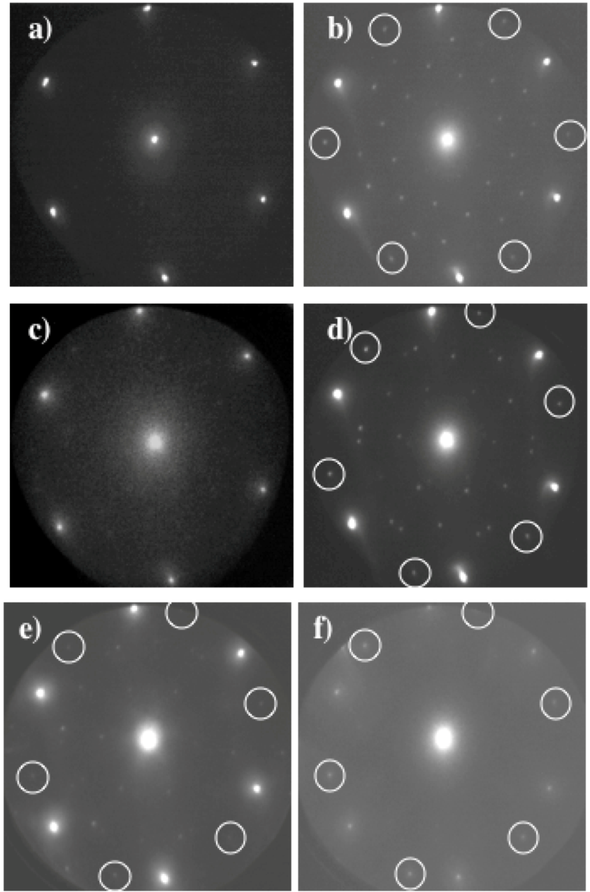
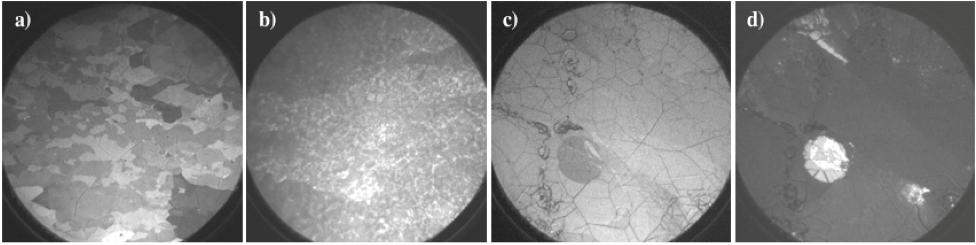
The μ-LEED pattern in
Figure 6b was recorded two minutes after that in 6a from the same spot of the hydrogen treated sample. An energy 45 eV and a probing area of 1.5 μm was selected, and this sample was the one initially prepared at 1500 °C in high vacuum. The superstructure spots become clearly visible after only about one minute of electron beam exposure. The strongest of the superstructure spots are marked by white circles in
Figure 6b, and they are seen to have the same distance to the (0,0) spot as the initial (1 × 1) graphene spots. In addition to these strong spots, there are other spots arranged in inner hexagonal patterns, like in the patterns recently reported [
21] for specially prepared twisted bilayer graphene samples. When decreasing the μ-LEED electron beam current, to 10 nA, and moving to another spot on the sample, the pattern in
Figure 6c was obtained, which again is mainly a (1 × 1) graphene pattern. When increasing the electron beam current again, to 200 nA, the pattern in
Figure 6d resulted, which shows a similar set of six strong superstructure spots, although now at a different rotation angle. When increasing the electron energy to 80 eV and 142 eV, the same pattern remained (see
Figure 6e,f), only the relative intensity between the main and superstructure spots are changed. These superstructure spots can be explained in the same way as earlier proposed [
21] for twisted bilayer graphene samples, indicating a twist angle of around 35° and 20° in
Figure 6b,d, respectively. Since this effect with electron beam exposure did not occur for the as-prepared graphene C-face samples, hydrogen desorption appears as the most plausible explanation. Moreover, after local hydrogen desorption by electron beam illumination, the two uppermost graphene layers appear in general to be twisted relative to each other, which definitely was not the case on the large ordered grains on the as-prepared samples (see
Figure 2 and
Figure 4). Therefore, the hydrogen treated sample was also heated
in situ at 600 °C for a couple of minutes in an effort to desorb most of the hydrogen.
Figure 6.
(a) to (d), LEED patterns from a hydrogenated sample at an energy of 45 eV and a probing area of 1.5 μm. The pattern was found to change from the (1 × 1) in (a) to that in (b), containing superstructure spots within a minute. When moving to another spot on the sample and using a low electron beam current, the 1 × 1 pattern in (c) was observed. When increasing to the high electron beam current, the pattern in d) appeared within a minute. Using electron energies of 80 eV and 142 eV resulted in the patterns shown in (e) and (f), respectively.
The μ-LEED patterns collected afterwards using the normal typical high electron current then showed no time effect. Stable (1 × 1) patterns, but also patterns containing superstructure spots similar to those in
Figure 6, were then obtained at different positions on the surface. However, extracted I(V) curves still did not show pronounced periodic variations; they still appeared similar to curve C in
Figure 1b, irrespective of the size and position of the area selected. Before heating, μ-PES core level spectra were collected from the hydrogen treated samples, both from areas previously illuminated and not illuminated by the LEED electron beam. No difference in the chemical composition between these areas could be revealed by the core level spectra, which suggests local hydrogen desorption as the probable origin to the changes observed in the LEEM images in
Figure 5c,d. A hydrogen treatment, which for Si-face graphene results in intercalation and improved properties, for C-face graphene instead result in deteriorated properties. The average grain/domain size is drastically reduced; adjacent graphene layers appeared for one sample to become decoupled, since no clear interference effect was observable in extracted I(V) curves, and after local hydrogen desorption by the electron beam, adjacent graphene layers are in general rotated relative to each other. Heat treatment of a hydrogenated C-face graphene sample did neither restore the quality of the original as-grown sample; considerably smaller domain/grain sizes showing either (1 × 1) or twisted layer μ-LEED patterns were then observed. Thus, the hydrogen treatment tried for the C-face graphene samples had, contrary to the case for Si-face graphene, a detrimental effect on the quality and properties of the graphene.
