
Effects of Substrate Polarity and Pre-Growth Treatments on Plasma-Assisted Molecular-Beam Epitaxy of β-Ga2O3 on 4° Off-Axis 4H-SiC

 , , , and
Abstract
1. Introduction
2. Experimental Details
- I.
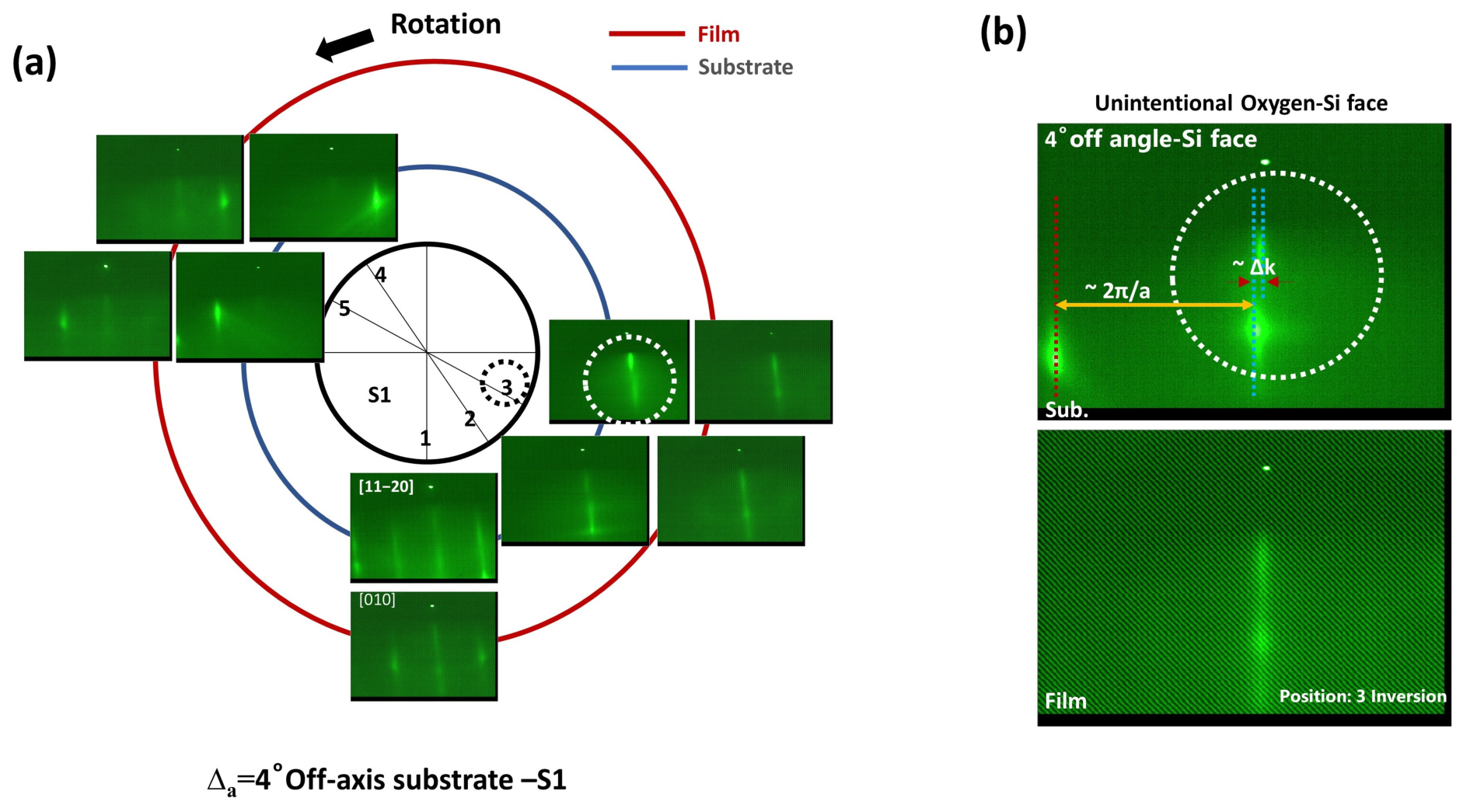
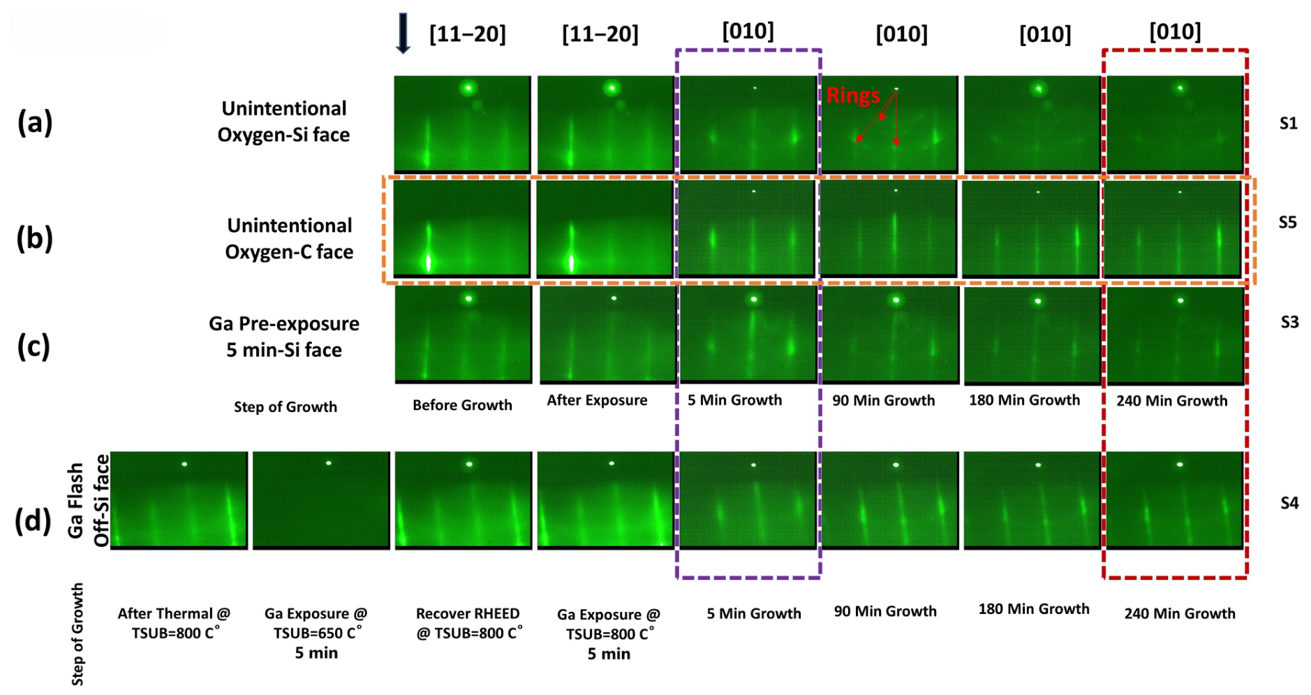
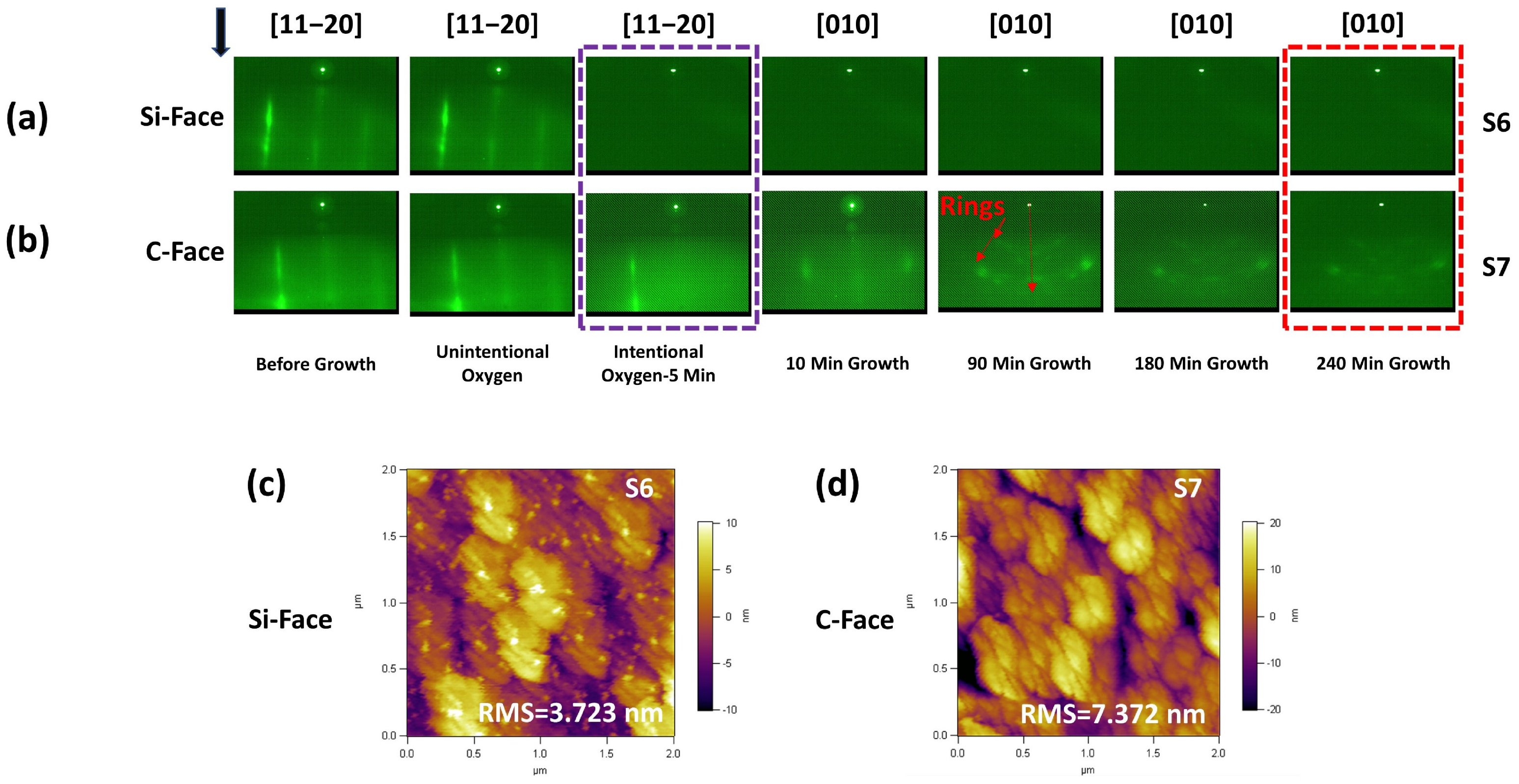
- Unintentional oxygen exposure: By supplying the oxygen gas to turn on the oxygen-plasma cell, the substrate is naturally exposed to the oxygen gas. Just after supplying the oxygen gas, RF oxygen plasma was turned on with an RF power of 300 W and an oxygen flow rate of 2 SCCM, while both the plasma shutter for the plasma cell and the main shutter for the substrate were closed. Then, both oxygen and Ga shutters were opened simultaneously followed by the opening of the main shutter for the growth of β-Ga2O3 films. Recording the RHEED patterns was assessed when plasma was turned on, while both the plasma shutter and main shutter were closed.
- II.
- Intentional Ga pre-exposure: Ga beam (TGa cell = 820 °C) pre-exposure treatment was intentionally performed. The thermally cleaned substrate was initially subjected to Ga flux (TGa cell = 820 °C) for a short time [two samples were grown: S2 with Ga exposure for 1 min and S3 with Ga exposure for 5 min]. The oxygen plasma was then stabilized while Ga was continuously supplied to the substrate. After plasma stabilization, the oxygen plasma shutter was opened to start β-Ga2O3 growth, while the main shutter had already been opened for Ga exposure.
- III.
- Ga flash-off, followed by Ga pre-exposure: In this process, to mitigate possible residual oxide-related surface effects on the Si-face 4H-SiC substrate, the thermally cleaned substrate was exposed to Ga flux at a low substrate temperature of 650 °C (Tsubstrate = 650 °C). After this step, the Ga pre-exposure procedures in II were carried out.
- IV.
- Intentional oxygen-plasma pre-exposure: In this process, when the oxygen-plasma was stabilized, the oxygen shutter and the main shutter were opened and substrates were exposed to energetic oxygen for 5 min, while the Ga shutter was closed. Then, the Ga shutter was opened to start the growth of the film.
3. Results and Discussion
3.1. In Situ RHEED Characterization of Atomic Steps on 4° Off-Axis 4H-SiC Substrate
3.2. Effects of Pre-Growth Treatments on the Morphology of Ga2O3 Films Grown on 4° Off-Axis Surfaces
3.2.1. Growth on On-Axis and 4° Off-Axis Substrates
3.2.2. Growth Evaluation by In Situ RHEED Observations
3.2.3. Morphological Characteristics
3.2.4. Intentional Oxygen-Plasma Pre-Exposure
3.3. Structural Investigations by XRD
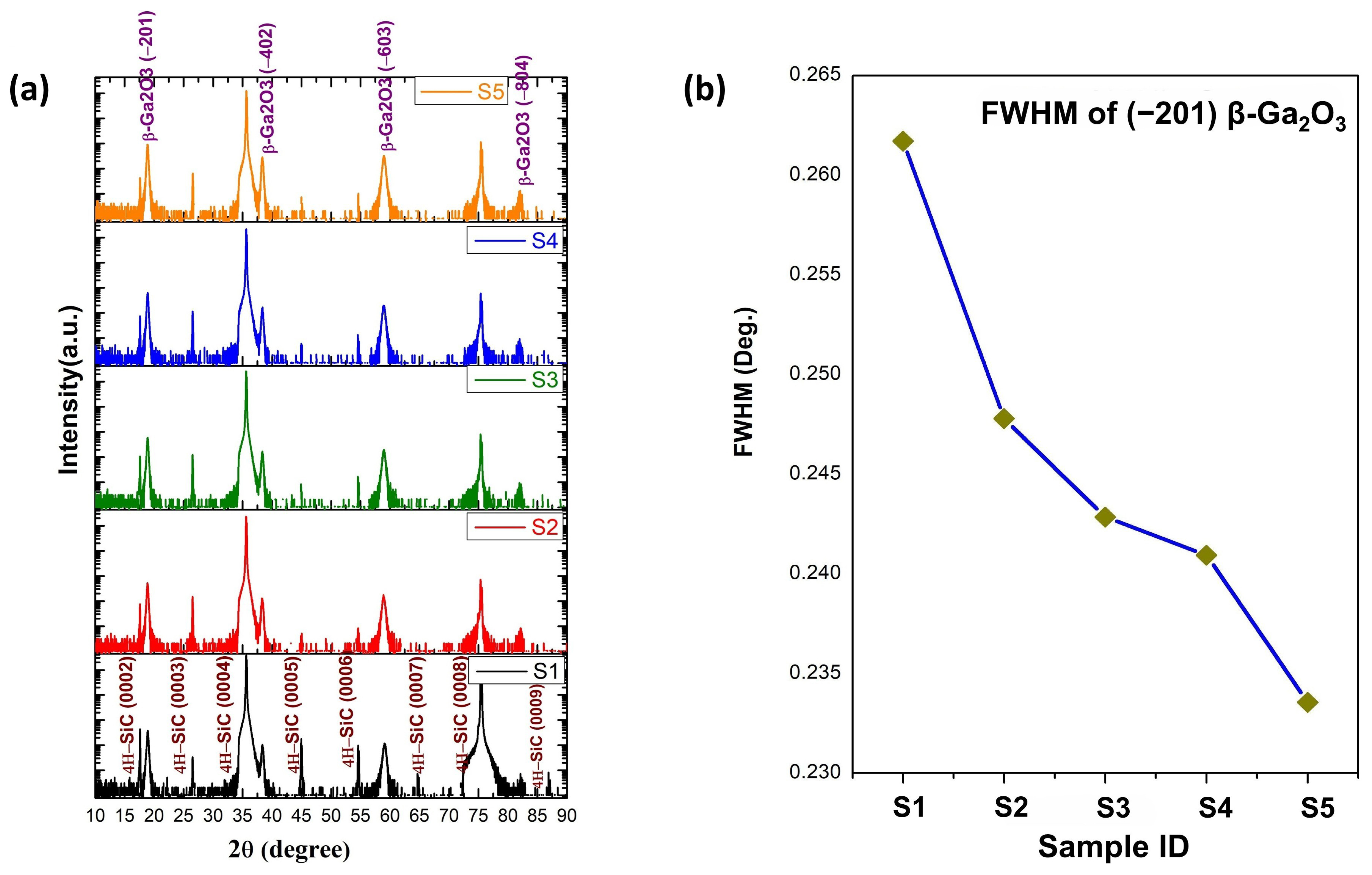
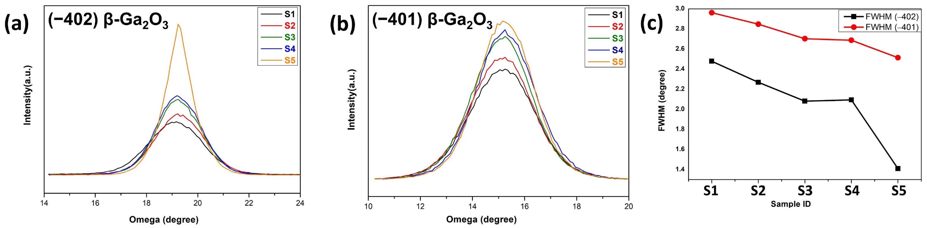
3.3.1. Crystallographic Orientation of the β-Ga2O3 Films and Crystal Quality
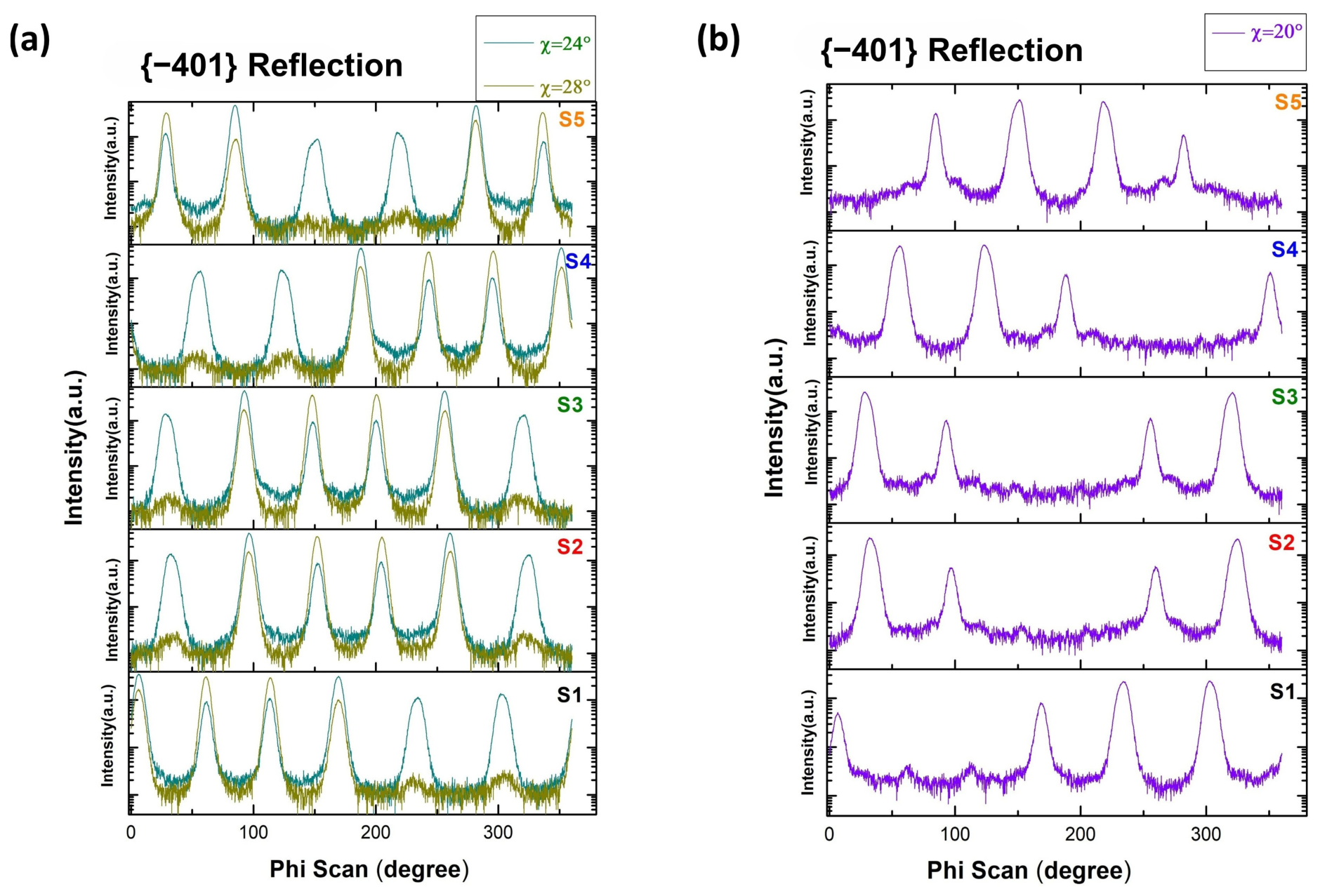
3.3.2. Rotational-Domain-Related φ-Scan Features in β-Ga2O3 Films
4. Summary
Author Contributions
Funding
Data Availability Statement
Conflicts of Interest
Correction Statement
Abbreviations
| PAMBE | Plasma-assisted molecular-beam epitaxy |
| RHEED | Reflection high-energy electron diffraction |
| AFM | Atomic force microscope |
| HRXRD | High-resolution X-ray diffraction |
| Ω-XRC | Ω-x-ray rocking curve |
References
- Pearton, S.J.; Yang, J.; Cary, P.H.; Ren, F.; Kim, J.; Tadjer, M.J.; Mastro, M.A. A Review of Ga2O3 Materials, Processing, and Devices. Appl. Phys. Rev. 2018, 5, 011301. [Google Scholar] [CrossRef] [Scilit]
- Tsao, J.Y.; Chowdhury, S.; Hollis, M.A.; Jena, D.; Johnson, N.M.; Jones, K.A.; Simmons, J.A.; Kaplar, R.J.; Rajan, S.; Van de Walle, C.G.; et al. Ultrawide-bandgap Semiconductors: Research Opportunities and Challenges. Adv. Electron. Mater. 2018, 4, 1600501. [Google Scholar] [CrossRef] [Scilit]
- Pearton, S.J.; Ren, F.; Tadjer, M.; Kim, J. Perspective: Ga2O3 for Ultra-high Power Rectifiers and MOSFETS. J. Appl. Phys. 2018, 124, 220901. [Google Scholar] [CrossRef] [Scilit]
- Roy, R.; Hill, V.G.; Osborn, E.F. Polymorphism of Ga2O3 and the System Ga2O3–H2O. J. Am. Chem. Soc. 1952, 74, 719–722. [Google Scholar] [CrossRef] [Scilit]
- Hoshikawa, K.; Ohba, E.; Kobayashi, T.; Yanagisawa, J.; Miyagawa, C.; Nakamura, Y. Growth of β-Ga2O3 Single Crystals Using Vertical Bridgman Method in Ambient Air. J. Cryst. Growth 2016, 447, 36–41. [Google Scholar] [CrossRef] [Scilit]
- Tomm, Y.; Reiche, P.; Klimm, D.; Fukuda, T. Czochralski Grown Ga2O3 Crystals. J. Cryst. Growth 2000, 220, 510–514. [Google Scholar] [CrossRef] [Scilit]
- Aida, H.; Nishiguchi, K.; Takeda, H.; Aota, N.; Sunakawa, K.; Yaguchi, Y. Growth of β-Ga2O3 Single Crystals by the Edge-Defined, Film Fed Growth Method. Jpn. J. Appl. Phys. 2008, 47, 8506. [Google Scholar] [CrossRef] [Scilit]
- Galazka, Z.; Uecker, R.; Irmscher, K.; Albrecht, M.; Klimm, D.; Pietsch, M.; Brützam, M.; Bertram, R.; Ganschow, S.; Fornari, R. Czochralski Growth and Characterization of β-Ga2O3 Single Crystals. Cryst. Res. Technol. 2010, 45, 1229–1236. [Google Scholar] [CrossRef] [Scilit]
- Rafique, S.; Han, L.; Neal, A.T.; Mou, S.; Tadjer, M.J.; French, R.H.; Zhao, H. Heteroepitaxy of N-Type β-Ga2O3 Thin Films on Sapphire Substrate by Low Pressure Chemical Vapor Deposition. Appl. Phys. Lett. 2016, 109, 132103. [Google Scholar] [CrossRef] [Scilit]
- Orita, M.; Ohta, H.; Hirano, M.; Hosono, H. Deep-Ultraviolet Transparent Conductive β-Ga2O3 Thin Films. Appl. Phys. Lett. 2000, 77, 4166–4168. [Google Scholar] [CrossRef] [Scilit]
- Víllora, E.G.; Shimamura, K.; Yoshikawa, Y.; Ujiie, T.; Aoki, K. Electrical Conductivity and Carrier Concentration Control in β-Ga2O3 by Si Doping. Appl. Phys. Lett. 2008, 92, 202120. [Google Scholar] [CrossRef] [Scilit]
- Pearton, S.J.; Ren, F.; Polyakov, A.Y.; Yakimov, E.B.; Chernyak, L.; Haque, A. Perspective on Comparative Radiation Hardness of Ga2O3 Polymorphs. J. Vac. Sci. Technol. A 2025, 43, 038501. [Google Scholar] [CrossRef] [Scilit]
- Yang, J.; Ren, F.; Pearton, S.J.; Yang, G.; Kim, J.; Kuramata, A. 1.5 MeV Electron Irradiation Damage in β-Ga2O3 Vertical Rectifiers. J. Vac. Sci. Technol. B 2017, 35, 031208. [Google Scholar] [CrossRef] [Scilit]
- Szalkai, D.; Galazka, Z.; Irmscher, K.; Tutto, P.; Klix, A.; Gehre, D. β-Ga2O3 Solid-State Devices for Fast Neutron Detection. IEEE Trans. Nucl. Sci. 2017, 64, 1574–1579. [Google Scholar] [CrossRef] [Scilit]
- Battiston, G.A.; Gerbasi, R.; Porchia, M.; Bertoncello, R.; Caccavale, F. Chemical Vapour Deposition and Characterization of Gallium Oxide Thin Films. Thin Solid Films 1996, 279, 115–118. [Google Scholar] [CrossRef] [Scilit]
- Wagner, G.; Baldini, M.; Gogova, D.; Schmidbauer, M.; Schewski, R.; Albrecht, M.; Galazka, Z.; Klimm, D.; Fornari, R. Homoepitaxial Growth of β-Ga2O3 Layers by Metal-Organic Vapor Phase Epitaxy. Phys. Status Solidi A 2014, 211, 27–33. [Google Scholar] [CrossRef] [Scilit]
- Orita, M.; Hiramatsu, H.; Ohta, H.; Hirano, M.; Hosono, H. Preparation of Highly Conductive, Deep Ultraviolet Transparent β-Ga2O3 Thin Film at Low Deposition Temperatures. Thin Solid Films 2002, 411, 134–139. [Google Scholar] [CrossRef] [Scilit]
- Nomura, K.; Goto, K.; Togashi, R.; Murakami, H.; Kumagai, Y.; Kuramata, A.; Yamakoshi, S.; Koukitu, A. Thermodynamic Study of β-Ga2O3 Growth by Halide Vapor Phase Epitaxy. J. Cryst. Growth 2014, 405, 19–22. [Google Scholar] [CrossRef] [Scilit]
- Fleischer, M.; Hanrieder, W.; Meixner, H. Stability of Semiconducting Gallium Oxide Thin Films. Thin Solid Films 1990, 190, 93–102. [Google Scholar] [CrossRef] [Scilit]
- Ogita, M.; Yuasa, S.; Kobayashi, K.; Yamada, Y.; Nakanishi, Y.; Hatanaka, Y. Presumption and Improvement for Gallium Oxide Thin Film of High Temperature Oxygen Sensors. Appl. Surf. Sci. 2003, 212–213, 397–401. [Google Scholar] [CrossRef] [Scilit]
- Shan, F.K.; Liu, G.X.; Lee, W.J.; Lee, G.H.; Kim, I.S.; Shin, B.C. Structural, Electrical, and Optical Properties of Transparent Gallium Oxide Thin Films Grown by Plasma-Enhanced Atomic Layer Deposition. J. Appl. Phys. 2005, 98, 023504. [Google Scholar] [CrossRef] [Scilit]
- Wu, C.; Guo, D.Y.; Zhang, L.Y.; Li, P.G.; Zhang, F.B.; Tan, C.K.; Wang, S.L.; Liu, A.P.; Wu, F.M.; Tang, W.H. Systematic Investigation of the Growth Kinetics of β-Ga2O3 Epilayer by Plasma Enhanced Chemical Vapor Deposition. Appl. Phys. Lett. 2020, 116, 072102. [Google Scholar] [CrossRef] [Scilit]
- Oshima, T.; Okuno, T.; Fujita, S. Ga2O3 Thin Film Growth on C-Plane Sapphire Substrates by Molecular Beam Epitaxy for Deep-Ultraviolet Photodetectors. Jpn. J. Appl. Phys. 2007, 46, 7217. [Google Scholar] [CrossRef] [Scilit]
- Tsai, M.Y.; Bierwagen, O.; White, M.E.; Speck, J.S. β-Ga2O3 Growth by Plasma-Assisted Molecular Beam Epitaxy. J. Vac. Sci. Technol. A 2010, 28, 354–359. [Google Scholar] [CrossRef] [Scilit]
- Oshima, T.; Arai, N.; Suzuki, N.; Ohira, S.; Fujita, S. Surface Morphology of Homoepitaxial β-Ga2O3 Thin Films Grown by Molecular Beam Epitaxy. Thin Solid Films 2008, 516, 5768–5771. [Google Scholar] [CrossRef] [Scilit]
- Víllora, E.G.; Shimamura, K.; Kitamura, K.; Aoki, K. Rf-Plasma-Assisted Molecular-Beam Epitaxy of β-Ga2O3. Appl. Phys. Lett. 2006, 88, 031105. [Google Scholar] [CrossRef] [Scilit]
- Santia, M.D.; Tandon, N.; Albrecht, J.D. Lattice Thermal Conductivity in β-Ga2O3 from First Principles. Appl. Phys. Lett. 2015, 107, 041907. [Google Scholar] [CrossRef] [Scilit]
- Oh, J.; Ma, J.; Yoo, G. Simulation Study of Reduced Self-Heating in β-Ga2O3 MOSFET on a Nano-Crystalline Diamond Substrate. Results Phys. 2019, 13, 102151. [Google Scholar] [CrossRef] [Scilit]
- Nepal, N.; Katzer, D.S.; Downey, B.P.; Wheeler, V.D.; Nyakiti, L.O.; Storm, D.F.; Meyer, D.J.; Hardy, M.T.; Freitas, J.A.; Jin, E.N.; et al. Heteroepitaxial Growth of β-Ga2O3 Films on SiC via Molecular Beam Epitaxy. J. Vac. Sci. Technol. A 2020, 38, 063406. [Google Scholar] [CrossRef] [Scilit]
- Cheng, Z.; Mu, F.; You, T.; Xu, W.; Shi, J.; Liao, M.E.; Graham, S.; Wang, Y.; Huynh, K.; Suga, T.; et al. Thermal Transport across Ion-Cut Monocrystalline β-Ga2O3 Thin Films and Bonded β-Ga2O3–SiC Interfaces. ACS Appl. Mater. Interfaces 2020, 12, 44943–44951. [Google Scholar] [CrossRef] [Scilit] [PubMed]
- Zhu, N.; Ma, K.; Xue, X.; Su, J. The Formation and Role of the SiO2 Oxidation Layer in the 4H-SiC/β-Ga2O3 Interface. Appl. Surf. Sci. 2022, 581, 151956. [Google Scholar] [CrossRef] [Scilit]
- Xu, B.; Hu, J.; Meng, J.; He, X.; Wang, X.; Pu, H. Study of the Bonding Characteristics at β-Ga2O3 (01)/4H-SiC (0001) Interfaces from First Principles and Experiment. Crystals 2023, 13, 160. [Google Scholar] [CrossRef] [Scilit]
- Brown, A.S.; Losurdo, M.; Kim, T.H.; Giangregorio, M.M.; Choi, S.; Morse, M.; Wu, P.; Capezzuto, P.; Bruno, G. The Impact of SiC Substrate Treatment on the Heteroepitaxial Growth of GaN by Plasma-Assisted MBE. Cryst. Res. Technol. 2005, 40, 997–1002. [Google Scholar] [CrossRef] [Scilit]
- Hong, S.K.; Ko, H.J.; Chen, Y.; Hanada, T.; Yao, T. Control and Characterization of ZnO/GaN Heterointerfaces in Plasma-Assisted MBE-Grown ZnO Films on GaN/Al2O3. Appl. Surf. Sci. 2000, 159, 441–448. [Google Scholar] [CrossRef] [Scilit]
- Hu, J.; Yang, X.; Meng, J.; Li, Y.; Xu, B.; Zhang, Q.; Yuan, L.; He, X. Effects of Off-Axis Angles of 4H-SiC Substrates on Properties of β-Ga2O3 Films Grown by Low-Pressure Chemical Vapor Deposition. Appl. Surf. Sci. 2025, 680, 161377. [Google Scholar] [CrossRef] [Scilit]
- Jantawongrit, P.; Sanorpim, S.; Yaguchi, H.; Orihara, M.; Limsuwan, P. Influence of Off-Cut Angle of (0001) 4H-SiC on the Crystal Quality of InN Grown by RF-MBE. Procedia Eng. 2012, 32, 882–887. [Google Scholar] [CrossRef] [Scilit]
- Hu, J.; Xu, B.; Zhang, Z.; He, X.; Li, L.; Cheng, H.; Pu, H.; Wang, J.; Meng, J.; Wang, X.; et al. Step Flow Growth of β-Ga2O3 Films on Off-Axis 4H-SiC Substrates by LPCVD. Surf. Interfaces 2023, 37, 102732. [Google Scholar] [CrossRef] [Scilit]
- Schewski, R.; Lion, K.; Fiedler, A.; Wouters, C.; Popp, A.; Levchenko, S.V.; Schulz, T.; Schmidbauer, M.; Bin Anooz, S.; Grüneberg, R.; et al. Step-Flow Growth in Homoepitaxy of β-Ga2O3 (100)—The Influence of the Miscut Direction and Faceting. APL Mater. 2019, 7, 022515. [Google Scholar]
- Oshima, T. Step-and-Terrace Surface Formation on (001) β-Ga2O3 by Wet Etching Using 2.38 Wt% Tetramethylammonium Hydroxide (TMAH) Lithographic Developer. Jpn. J. Appl. Phys. 2025, 64, 088001. [Google Scholar] [CrossRef] [Scilit]
- Yoshimoto, M.; Maeda, T.; Ohnishi, T.; Koinuma, H.; Ishiyama, O.; Shinohara, M.; Kubo, M.; Miyamoto, A. Atomic-Scale Formation of Ultrasmooth Surfaces on Sapphire Substrates for High-Quality Thin-Film Fabrication. Appl. Phys. Lett. 1995, 67, 2615–2617. [Google Scholar] [CrossRef] [Scilit]
- Sasaki, K.; Higashiwaki, M.; Kuramata, A.; Masui, T.; Yamakoshi, S. Growth Temperature Dependences of Structural and Electrical Properties of Ga2O3 Epitaxial Films Grown on β-Ga2O3 (010) Substrates by Molecular Beam Epitaxy. J. Cryst. Growth 2014, 392, 30–33. [Google Scholar] [CrossRef] [Scilit]
- Mazzolini, P.; Falkenstein, A.; Wouters, C.; Schewski, R.; Markurt, T.; Galazka, Z.; Martin, M.; Albrecht, M.; Bierwagen, O. Substrate-Orientation Dependence of β-Ga2O3 (100), (010), (001), and (−201) Homoepitaxy by Indium-Mediated Metal-Exchange Catalyzed Molecular Beam Epitaxy (MEXCAT-MBE). APL Mater. 2020, 8, 011107. [Google Scholar] [CrossRef] [Scilit]
- Ngo, T.S.; Le, D.D.; Vuong, N.Q.; Hong, S.K. Systematic Investigation of Growth and Properties of Ga2O3 Films on c-Plane Sapphire Substrates Prepared by Plasma-Assisted Molecular Beam Epitaxy. ECS J. Solid State Sci. Technol. 2022, 11, 035008. [Google Scholar] [CrossRef] [Scilit]
- Cuccureddu, F.; Murphy, S.; Shvets, I.V.; Porcu, M.; Zandbergen, H.W.; Sidorov, N.S.; Bozhko, S.I. Surface Morphology of C-Plane Sapphire (α-Alumina) Produced by High Temperature Anneal. Surf. Sci. 2010, 604, 1294–1299. [Google Scholar] [CrossRef] [Scilit]
- Ilhom, S.; Mohammad, A.; Shukla, D.; Grasso, J.; Willis, B.G.; Okyay, A.K.; Biyikli, N. Low-Temperature As-Grown Crystalline β-Ga2O3 Films via Plasma-Enhanced Atomic Layer Deposition. ACS Appl. Mater. Interfaces 2021, 13, 8538–8551. [Google Scholar] [CrossRef] [Scilit] [PubMed]
- Gogova, D.; Tran, D.Q.; Stanishev, V.; Jokubavicius, V.; Vines, L.; Schubert, M.; Yakimova, R.; Paskov, P.P.; Darakchieva, V. High Crystalline Quality Homoepitaxial Si-doped β-Ga2O3 (010) Layers with Reduced Structural Anisotropy Grown by hot-wall MOCVD. J. Vac. Sci. Technol. A 2024, 42, 022708. [Google Scholar] [CrossRef] [Scilit]
- Qu, Y.; Wu, Z.; Ai, M.; Guo, D.; An, Y.; Yang, H.; Tang, W.; Li, L. Enhanced Ga2O3/SiC Ultraviolet Photodetector with Graphene Top Electrodes. J. Alloys Compd. 2016, 680, 247–251. [Google Scholar] [CrossRef] [Scilit]
- Toyoshima, H.; Shitara, T.; Zhang, J.; Neave, J.H.; Joyce, B.A. A Systematic RHEED Study of Regular and Random Steps on GaAs(001) Surfaces. Surf. Sci. 1992, 264, 10–22. [Google Scholar] [CrossRef] [Scilit]
- Larsen, P.K.; Dobson, P.J. (Eds.) Reflection High-Energy Electron Diffraction and Reflection Electron Imaging of Surfaces; NATO Science Series B; Springer Science & Business Media: New York, NY, USA, 2012; Volume 188. [Google Scholar]
- Crook, G.E.; Däweritz, L.; Ploog, K. In Situ Monitoring of Step Arrays on Vicinal silicon(100) Surfaces for Heteroepitaxy. Phys. Rev. B 1990, 42, 5126. [Google Scholar] [CrossRef] [Scilit]
- Chalmers, S.A.; Gossard, A.C.; Petroff, P.M.; Gaines, J.M.; Kroemer, H. A Reflection High-Energy Electron Diffraction Study of (100) GaAs Vicinal Surfaces. J. Vac. Sci. Technol. B 1989, 7, 1357–1362. [Google Scholar] [CrossRef] [Scilit]
- Feng, Z.; Karim, M.R.; Zhao, H. Low-Pressure Chemical Vapor Deposition of β-Ga2O3 Thin Films: Dependence on Growth Parameters. APL Mater. 2019, 7, 022514. [Google Scholar]
- Ma, Y.; Tang, W.; Chen, T.; Zhang, L.; He, T.; Zhou, X.; Wei, X.; Deng, X.; Fu, H.; Xu, K.; et al. Effect of Off-Axis Substrate Angles on β-Ga2O3 Thin Films and Solar-Blind Ultraviolet Photodetectors Grown on Sapphire by MOCVD. Mater. Sci. Semicond. Process. 2021, 131, 105856. [Google Scholar] [CrossRef] [Scilit]
- Zhang, Y.; Feng, Z.; Karim, M.R.; Zhao, H. High-Temperature Low-Pressure Chemical Vapor Deposition of β-Ga2O3. J. Vac. Sci. Technol. A 2020, 38, 05806. [Google Scholar] [CrossRef] [Scilit]
- Ma, Y.J.; Zhang, X.D.; Feng, B.Y.; Tang, W.B.; Chen, T.W.; Qian, H.; Zhang, L.; Zhou, X.; Wei, X.; Xu, K.; et al. Mis-cut Direction of Substrate Effect on the Photoresponse Characteristics of β-Ga2O3 Film. Vacuum 2022, 198, 110886. [Google Scholar] [CrossRef] [Scilit]
- Pimpinelli, A.; Videcoq, A. Novel Mechanism for the Onset of Morphological Instabilities during Chemical Vapor Epitaxial Growth. Surf. Sci. 2000, 445, L23–L28. [Google Scholar] [CrossRef] [Scilit]
- Vladimirova, M.; Pimpinelli, A.; Videcoq, A. A New Model of Morphological Instabilities during Epitaxial Growth: From Step Bunching to Mound Formation. J. Cryst. Growth 2000, 220, 631–636. [Google Scholar] [CrossRef] [Scilit]
- Bellmann, K.; Pohl, U.W.; Kuhn, C.; Wernicke, T.; Kneissl, M. Controlling the Morphology Transition between Step-Flow Growth and Step-Bunching Growth. J. Cryst. Growth 2017, 478, 187–192. [Google Scholar] [CrossRef] [Scilit]
- Xie, M.H.; Leung, S.Y.; Tong, S.Y. What Causes Step Bunching—Negative Ehrlich–Schwoebel Barrier versus Positive Incorporation Barrier. Surf. Sci. 2002, 515, L459–L463. [Google Scholar] [CrossRef] [Scilit]
- Rafique, S.; Han, L.; Neal, A.T.; Mou, S.; Boeckl, J.; Zhao, H. Towards High-Mobility Heteroepitaxial β-Ga2O3 on Sapphire—Dependence on the Substrate Off-Axis Angle. Phys. Status Solidi A 2018, 215, 1700467. [Google Scholar]
- Joshi, G.; Chauhan, Y.S.; Verma, A. Temperature Dependence of β-Ga2O3 Heteroepitaxy on c-Plane Sapphire Using Low-Pressure Chemical Vapor Deposition. J. Alloys Compd. 2021, 883, 160799. [Google Scholar] [CrossRef] [Scilit]
- Schewski, R.; Baldini, M.; Irmscher, K.; Fiedler, A.; Markurt, T.; Neuschulz, B.; Remmele, T.; Schulz, T.; Wagner, G.; Galazka, Z.; et al. Evolution of Planar Defects during Homoepitaxial Growth of β-Ga2O3 Layers on (100) Substrates—A Quantitative Model. J. Appl. Phys. 2016, 120, 225308. [Google Scholar] [CrossRef] [Scilit]
- Hong, S.K.; Chen, Y.; Ko, H.J.; Yao, T. Interface Engineering in ZnO Epitaxy. Phys. Status Solidi B 2002, 229, 803–813. [Google Scholar] [CrossRef]
- Ko, H.J.; Hong, S.K.; Chen, Y.; Yao, T. A Challenge in Molecular Beam Epitaxy of ZnO: Control of Material Properties by Interface Engineering. Thin Solid Films 2002, 409, 153–160. [Google Scholar] [CrossRef] [Scilit]
- Adolph, D.; Ive, T. Nucleation and Epitaxial Growth of ZnO on GaN(0001). Appl. Surf. Sci. 2014, 307, 438–443. [Google Scholar] [CrossRef] [Scilit]
- Ngo, T.S.; Le, D.D.; Lee, J.; Hong, S.K.; Ha, J.S.; Lee, W.S.; Moon, Y.B. Investigation of Defect Structure in Homoepitaxial (1) β-Ga2O3 Layers Prepared by Plasma-Assisted Molecular Beam Epitaxy. J. Alloys Compd. 2020, 834, 155027. [Google Scholar] [CrossRef] [Scilit]
- Huang, J.; Guo, L.; Xu, M.; Zhang, P. Effect of Pack Cementation Temperatures on Component, Microstructure and Anti-Oxidation Performance of Al-Modified SiC Coatings on C/C Composites. Ceram. Int. 2020, 46, 8293–8298. [Google Scholar] [CrossRef] [Scilit]
- Patel, A.; Mittal, M.; Rao, D.V.S.; Garg, A.K.; Tyagi, R.; Thakur, O.P. Syntaxy and Defect Distribution during the Bulk Growth of 4H-SiC Single Crystal. J. Mater. Sci. Mater. Electron. 2021, 32, 2187–2192. [Google Scholar] [CrossRef] [Scilit]
- Akyol, F.; Ozden, H. Chemical Vapor Deposition Growth of β-Ga2O3 on Si- and C-Face Off-Axis 4H–SiC at High Temperature. Mater. Sci. Semicond. Process. 2024, 170, 107968. [Google Scholar] [CrossRef] [Scilit]
- Zhu, Y.; Li, Y.; Xiu, X.; Sun, X.; Xie, Z.; Tao, T.; Chen, P.; Liu, B.; Ye, J.; Zhang, R.; et al. Preparation of β-Ga2O3 Films on Off-Angled Sapphire Substrates and Solar-Blind Ultraviolet Photodetectors. J. Phys. D Appl. Phys. 2022, 55, 424001. [Google Scholar] [CrossRef] [Scilit]
- Li, Y.; Xiu, X.; Xu, W.; Zhang, L.; Xie, Z.; Tao, T.; Chen, P.; Liu, B.; Zhang, R.; Zheng, Y. Microstructural Analysis of Heteroepitaxial β-Ga2O3 Films Grown on (0001) Sapphire by Halide Vapor Phase Epitaxy. J. Phys. D Appl. Phys. 2021, 54, 014003. [Google Scholar]



| Sample Code | Surface Polarity | Pre-Treatment | TGrowth (°C) | TGa cell (°C) | Plasma-O (W-SCCM) | Growth Time (Min) | Growth Pressure (Torr) |
|---|---|---|---|---|---|---|---|
| S1 | Si-face 4H-SiC | No pre-exposure | 800 | 820 | 300-2 | 240 | 4.2 × 10⁻⁵ |
| S2 | Si-face 4H-SiC | Ga pre-exposure in 1 min | 800 | 820 | 300-2 | 240 | 4.2 × 10⁻⁵ |
| S3 | Si-face 4H-SiC | Ga pre-exposure in 5 min | 800 | 820 | 300-2 | 240 | 4.2 × 10⁻⁵ |
| S4 | Si-face 4H-SiC | Ga flash off + Ga pre-exposure in 5 min | 800 | 820 | 300-2 | 240 | 4.2 × 10⁻⁵ |
| S5 | C-face 4H-SiC | No pre-exposure | 800 | 820 | 300-2 | 240 | 4.2 × 10⁻⁵ |
| S6 | Si-face 4H-SiC | O pre-exposure in 5 min | 800 | 820 | 300-2 | 240 | 4.2 × 10⁻⁵ |
| S7 | C-face 4H-SiC | O pre-exposure in 5 min | 800 | 820 | 300-2 | 240 | 4.2 × 10⁻⁵ |
| Sample | RMS (nm) | HRXRD θ–2θ -FWHM (Deg.) | Ω-XRC -FWHM (Deg.) | |
|---|---|---|---|---|
| (−201) | (−402) | (−401) | ||
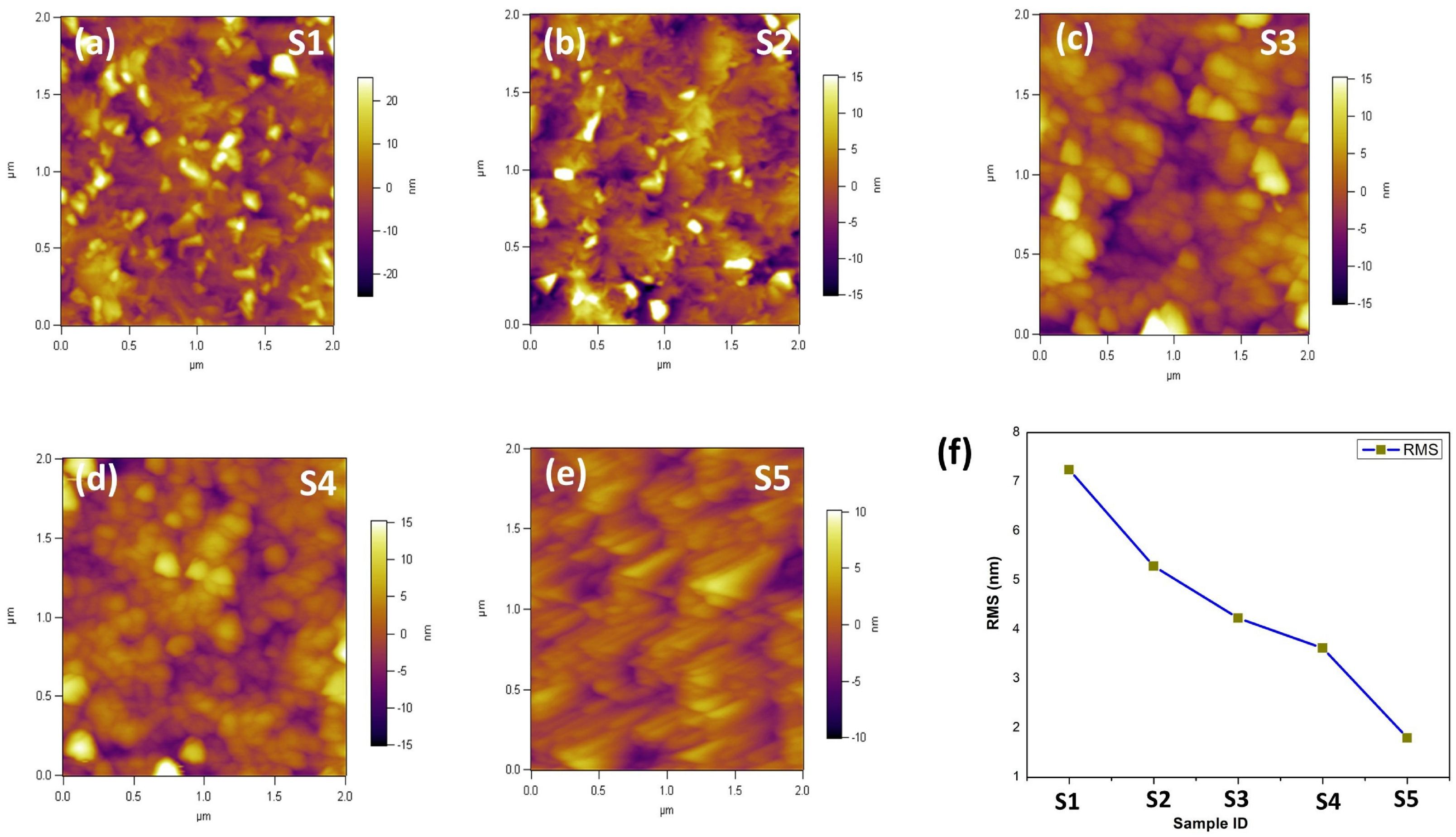
| S1 | 7.25 | 0.26171 | 2.47939 | 2.9623 |
| S2 | 5.29 | 0.24778 | 2.26872 | 2.84795 |
| S3 | 4.23 | 0.24285 | 2.0816 | 2.70323 |
| S4 | 3.63 | 0.24092 | 2.09423 | 2.68799 |
| S5 | 1.80 | 0.23355 | 1.41013 | 2.51486 |
Disclaimer/Publisher’s Note: The statements, opinions and data contained in all publications are solely those of the individual author(s) and contributor(s) and not of MDPI and/or the editor(s). MDPI and/or the editor(s) disclaim responsibility for any injury to people or property resulting from any ideas, methods, instructions or products referred to in the content. |
© 2026 by the authors. Licensee MDPI, Basel, Switzerland. This article is an open access article distributed under the terms and conditions of the Creative Commons Attribution (CC BY) license.
Share and Cite
Hayyak, R.; Ngo, T.S.; Iqbal, T.; Choi, M.-H.; Hong, S.-K.; Yeo, I.-G.; Na, M.; Eun, T.H. Effects of Substrate Polarity and Pre-Growth Treatments on Plasma-Assisted Molecular-Beam Epitaxy of β-Ga2O3 on 4° Off-Axis 4H-SiC. Crystals 2026, 16, 467. https://doi.org/10.3390/cryst16070467
Hayyak R, Ngo TS, Iqbal T, Choi M-H, Hong S-K, Yeo I-G, Na M, Eun TH. Effects of Substrate Polarity and Pre-Growth Treatments on Plasma-Assisted Molecular-Beam Epitaxy of β-Ga2O3 on 4° Off-Axis 4H-SiC. Crystals. 2026; 16(7):467. https://doi.org/10.3390/cryst16070467
Chicago/Turabian StyleHayyak, Raouf, Trong Si Ngo, Taswar Iqbal, Mee-Hi Choi, Soon-Ku Hong, Im-Gyu Yeo, Moonkyong Na, and Tai Hee Eun. 2026. "Effects of Substrate Polarity and Pre-Growth Treatments on Plasma-Assisted Molecular-Beam Epitaxy of β-Ga2O3 on 4° Off-Axis 4H-SiC" Crystals 16, no. 7: 467. https://doi.org/10.3390/cryst16070467
APA StyleHayyak, R., Ngo, T. S., Iqbal, T., Choi, M.-H., Hong, S.-K., Yeo, I.-G., Na, M., & Eun, T. H. (2026). Effects of Substrate Polarity and Pre-Growth Treatments on Plasma-Assisted Molecular-Beam Epitaxy of β-Ga2O3 on 4° Off-Axis 4H-SiC. Crystals, 16(7), 467. https://doi.org/10.3390/cryst16070467