

Advances in Homoepitaxial Mosaic Single-Crystal Diamond: Interface Stress Regulation

Abstract
1. Introduction
2. Homoepitaxial Growth: Progress and Limitations
3. Advances in Single-Crystal Diamond Mosaic Growth
3.1. Preparation and Pretreatment of Seed Crystals
3.2. Geometry and Process Design for Mosaic Growth
3.3. Parameter Control in Mosaic Growth
3.4. Innovative Methods for Mosaic Growth
4. Sources and Evolution of Interfacial Stress
4.1. Sources and Multiscale Characterization of Interfacial Stress
4.2. Stress Control via Process Optimization
4.3. Stress Control via Geometric Design
4.4. Theoretical Modeling of Interfacial Stress
5. Summary and Prospects
Author Contributions
Funding
Data Availability Statement
Conflicts of Interest
References
- Inyushkin, A.V.; Taldenkov, A.N.; Ralchenko, V.G.; Bolshakov, A.P.; Koliadin, A.V.; Katrusha, A.N. Thermal Conductivity of High Purity Synthetic Single Crystal Diamonds. Phys. Rev. B 2018, 97, 144305. [Google Scholar] [CrossRef]
- Wort, C.J.H.; Balmer, R.S. Diamond as an Electronic Material. Mater. Today 2008, 11, 22–28. [Google Scholar] [CrossRef]
- Umezawa, H. Recent Advances in Diamond Power Semiconductor Devices. Mater. Sci. Semicond. Process. 2018, 78, 147–156. [Google Scholar] [CrossRef]
- Shikata, S. Single Crystal Diamond Wafers for High Power Electronics. Diam. Relat. Mater. 2016, 65, 168–175. [Google Scholar] [CrossRef]
- Kasu, M. Diamond Epitaxy: Basics and Applications. Prog. Cryst. Growth Charact. Mater. 2016, 62, 317–328. [Google Scholar] [CrossRef]
- Achard, J.; Jacques, V.; Tallaire, A. Chemical Vapour Deposition Diamond Single Crystals with Nitrogen-Vacancy Centres: A Review of Material Synthesis and Technology for Quantum Sensing Applications. J. Phys. D Appl. Phys. 2020, 53, 313001. [Google Scholar] [CrossRef]
- Yang, H.; Ma, Y.; Dai, Y. Progress of Structural and Electronic Properties of Diamond: A Mini Review. Funct. Diam. 2022, 1, 150–159. [Google Scholar] [CrossRef]
- Ren, Y.; Li, X.; Lv, W.; Dong, H.; Cheng, Q.; Yue, F.; Woehrl, N.; Mendes, J.C.; Yang, X.; Li, Z. Recent Progress in Homoepitaxial Single-Crystal Diamond Growth via MPCVD. J. Mater. Sci. Mater. Electron. 2024, 35, 525. [Google Scholar] [CrossRef]
- Lu, F.X. Past, Present, and the Future of the Research and Commercialization of CVD Diamond in China. Funct. Diam. 2022, 2, 119–141. [Google Scholar] [CrossRef]
- Arnault, J.-C.; Saada, S.; Ralchenko, V. Chemical Vapor Deposition Single-Crystal Diamond: A Review. Phys. Status Solidi RRL 2022, 16, 2100354. [Google Scholar] [CrossRef]
- Zheng, Y.; Li, C.; Liu, J.; Wei, J.; Zhang, X.; Ye, H.; Ouyang, X. Chemical Vapor Deposited Diamond with Versatile Grades: From Gemstone to Quantum Electronics. Front. Mater. Sci. 2022, 16, 220590. [Google Scholar] [CrossRef]
- Schreck, M.; Gsell, S.; Brescia, R.; Fischer, M. Ion Bombardment Induced Buried Lateral Growth: The Key Mechanism for the Synthesis of Single Crystal Diamond Wafers. Sci. Rep. 2017, 7, 44462. [Google Scholar] [CrossRef] [PubMed]
- Mokuno, Y.; Chayahara, A.; Yamada, H.; Tsubouchi, N. Improving Purity and Size of Single-Crystal Diamond Plates Produced by High-Rate CVD Growth and Lift-off Process Using Ion Implantation. Diam. Relat. Mater. 2009, 18, 1258–1261. [Google Scholar] [CrossRef]
- Mokuno, Y.; Chayahara, A.; Soda, Y.; Horino, Y.; Fujimori, N. Synthesizing Single-Crystal Diamond by Repetition of High Rate Homoepitaxial Growth by Microwave Plasma CVD. Diam. Relat. Mater. 2005, 14, 1743–1746. [Google Scholar] [CrossRef]
- Kumar, R.; Nikhil, C.; Akash; Ramsubramanian, K.; Madana, V.S.T.; Arunachalam, N.; Ramachandra Rao, M.S. Investigation on the Epitaxial Lateral Outward Growth of Single Crystal Diamond Using MPCVD Growth Technique: Simulation Insights under High Pressure Conditions. Carbon 2026, 256, 121590. [Google Scholar] [CrossRef]
- Ren, Z.; Wang, C.; Zhang, J.; Zhu, Z.; Su, K.; Man, W.; Fu, Y.; Chen, J.; Li, J.; Zhu, W.; et al. Expansion Growth of <110>-Oriented Single Crystal Diamond. Appl. Surf. Sci. 2025, 703, 163439. [Google Scholar] [CrossRef]
- Qu, P.; Jin, P.; Zhou, G.; Wang, Z.; Wang, Z. Growth of Two-Inch Free-Standing Heteroepitaxial Diamond on Ir/YSZ/Si (001) Substrates via Laser-Patterned Templates. J. Semicond. 2024, 45, 090501. [Google Scholar] [CrossRef]
- Li, G.; Li, D.; Mu, C.; Wang, Q.; Lv, X.; Li, L.; Zou, G. Effect of Step-Flow Modulation on the Large-Size Single Crystal Diamond through Mosaic Growth. Funct. Diam. 2023, 3, 2279057. [Google Scholar] [CrossRef]
- Mu, C.; Lv, X.; Wang, Q.; Liu, X.; Fan, H.; Chen, J.; Li, L.; Zou, B.; Zou, G. Mosaic Growth and Characteristics of 2-Inch Single-Crystal Diamond. Funct. Diam. 2026, 6, 2620820. [Google Scholar] [CrossRef]
- Yamada, H.; Chayahara, A.; Mokuno, Y.; Tsubouchi, N.; Shikata, S.; Fujimori, N. Developments of Elemental Technologies to Produce Inch-Size Single-Crystal Diamond Wafers. Diam. Relat. Mater. 2011, 20, 616–619. [Google Scholar] [CrossRef]
- Yamada, H.; Chayahara, A.; Mokuno, Y.; Tsubouchi, N.; Shikata, S. Uniform Growth and Repeatable Fabrication of Inch-Sized Wafers of a Single-Crystal Diamond. Diam. Relat. Mater. 2013, 33, 27–31. [Google Scholar] [CrossRef]
- Mokuno, Y.; Chayahara, A.; Yamada, H. Synthesis of Large Single Crystal Diamond Plates by High Rate Homoepitaxial Growth Using Microwave Plasma CVD and Lift-off Process. Diam. Relat. Mater. 2008, 17, 415–418. [Google Scholar] [CrossRef]
- Yang, T.-I.; Chuang, C.-Y.; Huang, J.-B.; Ko, C.-J.; Wang, W.-L.; Chang, L. Enhanced Lateral Growth of Homoepitaxial (001) Diamond by Microwave Plasma Chemical Vapor Deposition with Nitrogen Addition. Coatings 2025, 15, 1256. [Google Scholar] [CrossRef]
- Ohmagari, S.; Yamada, H.; Tsubouchi, N.; Umezawa, H.; Chayahara, A.; Seki, A.; Kawaii, F.; Saitoh, H.; Mokuno, Y. Schottky Barrier Diodes Fabricated on Diamond Mosaic Wafers: Dislocation Reduction to Mitigate the Effect of Coalescence Boundaries. Appl. Phys. Lett. 2019, 114, 082104. [Google Scholar] [CrossRef]
- Zhu, X.; Liu, J.; Shao, S.; Tu, J.; Huang, Y.; Bi, T.; Chen, L.; Wei, J.; Kawarada, H.; Li, C. Evolution of Growth Characteristics around the Junction in the Mosaic Diamond. Diam. Relat. Mater. 2021, 120, 108640. [Google Scholar] [CrossRef]
- Field, J.E. The Properties of Natural and Synthetic Diamond; Academic Press: London, UK; San Diego, CA, USA; New York, NY, USA, 1992. [Google Scholar]
- Teraji, T. Chemical Vapor Deposition of Homoepitaxial Diamond Films. Phys. Status Solidi A 2006, 203, 3324–3357. [Google Scholar] [CrossRef]
- Li, X.; Wei, J.; Gao, J.; Wang, Y.; Ma, Y.; An, P.; Yu, S.; Zheng, K. Synergistic Control of Crystal Planes and Defects in CVD Single-Crystal Diamond: A Review of Growth Mechanisms and Frontier Applications. Coatings 2026, 16, 218. [Google Scholar] [CrossRef]
- Silva, F.; Achard, J.; Brinza, O.; Bonnin, X.; Hassouni, K.; Anthonis, A.; De Corte, K.; Barjon, J. High Quality, Large Surface Area, Homoepitaxial MPACVD Diamond Growth. Diam. Relat. Mater. 2009, 18, 683–697. [Google Scholar] [CrossRef]
- Xie, W.-L.; Lv, X.-Y.; Wang, Q.-L.; Li, L.-A.; Zou, G.-T. Relationship between the Spatial Position of the Seed and Growth Mode for Single-Crystal Diamond Grown with an Enclosed-Type Holder. Chin. Phys. B 2022, 31, 108106. [Google Scholar] [CrossRef]
- Widmann, C.J.; Hetzl, M.; Drieschner, S.; Nebel, C.E. Homoepitaxial Growth of High Quality (111)-Oriented Single Crystalline Diamond. Diam. Relat. Mater. 2017, 72, 41–46. [Google Scholar] [CrossRef]
- Mokuno, Y.; Chayahara, A.; Yamada, H.; Tsubouchi, N. Improvements of Crystallinity of Single Crystal Diamond Plates Produced by Lift-off Process Using Ion Implantation. Diam. Relat. Mater. 2010, 19, 128–130. [Google Scholar] [CrossRef]
- Janssen, G.; Giling, L.J. “Mosaic” Growth of Diamond. Diam. Relat. Mater. 1995, 4, 1025–1031. [Google Scholar] [CrossRef]
- Schermer, J.J.; de Theije, F.K.; Giling, L.J. Mosaic Growth of Diamond: A Study of Homoepitaxial Flame Deposition and Etching of {001}-Oriented Diamond Layers. J. Cryst. Growth 1996, 165, 387–401. [Google Scholar] [CrossRef][Green Version]
- Findeling-Dufour, C.; Gicquel, A. Study for Fabricating Large Area Diamond Single-Crystal Layers. Thin Solid Films 1997, 308–309, 178–185. [Google Scholar] [CrossRef]
- Tallaire, A.; Kasu, M.; Ueda, K.; Makimoto, T. Origin of Growth Defects in CVD Diamond Epitaxial Films. Diam. Relat. Mater. 2008, 17, 60–65. [Google Scholar] [CrossRef]
- Zhao, Y.; Guo, Y.; Lin, L.; Zheng, Y.; Hei, L.; Liu, J.; Wei, J.; Chen, L.; Li, C. Comparison of the Quality of Single-Crystal Diamonds Grown on Two Types of Seed Substrates by MPCVD. J. Cryst. Growth 2018, 491, 89–96. [Google Scholar] [CrossRef]
- Tallaire, A.; Achard, J.; Silva, F.; Brinza, O.; Gicquel, A. Growth of Large Size Diamond Single Crystals by Plasma Assisted Chemical Vapour Deposition: Recent Achievements and Remaining Challenges. Comptes Rendus Phys. 2013, 14, 169–184. [Google Scholar] [CrossRef]
- Mokuno, Y.; Kato, Y.; Tsubouchi, N.; Chayahara, A.; Yamada, H.; Shikata, S. A Nitrogen Doped Low-Dislocation Density Free-Standing Single Crystal Diamond Plate Fabricated by a Lift-off Process. Appl. Phys. Lett. 2014, 104, 252109. [Google Scholar] [CrossRef]
- Liu, N.; Yamada, H.; Yoshitaka, N.; Sugimoto, K.; Sun, R.; Kawai, K.; Arima, K.; Yamamura, K. Comparison of Surface and Subsurface Damage of Mosaic Single-Crystal Diamond Substrate Processed by Mechanical and Plasma-Assisted Polishing. Diam. Relat. Mater. 2021, 119, 108555. [Google Scholar] [CrossRef]
- Liu, N.; Sugawara, K.; Yoshitaka, N.; Yamada, H.; Takeuchi, D.; Akabane, Y.; Fujino, K.; Kawai, K.; Arima, K.; Yamamura, K. Damage-Free Highly Efficient Plasma-Assisted Polishing of a 20-mm Square Large Mosaic Single Crystal Diamond Substrate. Sci. Rep. 2020, 10, 19432. [Google Scholar] [CrossRef] [PubMed]
- Liu, N.; Wang, H.; Lei, L.; Jiang, H.; Zhang, Y.; Xiao, J.; Zhang, J.; Chen, X.; Xu, J. Highly Efficient Medium Vacuum UV-Assisted Polishing of Diamond via C-C Bond Breakage Stimulated Graphitization. Tribol. Int. 2025, 209, 110702. [Google Scholar] [CrossRef]
- Yu, Z.; Zhang, Z.; Zeng, Z.; Fan, C.; Gu, Y.; Shi, C.; Zhou, H.; Meng, F.; Feng, J. Atomic Surface of Diamond Induced by Novel Green Photocatalytic Chemical Mechanical Polishing with High Material Removal Rate. Int. J. Extrem. Manuf. 2025, 7, 025102. [Google Scholar] [CrossRef]
- Xin, Y.; Lu, J.; Hu, Y.; Huang, S.; Li, D.; Luo, Q.; Ke, C.; Xu, X. Research on High-Efficiency Mechanochemical Synergistic Polishing of Single Crystal Diamond Based on Anti-Oxidation Ceramic Grinding Wheels. Appl. Surf. Sci. 2025, 709, 163822. [Google Scholar] [CrossRef]
- Naamoun, M.; Tallaire, A.; Silva, F.; Achard, J.; Doppelt, P.; Gicquel, A. Etch-Pit Formation Mechanism Induced on HPHT and CVD Diamond Single Crystals by H2/O2 Plasma Etching Treatment. Phys. Status Solidi A 2012, 209, 1715–1720. [Google Scholar] [CrossRef]
- Ivanov, O.A.; Muchnikov, A.B.; Chernov, V.V.; Bogdanov, S.A.; Vikharev, A.L.; Butler, J.E. Experimental Study of Hydrogen Plasma Etching of (100) Single Crystal Diamond in a MPACVD Reactor. Mater. Lett. 2015, 151, 115–118. [Google Scholar] [CrossRef]
- Achard, J.; Tallaire, A.; Mille, V.; Naamoun, M.; Brinza, O.; Boussadi, A.; William, L.; Gicquel, A. Improvement of Dislocation Density in Thick CVD Single Crystal Diamond Films by Coupling H2/O2 Plasma Etching and Chemo-Mechanical or ICP Treatment of HPHT Substrates. Phys. Status Solidi A 2014, 211, 2264–2267. [Google Scholar] [CrossRef]
- Wei, Y.; Gao, J.; Zheng, K.; Ma, Y.; Zhi, J.; Jia, W.; Zheng, X.; Qu, S.; Zhou, B.; Yu, S. Microwave Hydrogen Plasma Etching on the Laser-Cut Surface of Single Crystal Diamond: Phases, Etching Morphology, Stress Evolution and the Effect of Etching on the Subsequent Homoepitaxial Growth. Diam. Relat. Mater. 2024, 143, 110937. [Google Scholar] [CrossRef]
- Sakamoto, K.; Tokunaga, D.; Itoh, S.; Hidai, H.; Matsusaka, S.; Omatsu, T.; Koyama, K.; Kim, S.-W.; Morita, N. Laser Slicing of a Diamond at the {100} Plane Using an Irradiation Sequence That Restricts Crack Propagation along the {111} Plane. Diam. Relat. Mater. 2023, 136, 110045. [Google Scholar] [CrossRef]
- Tallaire, A.; Barjon, J.; Brinza, O.; Achard, J.; Silva, F.; Mille, V.; Issaoui, R.; Tardieu, A.; Gicquel, A. Dislocations and Impurities Introduced from Etch-Pits at the Epitaxial Growth Resumption of Diamond. Diam. Relat. Mater. 2011, 20, 875–881. [Google Scholar] [CrossRef]
- Zhao, J.; Yang, Y.; Weng, C.; Zhu, W.; Lou, L.; Wang, G. The Quality of Epitaxial Lateral Overgrown Diamond on Substrate with Laser-Cut Holes of Varying Shapes and Side Orientations. Diam. Relat. Mater. 2024, 148, 111488. [Google Scholar] [CrossRef]
- Yamada, H.; Chayahara, A.; Mokuno, Y.; Umezawa, H.; Shikata, S.; Fujimori, N. Fabrication of 1 Inch Mosaic Crystal Diamond Wafers. Appl. Phys. Express 2010, 3, 051301. [Google Scholar] [CrossRef]
- Yamada, H.; Chayahara, A.; Mokuno, Y.; Kato, Y.; Shikata, S. A 2-in. Mosaic Wafer Made of a Single-Crystal Diamond. Appl. Phys. Lett. 2014, 104, 102110. [Google Scholar] [CrossRef]
- Muchnikov, A.B.; Radishev, D.B.; Vikharev, A.L.; Gorbachev, A.M.; Mitenkin, A.V.; Drozdov, M.N.; Drozdov, Y.N.; Yunin, P.A. Characterization of Interfaces in Mosaic CVD Diamond Crystal. J. Cryst. Growth 2016, 442, 62–67. [Google Scholar] [CrossRef]
- Zhang, W.; Sang, M.; Liu, C.; Zhu, Y.; Xie, Z.-X.; Zhou, W.; Yang, X.; Jiang, N.; Wang, Y. Fabrication of Seamless Mosaic Diamonds by Precise Controlling of the Crystallographic Orientations Followed by Surface Polishing. Opt. Mater. 2026, 174, 118012. [Google Scholar] [CrossRef]
- Wang, Q.; Li, G.; Li, D.; Lin, W.; Li, L.; Li, H.; Lv, X.; Zou, G. A Method for Improving the Growth Quality of Large-Area Single-Crystal Diamond Mosaic Splicing. Chinese Patent CN115874282A, 31 March 2023. [Google Scholar]
- Li, K.; Zhang, J.; Mo, P.; Chen, J.; Pan, X.; Chen, C. Optimizing Single Crystal Diamond Mosaic Growth: A Study on Seed Thickness Variation and Pre-Growth Treatment. J. Cryst. Growth 2025, 649, 127953. [Google Scholar] [CrossRef]
- Nad, S.; Gu, Y.; Asmussen, J. Growth Strategies for Large and High Quality Single Crystal Diamond Substrates. Diam. Relat. Mater. 2015, 60, 26–34. [Google Scholar] [CrossRef]
- Yamada, H.; Chayahara, A.; Mokuno, Y.; Horino, Y.; Shikata, S. Simulation of Temperature and Gas Flow Distributions in Region Close to a Diamond Substrate with Finite Thickness. Diam. Relat. Mater. 2006, 15, 1738–1742. [Google Scholar] [CrossRef]
- Feng, M.; Jin, P.; Meng, X.; Xu, P.; Wu, J.; Wang, Z. One-Step Growth of a Nearly 2 Mm Thick CVD Single Crystal Diamond with an Enlarged Surface by Optimizing the Substrate Holder Structure. J. Cryst. Growth 2023, 603, 127011. [Google Scholar] [CrossRef]
- Zhang, P.; Chen, W.; Zhang, L.; He, S.; Wang, H.; Yan, S.; Ma, W.; Guo, C.; Wang, Y. Evolution of High-Quality Homoepitaxial CVD Diamond Films Induced by Methane Concentration. Coatings 2021, 11, 888. [Google Scholar] [CrossRef]
- Issaoui, R.; Achard, J.; William, L.; Mehmel, L.; Pinault Thaury, M.-A.; Bénédic, F. Thick and Widened High Quality Heavily Boron Doped Diamond Single Crystals Synthetized with High Oxygen Flow under High Microwave Power Regime. Diam. Relat. Mater. 2019, 94, 88–91. [Google Scholar] [CrossRef]
- Chayahara, A.; Mokuno, Y.; Horino, Y.; Takasu, Y.; Kato, H.; Yoshikawa, H.; Fujimori, N. The Effect of Nitrogen Addition during High-Rate Homoepitaxial Growth of Diamond by Microwave Plasma CVD. Diam. Relat. Mater. 2004, 13, 1954–1958. [Google Scholar] [CrossRef]
- Tallaire, A.; Achard, J.; Silva, F.; Sussmann, R.S.; Gicquel, A. Homoepitaxial Deposition of High-Quality Thick Diamond Films: Effect of Growth Parameters. Diam. Relat. Mater. 2005, 14, 249–254. [Google Scholar] [CrossRef]
- Tallaire, A.; Collins, A.T.; Charles, D.; Achard, J.; Sussmann, R.; Gicquel, A.; Newton, M.E.; Edmonds, A.M.; Cruddace, R.J. Characterisation of High-Quality Thick Single-Crystal Diamond Grown by CVD with a Low Nitrogen Addition. Diam. Relat. Mater. 2006, 15, 1700–1707. [Google Scholar] [CrossRef]
- Achard, J.; Silva, F.; Tallaire, A.; Bonnin, X.; Lombardi, G.; Hassouni, K.; Gicquel, A. High Quality MPACVD Diamond Single Crystal Growth: High Microwave Power Density Regime. J. Phys. D Appl. Phys. 2007, 40, 6175. [Google Scholar] [CrossRef]
- Bolshakov, A.P.; Ralchenko, V.G.; Shu, G.; Dai, B.; Yurov, V.Y.; Bushuev, E.V.; Khomich, A.A.; Altakhov, A.S.; Ashkinazi, E.E.; Antonova, I.A.; et al. Single Crystal Diamond Growth by MPCVD at Subatmospheric Pressures. Mater. Today Commun. 2020, 25, 101635. [Google Scholar] [CrossRef]
- Lloret, F.; Araujo, D.; Eon, D.; del Pilar Villar, M.; Gonzalez-Leal, J.-M.; Bustarret, E. Influence of Methane Concentration on MPCVD Overgrowth of 100-Oriented Etched Diamond Substrates. Phys. Status Solidi A 2016, 213, 2570–2574. [Google Scholar] [CrossRef]
- Tang, Y.-H.; Golding, B. Stress Engineering of High-Quality Single Crystal Diamond by Heteroepitaxial Lateral Overgrowth. Appl. Phys. Lett. 2016, 108, 052101. [Google Scholar] [CrossRef]
- Li, F.; Zhang, J.; Wang, X.; Zhang, M.; Wang, H. Fabrication of Low Dislocation Density, Single-Crystalline Diamond via Two-Step Epitaxial Lateral Overgrowth. Crystals 2017, 7, 114. [Google Scholar] [CrossRef]
- Tallaire, A.; Brinza, O.; Mille, V.; William, L.; Achard, J. Reduction of Dislocations in Single Crystal Diamond by Lateral Growth over a Macroscopic Hole. Adv. Mater. 2017, 29, 1604823. [Google Scholar] [CrossRef] [PubMed]
- Shu, G.; Dai, B.; Ralchenkq, V.G.; Khomich, A.A.; Ashkinazi, E.E.; Bolshakov, A.P.; Bokova-Sirosh, S.N.; Liu, K.; Zhao, J.; Han, J.; et al. Epitaxial Growth of Mosaic Diamond: Mapping of Stress and Defects in Crystal Junction with a Confocal Raman Spectroscopy. J. Cryst. Growth 2017, 463, 19–26. [Google Scholar] [CrossRef]
- Shu, G.; Dai, B.; Ralchenko, V.G.; Bolshakov, A.P.; Khomich, A.A.; Ashkinazi, E.E.; Han, J.; Zhu, J. Growth of Three-Dimensional Diamond Mosaics by Microwave Plasma-Assisted Chemical Vapor Deposition. CrystEngComm 2018, 20, 198–203. [Google Scholar] [CrossRef]
- Wang, Y.; Zhu, T.; Liu, C.; Yang, K.; Yang, G.; Jiang, N. A Sandwich-Structured Optical-Grade Single-Crystal Diamond and Preparation Method Thereof. Chinese Patent CN118480863A, 13 August 2024. [Google Scholar]
- Wang, Q.; Bai, J.; Liu, L.; Lu, Y.; Tang, P.; Zhang, C.; Zhu, H.; Zheng, S. A Method for Homoepitaxial Mosaic Splicing of Single-Crystal Diamond and Interfacial Low-Stress Regulation. Chinese Patent CN115573042A, 6 January 2023. [Google Scholar]
- Ohmagari, S.; Yamada, H.; Umezawa, H.; Chayahara, A.; Teraji, T.; Shikata, S. Characterization of Free-Standing Single-Crystal Diamond Prepared by Hot-Filament Chemical Vapor Deposition. Diam. Relat. Mater. 2014, 48, 19–23. [Google Scholar] [CrossRef]
- Ohmagari, S.; Yamada, H.; Tsubouchi, N.; Umezawa, H.; Chayahara, A.; Tanaka, S.; Mokuno, Y. Large Reduction of Threading Dislocations in Diamond by Hot-Filament Chemical Vapor Deposition Accompanying W Incorporations. Appl. Phys. Lett. 2018, 113, 032108. [Google Scholar] [CrossRef]
- Wang, R.; Lin, F.; Niu, G.; Su, J.; Yan, X.; Wei, Q.; Wang, W.; Wang, K.; Yu, C.; Wang, H.-X. Reducing Threading Dislocations of Single-Crystal Diamond via in Situ Tungsten Incorporation. Materials 2022, 15, 444. [Google Scholar] [CrossRef] [PubMed]
- Wang, X.; Duan, P.; Cao, Z.; Liu, C.; Wang, D.; Peng, Y.; Xu, X.; Hu, X. Surface Morphology of the Interface Junction of CVD Mosaic Single-Crystal Diamond. Materials 2020, 13, 91. [Google Scholar] [CrossRef] [PubMed]
- Fischer, M.; Gsell, S.; Schreck, M.; Bergmaier, A. Growth Sector Dependence and Mechanism of Stress Formation in Epitaxial Diamond Growth. Appl. Phys. Lett. 2012, 100, 041906. [Google Scholar] [CrossRef]
- Sultana, M.; Karmakar, S.; Haque, A. N- and P-Type Doping of Diamonds: A Review. Mater. Sci. Semicond. Process. 2025, 186, 109024. [Google Scholar] [CrossRef]
- Lu, S.; Wang, H.; Zheng, Y.; Hu, X. First-Principles Analysis of Biaxial-Strain Reducing Ionization Energy in a Doped Diamond. Diam. Relat. Mater. 2026, 163, 113409. [Google Scholar] [CrossRef]
- Ichikawa, K.; Shimaoka, T.; Kato, Y.; Koizumi, S.; Teraji, T. Dislocations in Chemical Vapor Deposition Diamond Layer Detected by Confocal Raman Imaging. J. Appl. Phys. 2020, 128, 155302. [Google Scholar] [CrossRef]
- Guo, Y.; Liu, J.; Liu, J.; Zheng, Y.; Zhao, Y.; Yuan, X.; Guo, Z.; Hei, L.; Chen, L.; Wei, J.; et al. Comparison of α Particle Detectors Based on Single-Crystal Diamond Films Grown in Two Types of Gas Atmospheres by Microwave Plasma-Assisted Chemical Vapor Deposition. Int. J. Miner. Metall. Mater. 2020, 27, 703–712. [Google Scholar] [CrossRef]
- Shikata, S.; Tanno, T.; Teraji, T.; Kanda, H.; Yamada, T.; Kushibiki, J. Precise Measurements of Diamond Lattice Constant Using Bond Method. Jpn. J. Appl. Phys. 2018, 57, 111301. [Google Scholar] [CrossRef]
- Li, Z.; Cui, C.; Arteaga, O.; Bian, S.; Tong, H.; Lu, J.; Xu, X. Full-Field Measurement of Residual Stress in Single-Crystal Diamond Substrates Based on Mueller Matrix Microscopy. Measurement 2024, 234, 114790. [Google Scholar] [CrossRef]
- Pinero, J.C.; Fernandez, D.; Lloret, F.; Le Van-Jodin, L.; Chretien, J.; Masante, C.; Araujo, D. Inducing Controlled Blistering by Smart-CutTM Process in Semiconducting Diamond: A STEM Study. Appl. Surf. Sci. 2025, 681, 161570. [Google Scholar] [CrossRef]
- Tallaire, A.; Ouisse, T.; Lantreibecq, A.; Cours, R.; Legros, M.; Bensalah, H.; Barjon, J.; Mille, V.; Brinza, O.; Achard, J. Identification of Dislocations in Synthetic Chemically Vapor Deposited Diamond Single Crystals. Cryst. Growth Des. 2016, 16, 2741–2746. [Google Scholar] [CrossRef]
- Katamune, Y.; Inoshita, S.; Izumi, A.; Watanabe, K.; Teraji, T.; Koizumi, S. Cathodoluminescence of N-Type Diamond Films Grown by Hot-Filament Chemical Vapor Deposition: Effects of Hydrogen Concentration. Diam. Relat. Mater. 2026, 162, 113264. [Google Scholar] [CrossRef]
- Lu, C.; Li, Z.; Sang, X.; Fan, Z.; Xu, X.; Zhang, Y.; Xu, K.; Cheng, Y.; Zhao, J.; Zheng, J.-C.; et al. Stress-Driven Grain Boundary Structural Transition in Diamond by Machine Learning Potential. Small 2025, 21, 2409092. [Google Scholar] [CrossRef] [PubMed]
- Martyanov, A.; Tiazhelov, I.; Savin, S.; Voronov, V.; Konov, V.; Sedov, V. Synthesis of Polycrystalline Diamond Films in Microwave Plasma at Ultrahigh Concentrations of Methane. Coatings 2023, 13, 751. [Google Scholar] [CrossRef]
- Tallaire, A.; Achard, J.; Silva, F.; Gicquel, A. Effect of Increasing the Microwave Density in Both Continuous and Pulsed Wave Mode on the Growth of Monocrystalline Diamond Films. Phys. Status Solidi A 2005, 202, 2059–2065. [Google Scholar] [CrossRef]
- Xu, N.; Liang, K. An Epitaxial Healing Method for Single-Crystal Diamond Mosaic Seams Based on In-Situ High-Temperature Annealing Strengthening. Chinese Patent CN121781270A, 3 April 2026. [Google Scholar]
- Wang, X.; Wang, Y.; Han, S.; Guo, Z.; Peng, Y.; Xu, X. A Preparation Method for High-Quality Large-Size Single-Crystal Diamond Mosaic Splicing. Chinese Patent CN118814263A, 22 October 2024. [Google Scholar]
- Wang, Q.; Yan, H.; Lv, L.; Chang, H. A Processing Method for Edge Chamfering of Diamond Wafers. Chinese Patent CN118744373A, 8 October 2024. [Google Scholar]
- Jing, J.; Sun, F.; Wang, Z.; Ma, L.; Luo, Y.; Du, Z.; Zhang, T.; Wang, Y.; Xu, F.; Zhang, T.; et al. Scalable Production of Ultraflat and Ultraflexible Diamond Membrane. Nature 2024, 636, 627–634. [Google Scholar] [CrossRef] [PubMed]
- Liu, X.; Jiang, Y.; La, Y.; Liu, W. Phase-Field Modeling of Facet Growth of Diamond Using a Modified Anisotropic Coefficient of Interfacial Energy. Diam. Relat. Mater. 2024, 149, 111639. [Google Scholar] [CrossRef]
- Zhang, X.; Li, Y.; Liu, J.; Zhang, C.; Zhang, L. The Effect of Vacancy Defects on the Interfacial Thermal Resistance at the GaN/Diamond Interfaces: Molecular Dynamics Simulation. Model. Simul. Mater. Sci. Eng. 2025, 33, 045008. [Google Scholar] [CrossRef]



| Research Team | Year | Technical Approach | Maximum Lateral Size | Key Limitation |
|---|---|---|---|---|
| Mokuno et al. (AIST, Japan) | 2005 | Repeated high-rate growth on a closed substrate holder [14]. | Thickness: 10 mm (lateral dimensions only 5 × 5 mm2) | Excellent vertical thickening capability, but lateral dimensions remain limited |
| Mokuno et al. (AIST, Japan) | 2009 | Lift-off process combined with lateral growth for diameter expansion [13]. | 12.6 × 13.3 mm2 (half-inch) | Limited lateral expansion (from 9 mm to 12.6 mm) |
| Zou Guangtian’s team (Jilin University) | 2022 | Optimization of seed crystal spatial positioning and growth mode using a closed substrate holder [30]. | 8.6 × 8.6 mm2 (~51% area increase) | Improved uniformity, but no independent breakthrough in lateral size achieved |
| Zhang et al. (Xidian University) | 2025 | Lateral growth on (110) crystal plane with optimized CH4/O2 ratio [16]. | 7.03 × 8.12 mm2 (~75% area increase) | Size remains at the millimeter scale, still falling short of the inch scale |
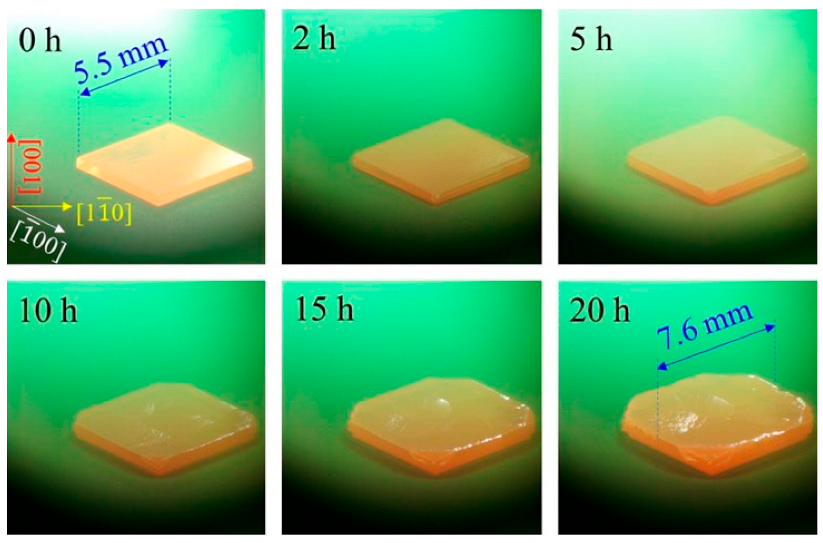
| Yang et al. (NYCU, Taiwan) | 2025 | Nitrogen-assisted MPCVD enhancing (001) lateral growth [23]. | 7.6 mm (~1.6-fold area increase) | Limited lateral expansion; absolute size remains at the millimeter scale |
| Kumar et al. (IIT Madras) | 2026 | Lateral outward growth under high-pressure MPCVD conditions (165 Torr) [15]. | 12.56 × 12.59 mm2 (59% area increase) | Limited lateral expansion; no order-of-magnitude breakthrough in absolute size |
| Polishing Technique | Core Mechanism | MRR | Surface Roughness | Sub-Surface Damage |
|---|---|---|---|---|
| Mechanical Polishing (MP) | High-speed cutting with diamond grit [40]. | - | >1 nm | Severe (scratches, amorphous layer) |
| Chemical Mechanical Polishing (CMP) | Synergistic action of oxidant and abrasive [45]. | ~300 nm/h | 0.3–0.5 nm | Low |
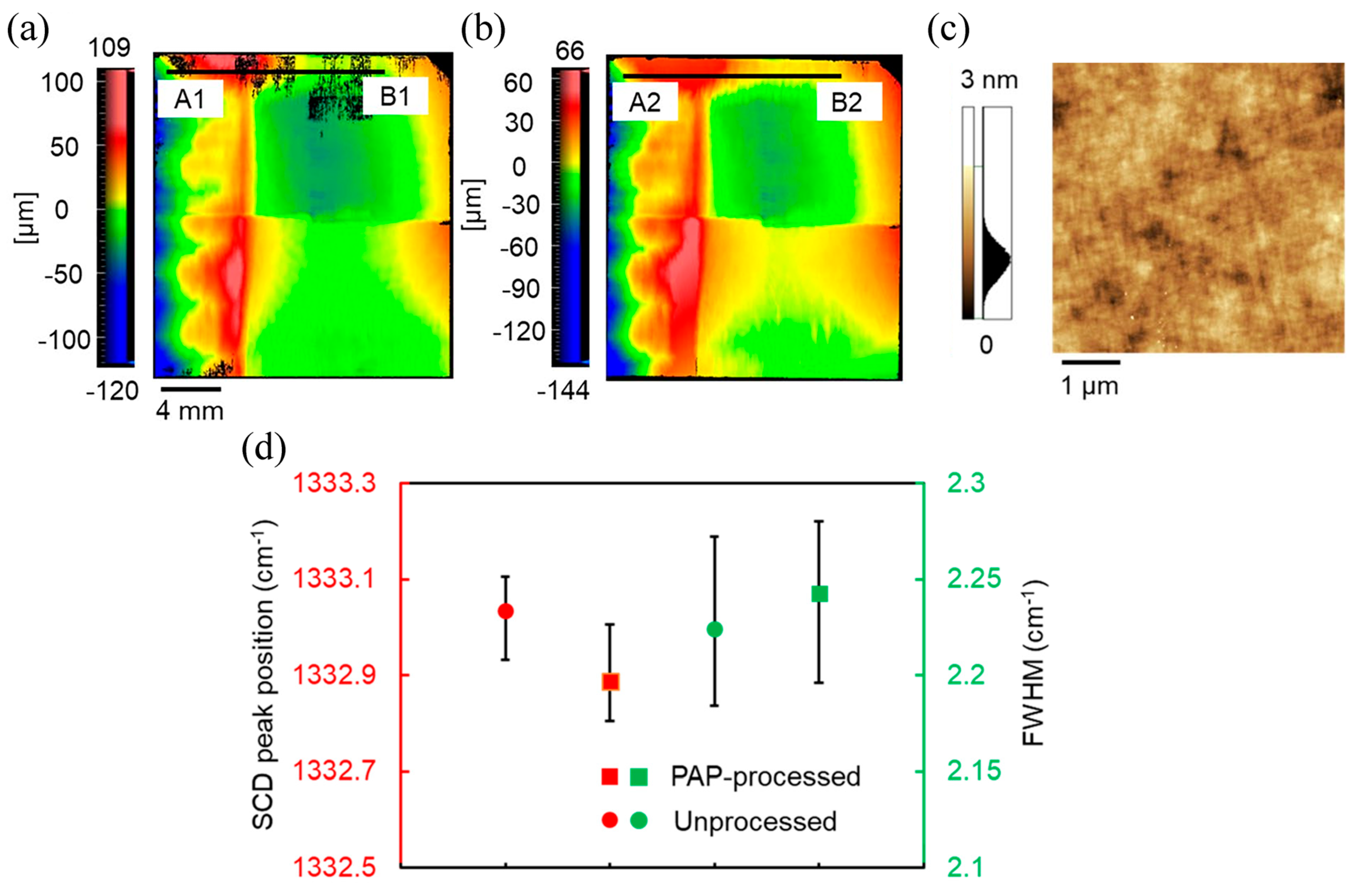
| Plasma-Assisted Polishing (PAP) | Ar/O2 plasma irradiation + removal by quartz glass [41]. | 13.3 μm/h | 0.4–0.5 nm Sq | None |
| Medium-Vacuum UV-Assisted Polishing | UV irradiation-induced graphitization + removal by quartz glass [42]. | 8.0 μm/h | <0.5 nm | None |
| UV Photocatalytic-Assisted CMP | TiO2 + PB/H2O2 ·OH oxidation + abrasive removal [43]. | 1168 nm/h | 0.079 nm Sa | Very thin (0.66 nm) |
| Mechanochemical Synergistic Wheel Polishing | Active metal-catalyzed graphitization + wheel removal [44]. | 8.186 μm/h | 0.721 nm Sa | Very thin amorphous layer |
| Regulation Strategy | Specific Method | Regulation Mechanism | Typical Effect |
|---|---|---|---|
| Process optimization | Optimize the lateral-to-vertical growth rate ratio λ (λ > 1) | Promote dislocation bending and lateral propagation rather than vertical extension to the surface [51]. | Dislocation density reduced from 6 × 10⁶ to 3 × 105 cm−2 (20-fold reduction); tensile stress reduced by ~0.14 GPa [51] |
| Process optimization | Addition of appropriate amount of O2 + pulsed growth | O2 introduces OH radicals that selectively etch non-diamond phases [62]; pulsed mode interrupts continuous stress accumulation through alternating growth–etching cycles [92]. | Improved crystal quality, reduced Raman FWHM, and decreased intrinsic stress [62,92]. |
| Process optimization | In situ high-temperature annealing | Sufficient atomic diffusion across the interface during in situ annealing at elevated temperatures eliminates residual stress [93]. | Electrical, thermal, and mechanical properties of the healed interface approach those of bulk single crystals [93] |
| Geometric design | SiO2 mask blocking | After the first mosaic growth, a SiO2 mask is deposited at the seam; defects beneath the mask are “bypassed” by the laterally overgrowing epitaxial layer [94]. | Effectively prevents defects and stress at the seam from propagating vertically into subsequent epitaxial layers [94]. |
| Geometric design | Seed crystal edge chamfering | Chamfering or rounding the edges of seed crystals to disperse mechanical stress [95]. | Reduces the edge stress concentration factor, lowering the risk of edge chipping and cracking [95]. |
| Geometric design | 60° interface angle | The inclined interface alters the manner in which lateral growth fronts meet, preventing direct collision perpendicular to the growth surface [54]. | The interface is the smoothest, with the lowest residual stress of only 0.42 GPa [54] |
| Geometric design | Rectangular holes (aspect ratio > 1) | The longer side provides a longer stable extension distance, maintaining an ordered step-flow [51]. | More effective than square holes in reducing stress and dislocation density [51]. |
| Strain engineering | 3% biaxial tensile strain | Modulates the band structure of diamond and the electronic states of dopant atoms [82]. | B-doping ionization energy decreases from 0.33 eV to 0.12 eV (a 64% reduction), and P-doping decreases from 0.56 eV to 0.35 eV (a 37% reduction) [82]. |
| Flexible connection | SiC nanowire interlayer | Nanowires penetrate the diamond crystal to form a flexible transition layer; their deformability provides additional degrees of freedom for stress release [75]. | With a coefficient of thermal expansion (CTE) intermediate between that of diamond and metal, it can effectively mitigate the accumulation of thermal mismatch stress (theoretical prediction) [75]. |
Disclaimer/Publisher’s Note: The statements, opinions and data contained in all publications are solely those of the individual author(s) and contributor(s) and not of MDPI and/or the editor(s). MDPI and/or the editor(s) disclaim responsibility for any injury to people or property resulting from any ideas, methods, instructions or products referred to in the content. |
© 2026 by the authors. Licensee MDPI, Basel, Switzerland. This article is an open access article distributed under the terms and conditions of the Creative Commons Attribution (CC BY) license.
Share and Cite
Rong, R.; Bai, J. Advances in Homoepitaxial Mosaic Single-Crystal Diamond: Interface Stress Regulation. Crystals 2026, 16, 448. https://doi.org/10.3390/cryst16070448
Rong R, Bai J. Advances in Homoepitaxial Mosaic Single-Crystal Diamond: Interface Stress Regulation. Crystals. 2026; 16(7):448. https://doi.org/10.3390/cryst16070448
Chicago/Turabian StyleRong, Rong, and Jie Bai. 2026. "Advances in Homoepitaxial Mosaic Single-Crystal Diamond: Interface Stress Regulation" Crystals 16, no. 7: 448. https://doi.org/10.3390/cryst16070448
APA StyleRong, R., & Bai, J. (2026). Advances in Homoepitaxial Mosaic Single-Crystal Diamond: Interface Stress Regulation. Crystals, 16(7), 448. https://doi.org/10.3390/cryst16070448