Article

Spatially Confined Crystallization of Patterned MAPbBr3−xClx Microcrystals

State Key Laboratory of Bioinspired Interfacial Materials Science, Institute of Functional Nano & Soft Materials (FUNSOM), Soochow University, Suzhou 215123, China
*
Authors to whom correspondence should be addressed.
These authors contributed equally to this work.
Crystals 2026, 16(6), 361; https://doi.org/10.3390/cryst16060361
Submission received: 1 April 2026 / Revised: 20 May 2026 / Accepted: 22 May 2026 / Published: 26 May 2026

Abstract

Patterned lead-halide perovskite microstructures are promising for integrated optoelectronics, photonics, and polarization-sensitive devices, but the practical growth behavior of compositionally tunable microcrystals under simple static confinement remains insufficiently understood. Here, we investigate template-assisted confined crystallization of MAPbBr3 and MAPbBr3−xClx microstructures using patterned polydimethylsiloxane (PDMS) stamps. MAPbBr3 was first examined as a reference system to evaluate pattern transfer, morphology, substrate compatibility, and characteristic growth imperfections. Periodic microstructures with template spacings from 0.8 to 10 μm were obtained on Si/SiO2, ITO, PDMS, and MAPbBr3 macrocrystal substrates. Static stamping creates strong edge–center morphological divergence: thick patterned microcrystals and coalesced domains formed preferentially near the sample edges, whereas thinner isolated microcrystal arrays were more common in central regions. XRD, AFM, SEM, SAED, EDX, HRTEM, PL microscopy, and TRPL analyses show that the method can generate well-crystallized and optically active perovskite domains while also producing multidomain aggregates, incomplete pattern transfer, pressure-induced wrinkling, and nanoscale secondary crystallites. Extension to MAPbBr3−xClx demonstrates that patterned mixed-halide microstructures can be obtained with composition-dependent structural and optical properties. Nevertheless, XRD, EDX, PL, and TRPL results indicate that Cl-rich samples are not fully described by a simple homogeneous solid-solution model, likely involving compositionally heterogeneous crystallization and a Br-rich emissive component. Preliminary MAPbCl3-on-MAPbBr3 experiments further show that PDMS-confined patterning can be coupled with substrate-mediated halide exchange or interfacial recrystallization. Overall, static PDMS-confined crystallization is established as a simple exploratory platform for producing diverse patterned perovskite microstructures. This approach is well-suited for the manual selection of suitable crystals and the fabrication of individual microdevices; however, improved control over pressure, mass transport, nucleation localization, and composition will be required when the uniformity of produced patterned microcrystals is desired.

1. Introduction

Organic–inorganic hybrid lead halide perovskites have emerged as an important class of solution-processable semiconductors because they combine strong light absorption, direct and tunable bandgaps, high charge-carrier mobility, long carrier diffusion lengths, and comparatively high defect tolerance [1,2]. These properties have enabled their use in solar cells, light-emitting diodes, lasers, photodetectors, and X-ray detectors, making crystallization control a central issue for both fundamental studies and device-oriented materials engineering [1,3,4]. Compared with polycrystalline thin films, perovskite single crystals and single-crystal-like microstructures are particularly attractive because they reduce the influence of grain boundaries and provide clearer relationships among crystal structure, chemical composition, defect density, and optoelectronic response [1,2,5,6,7].
Compositional engineering is one of the most direct strategies for tuning the optical and electronic properties of halide perovskites [1]. In mixed-halide systems such as MAPbBr3−xClx, substitution of Br by Cl increases the bandgap and enables composition-dependent optical responses across the visible spectral range [1,8,9,10,11]. This tunability is especially important for wavelength-selective photodetection, light emission, and other bandgap-engineered optoelectronic applications [1,10]. Mixed-halide perovskite single crystals have been used to realize narrowband photodetectors with composition-dependent spectral response, demonstrating the functional importance of combining halide-composition control with high crystalline quality [1]. However, mixed-halide crystallization is not always a simple linear translation of precursor stoichiometry into crystal composition because the actual Br/Cl ratio in solution-grown MAPbBr3−xClx crystals can deviate from the nominal precursor ratio under certain growth conditions [1]. Compositionally graded or layered perovskite single crystals have also been fabricated by solution-processed epitaxial growth, highlighting the importance of lattice matching, halide diffusion, and solvent-dependent growth behavior in multicomponent perovskite systems [3].
In parallel with compositional control, patterned crystallization of perovskites has become increasingly important for integrated optoelectronics, photonics, micro-LEDs, image sensors, and polarization-sensitive photodetectors [4,7,12,13,14,15,16,17,18,19]. Patterned perovskite architectures can define active device regions, introduce structural anisotropy, guide light–matter interactions, and enable spatially organized microcrystal or microwire arrays [4,17]. Hydrophobic/hydrophilic substrate patterning has been used to localize precursor droplets within predefined wetting regions and thereby promote site-selective growth of perovskite single-crystal arrays, including halogen-composition-controlled crystals with emission tunable across the visible region [10]. Patterned homoepitaxial growth on MAPbBr3 single-crystal substrates provides excellent control over crystal position, morphology, and orientation, and has enabled ordered single-crystal arrays for light-emitting-device applications [7]. Geometrically confined lateral crystal growth using a rolling PDMS mould has produced wafer-scale, highly aligned single-crystal perovskite patterned thin films, demonstrating the power of confinement and directional growth for scalable patterning [17]. Solution-based epitaxial nanopatterning has further shown that surface patterns on perovskite monocrystalline thin films can modify photoluminescence intensity and recombination dynamics, emphasizing the functional relevance of patterned perovskite surfaces [20].
PDMS-based confinement provides a particularly accessible route for perovskite microcrystallization because it can control solvent evaporation, restrict vertical crystal growth, and generate smooth microcrystals with thicknesses closer to device-relevant length scales than millimeter-scale bulk crystals [2]. Flat PDMS stamping has been used to grow non-patterned single microcrystals of several halide perovskites, including mixed-halide MAPbBr1.5Cl1.5 and MAPbBr2.25Cl0.75, but in that method, the PDMS surface was flat, and the resulting microcrystals were not periodically patterned [2]. Patterned arrays of mixed-halide perovskite microplate crystals have also been demonstrated, but the individual crystals were small, approximately several micrometers in lateral size, and their surfaces were not topographically patterned [21]. Sequential crystallization in PDMS microchannels has been used to fabricate lateral MAPbI3–MAPbBr3 microwire heterojunctions with strong polarization-sensitive photodetection, showing that confined perovskite growth can be extended toward spatially organized multicomponent structures [4]. Nevertheless, the static PDMS-confined growth of compositionally tunable MAPbBr3−xClx microcrystals with transferred surface patterns remains a distinct and insufficiently characterized crystallization problem [2,4].
Importantly, many previous studies of patterned or confined perovskite microcrystals have focused mainly on device fabrication and device performance, for which manually selected individual crystals or selected patterned regions were typically sufficient [2,4,7]. As a result, comparatively less practical information has been provided about the actual surface coverage, spatial uniformity, dimensional variation, morphological diversity, and composition distribution of the full population of microstructures produced by simple static PDMS-confined crystallization [2]. This device-oriented perspective may unintentionally give the impression that static PDMS stamping provides a straightforward route to uniformly patterned microcrystal arrays. In the present work, we therefore place specific emphasis on these practical growth outcomes, including edge–center morphology divergence, pattern-transfer fidelity, local defects, compositional heterogeneity, and the limitations of the method, while also demonstrating its usefulness as an exploratory platform for patterned mixed-halide perovskite microcrystallization.
Here, we investigate template-assisted confined crystallization of patterned MAPbBr3−xClx microcrystals using static PDMS stamps as spatial templates. By emphasizing both successful pattern transfer and the limitations arising from stochastic nucleation, edge–center growth divergence, local defects, and non-ideal mixed-halide incorporation, this work provides a realistic assessment of static PDMS-confined crystallization as an exploratory platform for compositionally tunable patterned perovskite microstructures.

2. Materials and Methods

2.1. Materials

N,N-Dimethylformamide (DMF, 99.9%), lead (II) bromide (PbBr2, 99%), and lead (II) chloride (PbCl2, 99%) were purchased from Aladdin (Shanghai, China). Methylammonium bromide (MABr, 99%) was purchased from J&K Scientific Ltd. (Beijing, China). Methylammonium chloride (MACl, 99%) was purchased from Adamas (Shanghai, China). Dimethyl sulfoxide (DMSO, 99.9%) was purchased from Macklin Biochemical Co., Ltd. (Shanghai, China). Chlorobenzene was purchased from Xiya reagent (Linyi, China). Polydimethylsiloxane (PDMS) prepolymer Sylgard 184 and its curing agent were purchased from Dow Corning (Midland, MI, USA). All reagents and solvents were used as received without further purification.

2.2. Fabrication of Patterned PDMS Templates

To prepare the PDMS precursor, a silicone elastomer and its curing agent were combined at a 10:1 volume ratio. This mixture was continuously stirred in a beaker until it formed a homogeneous, white, viscous solution. To eliminate air bubbles that might hinder the subsequent curing process and to prevent overflow, the solution was transferred to a large-diameter crystallization dish and degassed under vacuum for 30 min.
Meanwhile, a DVD template (larger than 2 × 2 cm2) was cut, delaminated, and cleaned sequentially with ethanol and deionized water to remove dyes, dust, and polycarbonate residues, followed by drying with nitrogen gas. The prepared DVD template (or alternatively commercial PET master gratings with periods of 2 µm, 3.3 µm, and 10 µm) was placed on a hotplate at 80 °C. The degassed PDMS solution was poured onto the template and allowed to spread naturally. After curing for 30 min, the fully solidified, non-tacky elastic template was gently peeled from the master mold, revealing distinct structurally colored stripes when viewed at an angle. Finally, the PDMS template was subjected to UV–ozone treatment for 30 min to render the surface hydrophilic, and subsequently trimmed into squares of the desired dimensions.

2.3. Unconfined Growth of MAPbBr3 Microcrystals

For unconfined crystallization, PbBr2 and MABr powders were weighed in a 1:1 molar ratio and dissolved in a mixed solvent system of DMF and DMSO (3:1 by volume) to obtain 1 M MAPbBr3 precursor solution. This mixture was stirred at room temperature until a clear, homogeneous precursor solution was formed. Next, 150 µL of this MAPbBr3 precursor solution was spin-coated onto a silicon substrate at 2000 rpm for 20 s. During the final 10 s of the spin-coating process, 40 µL of chlorobenzene was rapidly dispensed onto the spinning substrate to serve as an antisolvent. Finally, the sample was annealed at 100 °C for 5 min to complete the crystallization process.

2.4. Preparation of Substrates and MAPbBr3 Single-Crystal Supports

Target substrates, including silicon wafers, ITO-coated glass, and plain PDMS, were cleaned sequentially via ultrasonication in detergent, deionized water, acetone, and isopropanol. A subsequent 30 min UV–ozone treatment was applied to enhance their surface wettability.
Macroscopic MAPbBr3 single crystals were grown by placing a glass vial containing the 1 M MAPbBr3 precursor solution in an 80 °C oil bath for 3 h. Following growth, the crystals were rinsed with isopropanol, dried under a nitrogen flow, and stored in sealed vials. After crystal growth, the grown bulk MAPbBr3 single crystals were further characterized by powder XRD, absorption/Tauc analysis, PL spectroscopy, and TRPL measurements to verify their crystal quality (Figure S1). The resulting structural and optical properties are comparable to those reported for high-quality MAPbBr3 bulk single crystals in the literature [22]. To prepare a flat supporting substrate from these bulk crystals, a crystal was embedded in a thick layer of uncured PDMS precursor (Sylgard 184, 10:1 ratio) and the assembly was cured on a hotplate at 80 °C for 30 min. Demolding yielded a supported MAPbBr3 single-crystal substrate with an exposed flat top surface.

2.5. Confined Growth of Patterned MAPbBr3−xClx Microcrystals

A 1 M MAPbBr3 precursor solution was prepared by dissolving equimolar amounts (1:1 ratio) of MABr and PbBr2 in DMF. Similarly, a 1 M MAPbCl3 precursor solution was prepared by dissolving equimolar amounts of MACl and PbCl2 in DMSO. Both solutions were stirred at room temperature for 3 h and then filtered through 0.2 µm polytetrafluoroethylene (PTFE) membrane filters.
Two solvent systems were mainly employed to prepare mixed-halide precursor solutions.
For the DMF/DMSO mixed-solvent system, the desired mixed-halide precursor compositions (MAPbBr0.5Cl2.5, MAPbBrCl2, MAPbBr1.5Cl1.5, and MAPbBr2Cl) were obtained by mixing 1 M MAPbBr3 in DMF and 1 M MAPbCl3 in DMSO solutions in specific volumetric ratios (0.5:2.5, 1:2, 1.5:1.5, and 2:1, respectively).
For the pure DMSO system, the desired mixed-halide precursor compositions (MAPbBr0.5Cl2.5, MAPbBrCl2, MAPbBr1.5Cl1.5, MAPbBr2Cl, and MAPbBr2.5Cl0.5) were prepared by mixing 1 M MAPbBr3 in DMSO and 1 M MAPbCl3 in DMSO solutions in specific volumetric ratios (0.5:2.5, 1:2, 1.5:1.5, 2:1, and 2.5:0.5, respectively).
To perform confined crystallization, 2 µL of the target precursor solution was drop-cast onto the cleaned substrate and immediately covered with a pre-patterned PDMS template. Unless otherwise specified, a weighting block was used to apply a uniform external pressure of approximately 8 kPa. The entire substrate–solution–PDMS assembly was then transferred to a heating platform set to 60 °C to allow crystal growth to complete.
As illustrated in Figure S2, the pressure is applied by placing a flat weight directly on top of the sample stack. The stack consists of a PDMS layer firmly attached to a glass substrate, which helps ensure effective load transfer and improves the uniformity of the applied pressure. A 50 g weight is used to provide a constant vertical load, corresponding to an applied pressure of approximately 8 kPa on the sample. The load is transmitted through the PDMS layer to the underlying perovskite.

2.6. Characterization

The surface morphologies and elemental distributions of the patterned microcrystals were examined using an optical microscope (Leica, Wetzlar, Germany) and a scanning electron microscope (SEM, Zeiss G500, Oberkochen, Germany) equipped with an energy-dispersive X-ray spectroscopy (EDX) detector (Oxford Instruments, Abingdon, UK). SEM imaging was conducted at an acceleration voltage of 10 kV in high-vacuum mode. EDX analyses were performed at the same acceleration voltage to determine the chemical compositions of the films. Both planar and tilted-view EDX measurements were employed to assess the three-dimensional elemental distribution within the crystals. The surface topography and depth profiles of the patterned stripes were characterized via atomic force microscopy (AFM) using a Cypher ES (Asylum Research) system in tapping mode under ambient conditions (Oxford Instruments Asylum Research, Santa Barbara, CA, USA), utilizing Multi75Al-G probes with a resonance frequency of approximately 75 kHz (BudgetSensors, Sofia, Bulgaria). The structural characterization was performed using a transmission electron microscope (TALOS 200X) (Thermo Fisher Scientific, Eindhoven, The Netherlands). The phase purity and crystal structure of the perovskite architectures were analyzed by X-ray diffraction (XRD) using an Empyrean diffractometer equipped with Cu Kα radiation and a PIXcel3D 2 × 2 area detector (Malvern Panalytical, Almelo, The Netherlands). The diffractometer was operated at 40 kV and 40 mA, with diffraction patterns collected over a 2θ range of 10–50°. Optical properties were systematically evaluated at room temperature. Fluorescence images in the dark field were recorded by a Leica fluorescence optical microscope with the excitation of a 405 nm laser (Leica Microsystems, Wetzlar, Germany). Ultraviolet-visible-near-infrared (UV-Vis-NIR) absorption spectra were collected using a Shimadzu UV-3600 spectrophotometer equipped with an integrating sphere, enabling the determination of continuous bandgap shifts as a function of halide composition (Shimadzu Corporation, Kyoto, Japan). Finally, steady-state photoluminescence (PL) spectra were acquired using a Fluoromax-4 fluorescence spectrophotometer (HORIBA Scientific, Kyoto, Japan). Excitation was provided by a continuous xenon lamp (Xe 900, Edinburgh Instruments Ltd., Livingston, UK)) at 350 nm, with the excitation and detection slit widths set to 5 nm and 1.75 nm, respectively, and the spectra were recorded using a 2 nm step size. TRPL measurements and decay fitting were carried out using a transient electroluminescence and photoluminescence temperature-dependent measurement system (QUANTAURUS-Tau) (Hamamatsu Photonics, Hamamatsu, Japan).

3. Results and Discussion

This work focuses on the confined microcrystallization of multi-component lead-halide perovskites using static PDMS patterns as spatial templates. Beyond introducing a more compositionally complex crystallization system, this study also clarifies several practical aspects of the reference MAPbBr3 patterned microcrystal system that have received limited attention in previous reports.

3.1. The Choice and Justification of Experimental Design

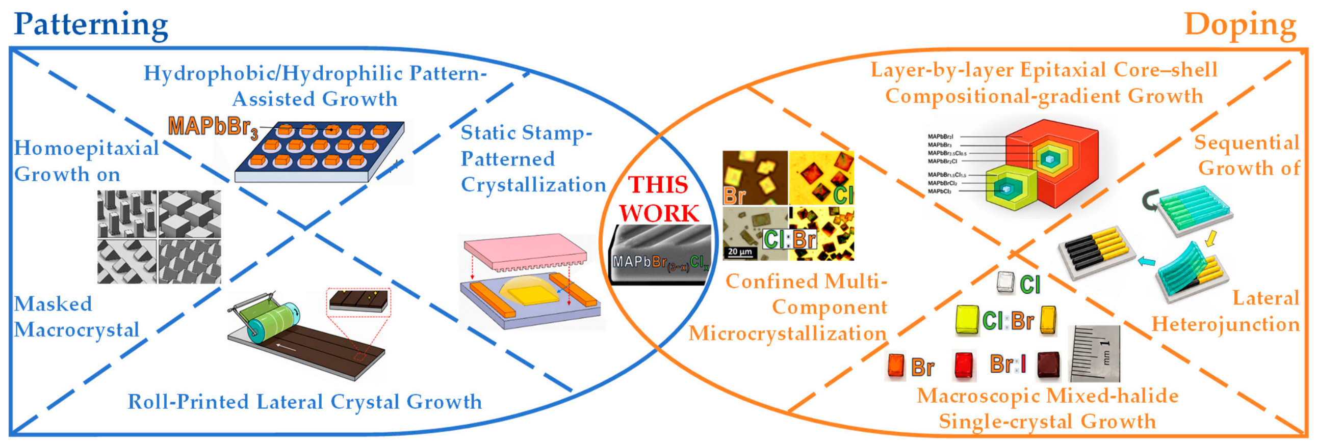
The present study was designed at the intersection of two related but only partially overlapping research directions: mixed-halide perovskite crystallization and patterned/confined perovskite microcrystal growth (Figure 1). Mixed-halide perovskites have been widely explored in bulk single-crystal form, where Br/Cl or I/Br substitution enables composition-dependent optical responses, although the actual crystal composition can deviate from the nominal precursor ratio under certain growth conditions [1]. Compositionally graded or layered perovskite single crystals have also been produced by solution-processed epitaxial growth [3], while sequential precursor replacement in PDMS microchannels has been used to fabricate lateral perovskite microwire heterojunctions [4]. Most relevant to the present work, mixed-halide compositions have previously been obtained as non-patterned microcrystals by flat PDMS-stamped crystallization [2].
In parallel, several strategies have been developed for positioning or patterning perovskite microstructures, each differing in experimental complexity, substrate requirements, scalability, and degree of crystallization control. Hydrophobic/hydrophilic substrate patterning can localize precursor droplets within predefined wetting regions and thereby promote site-selective nucleation of individual microcrystals, but it requires lithographic patterning, surface chemical modification, and careful control of wetting and evaporation conditions [10]. Patterned homoepitaxial growth on perovskite single-crystal substrates provides excellent control over crystal position, morphology, and orientation, but relies on advanced microfabrication and requires an appropriate perovskite single crystal as the homoepitaxial substrate [7]. Geometrically confined lateral crystal growth using a rolling PDMS mould offers an impressive route to large-area, highly aligned single-crystal perovskite patterned thin films, although it involves a specialized printing geometry, elevated substrate temperature, and careful optimization of rolling speed, solvent evaporation, and confinement conditions [17]. By contrast, sandwiching a precursor solution between a static patterned PDMS stamp and a target substrate provides a simpler and experimentally accessible route to patterned microcrystals and microrod arrays [20]. This approach was selected here because it enables exploratory perovskite growth on different substrates, facilitates the identification and manual selection of individual microstructures for characterization or device-oriented studies, and provides a simple static reference for our ongoing studies of heterogeneous mixed-halide perovskite crystallization with PDMS-based microchannels, where solution flow may offer additional control over composition, nucleation, and growth.
Previous studies using static PDMS-stamping approaches have often focused on fabricating and testing devices based on manually selected individual microstructures [19,20,23,24,25,26]. For this purpose, static confinement of the perovskite precursor solution between a substrate and a PDMS stamp is highly convenient. However, such a device-focused perspective may unintentionally create the impression that static PDMS-confined crystallization provides a straightforward route to highly uniform patterned microcrystals. Indeed, this was also our initial assumption when we began the present study. Our observations show that this is not necessarily the case: the method produces a wide variety of crystal morphologies, dimensions, degrees of pattern registration, and local growth outcomes (Figure S3). Recognizing this variability does not diminish the value of previously reported microdevices or patterned perovskite studies. Rather, it provides important practical context for researchers and helps clarify that static PDMS-confined crystallization is most appropriate for exploratory growth studies and for the manual selection of high-quality individual microcrystals for device fabrication.
This experimental choice also defines the type of morphological analysis that can reasonably be performed. Unlike approaches based on lithographically defined nucleation sites, hydrophilic/hydrophobic micropatterns, or patterned masks for homoepitaxial growth, the static PDMS-stamping geometry used here does not prescribe the positions at which nuclei form. Nucleation, therefore, occurs stochastically within the confined precursor film, and subsequent crystal growth is governed by local variations in precursor availability, solvent evaporation, PDMS–substrate contact, mechanical confinement, and the number and location of neighboring perovskite domains. Because crystallization proceeds from a small volume of precursor solution confined between the PDMS stamp and the substrate, edge regions are expected to experience different evaporation and mass-transport conditions from the central region. This commonly leads to larger or more continuous crystal growth near the periphery, whereas the central region often contains less deposited material or more isolated microstructures. In addition, the finite substrate size used in this work, the elasticity of the PDMS stamp, and the application of pressure through an external weight inevitably introduce local variations in contact pressure and possible compressive deformation of the stamp. Together, these factors make the confined growth environment spatially heterogeneous and dynamically evolving during crystallization.
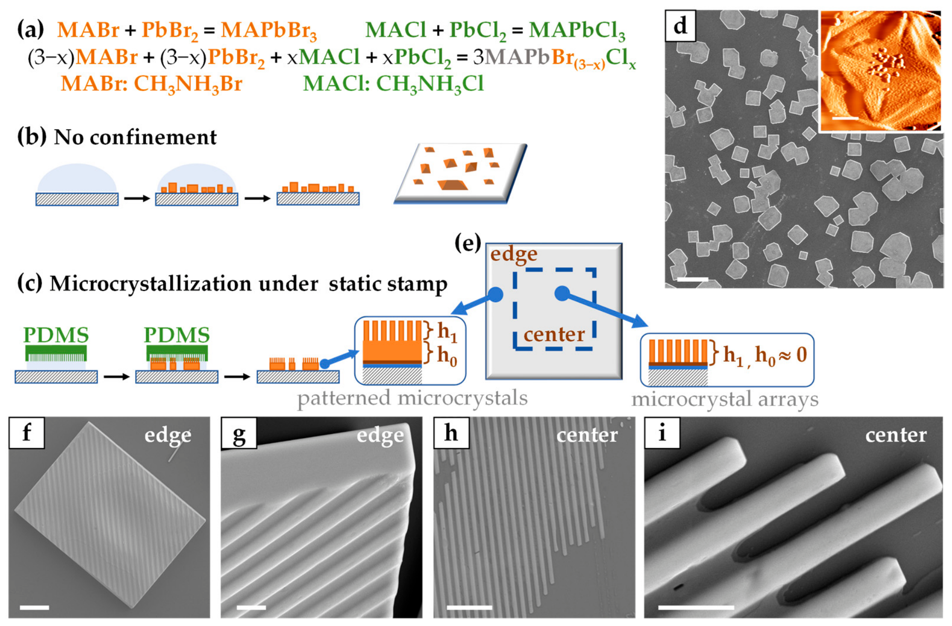
As a result, static PDMS-confined crystallization generates a broad range of microstructures on the same substrate, including crystals with different thicknesses, lateral dimensions, and local morphologies (Figures S3 and S4). This diversity is useful for manually identifying suitable microstructures and for exploratory studies aimed at recognizing representative growth modes and obtaining initial insight into patterned multicomponent crystallization. However, it also means that a single global statistical distribution of all crystallites on a substrate would not necessarily be physically meaningful, because the sampled objects may originate from different local growth regimes. Therefore, in this work, we rely on semi-quantitative analysis of selected representative structures to identify the most prominent morphological features and likely trends. From the wide variety of observed structures, the discussion primarily focuses on patterned microcrystals and microcrystal arrays (Figure 2c,e–i). The central zone, which is normally populated by microarrays, is usually ~500 µm × 500 µm. Although previous studies [20], perfect shape (Figure 2f), and selected supplementary analyses (Section 3.3) suggest that at least some of the observed microstructures may be single-crystalline, we use the terms “patterned microcrystals” and “microcrystal arrays” here without implying single-crystalline or polycrystalline nature unless supported by specific characterization.
To reduce the number of experimental variables, unless explicitly specified, experiments in this study were performed using a fixed pressure of ~8 kPa, a fixed crystallization temperature of 60 °C, and a fixed total precursor concentration of 1 M (Figure 2a). These conditions were chosen to provide a common baseline for comparing the effects of confinement, substrate, pattern geometry, and precursor composition without introducing additional changes in supersaturation, solvent evaporation rate, or overall precursor availability. We also primarily used a direct one-step crystallization method, in which the precursor solution was confined between the patterned PDMS stamp and the target substrate from the beginning of the experiment. An alternative two-step strategy, in which non-patterned flat microcrystals are first grown on the substrate and subsequently patterned by a second confined growth step using a patterned PDMS stamp, is attractive for generating patterned microcrystals rather than sparse arrays. However, this route introduces additional variables, including the morphology, thickness, orientation, surface quality, and partial dissolution or regrowth behavior of the pre-formed crystals. These factors make the resulting structures more difficult to interpret mechanistically.

3.2. Confined Growth and Morphological Control of Patterned MAPbBr3

We first examined the confined crystallization of MAPbBr3 as a reference system because this composition has been widely used in previous studies of PDMS-assisted perovskite microcrystallization and provides a suitable baseline for evaluating our patterned growth strategy. In the absence of PDMS confinement, spin-coating and thermal crystallization of the MAPbBr3 precursor solution produced randomly distributed faceted microcrystals with non-flat top surfaces (Figure 2b,d). The surface distribution of such crystals was reasonably uniform over the mm scale (Figure S5). These results are consistent with heterogeneous nucleation, unconfined growth, and uniform solvent evaporation across the whole solution–air interface. By contrast, when the precursor solution was confined between the substrate and a patterned PDMS stamp, the crystal morphology was strongly influenced by the imposed spatial confinement and by the local PDMS–substrate contact conditions. The one-step confined crystallization route yielded patterned MAPbBr3 microstructures whose morphology varied broadly across the confined region (Figure S3c and Figure 2f–i). Near the edge of the PDMS contact area, relatively thick patterned microcrystals (Figure 2e–g) often merged into large coalescent crystalline domains (Figure S3), whereas the central region more commonly contained isolated microrods or microcrystal arrays with negligible base thickness (h0 ≈ 0) (Figure 2e,h,i). This edge-to-center divergence indicates that static PDMS-confined crystallization does not simply replicate the template geometry uniformly across the substrate. Instead, it couples template-directed growth with local variations in precursor supply, solvent evaporation, mass transport, and mechanical confinement.
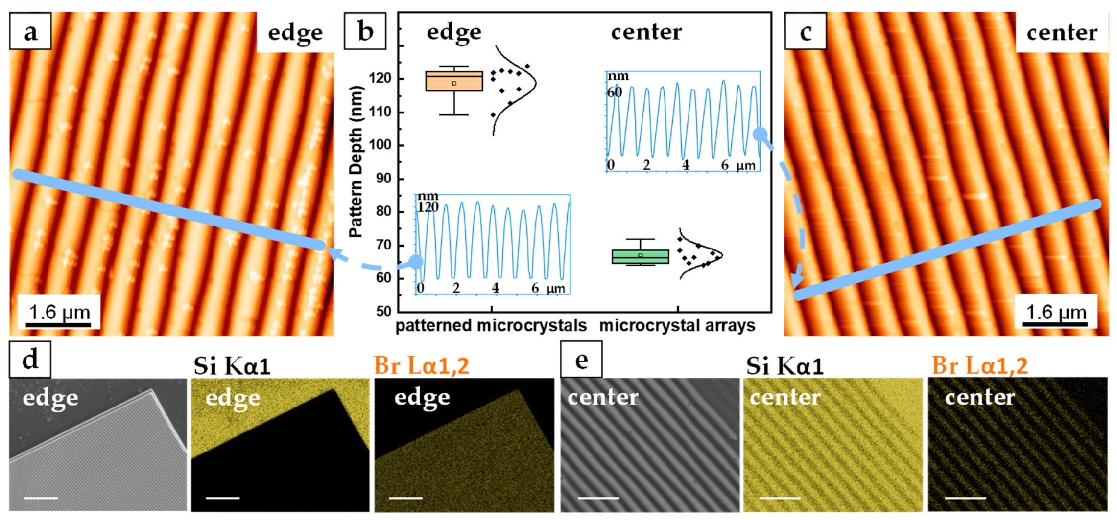
The morphology and composition of the two characteristic MAPbBr3 growth regimes were further examined by XRD, AFM, SEM, and EDX analysis. The XRD pattern of one-step patterned MAPbBr3 microcrystals grown on quartz shows only diffraction peaks assignable to the MAPbBr3 phase, with dominant (100), (200), and (300) reflections (Figure S6). This indicates phase-selective crystallization under the present conditions and suggests a strong preferential out-of-plane orientation of the microcrystals, with {100}-type planes predominantly aligned parallel to the substrate surface. AFM analysis of the 0.8 μm periodic structures further reveals a clear difference between the edge and center regions (Figure 3a–c). In the edge region, the patterned microcrystal exhibits a continuous grating morphology with a larger modulation depth, whereas the center region shows shallower, more isolated linear features. The pattern height in the edge region is approximately twice that measured in the central microcrystal arrays, confirming that the two regions represent distinct growth morphologies rather than only local variations in imaging contrast. Consistent with this interpretation, SEM and EDX mapping show that the edge structures consist of relatively thick patterned microcrystals with a continuous perovskite base layer and a superimposed linear grating (Figure 3d). In contrast, the central region is composed of isolated microrod arrays with negligible or very small base-layer thickness (h0 ≈ 0). In these central arrays, the underlying Si substrate can be detected between the perovskite microrods by Si Kα1 EDX mapping, further confirming h0 ≈ 0 (Figure 3e). It should be noted that, due to the nature of static stamp-confined microcrystallization, the height and thickness of the patterned features generally increase from the center of the confined region toward the edges. This radial variation is presumably associated with outward mass transport and enhanced precursor accumulation near the periphery during solvent evaporation. For example, even within a single sample, the thickness of the microcrystals can vary substantially over sub-millimeter distances (Figure S7). Therefore, exhaustive quantitative comparison of all structures is not practical or physically meaningful. Instead, we use semi-quantitative analysis to identify the main morphological trends.
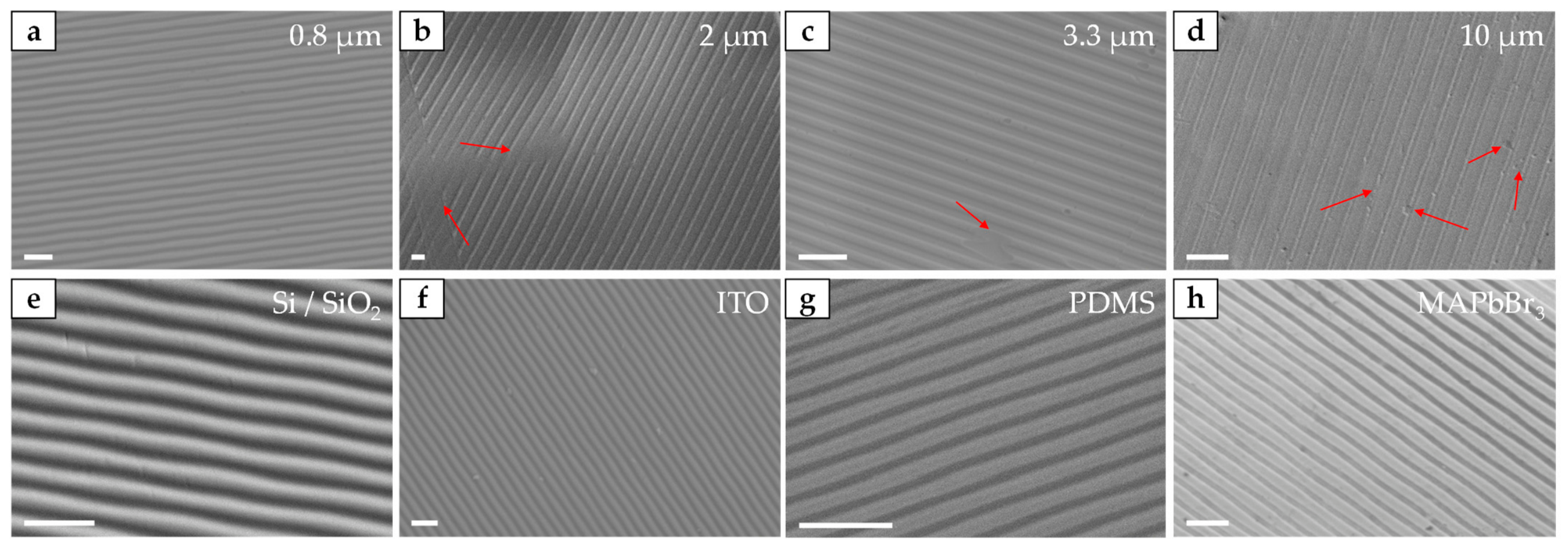
The generality of the patterned MAPbBr3 growth was further evaluated by varying both the template periodicity and the supporting substrate. Using PDMS stamps with different grating dimensions, periodic MAPbBr3 microstructures could be obtained with characteristic spacings of 0.8, 2, 3.3, and 10 μm (Figure 4a–d). In addition, patterned MAPbBr3 microcrystals were successfully formed on several different substrates (Figure 4e–h and Figure S8), including macroscopic MAPbBr3 single crystals, hereafter referred to as MAPbBr3 macrocrystals for brevity (Figure 4e–h). Growth on Si/SiO2 and ITO demonstrates compatibility with rigid oxide and conductive substrates relevant for optical and device characterization, whereas growth on PDMS indicates that the method can also be applied to flexible polymeric supports. The use of MAPbBr3 macrocrystals as substrates represents a distinct case because the substrate is chemically identical to the target material and may participate in interfacial growth or partial dissolution–recrystallization processes. Overall, these results show that static patterned PDMS confinement provides a convenient route to MAPbBr3 patterned microstructures with tunable periodicity and broad substrate compatibility.
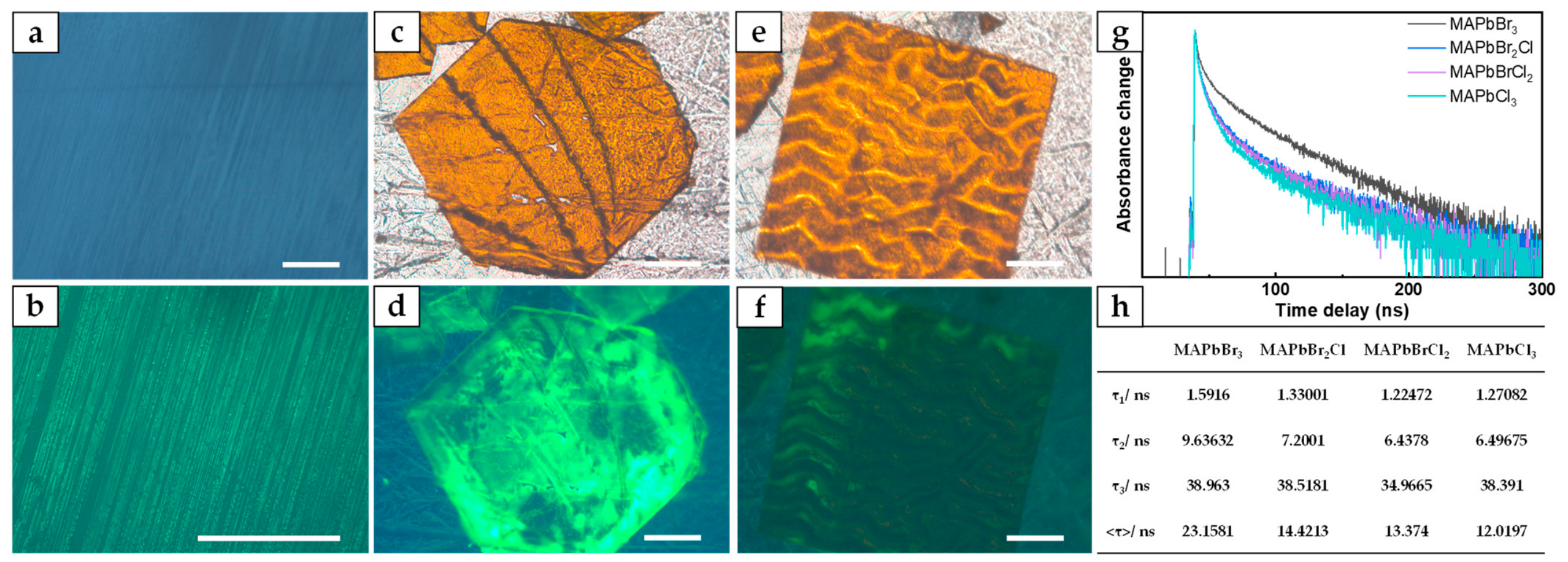
Fluorescence microscopy under 405 nm excitation further confirms that both isolated MAPbBr3 microcrystal arrays and larger patterned microcrystals are optically active (Figure 5a–f). The central microcrystal arrays exhibit spatially patterned green emission that follows the linear morphology of the confined structures, supporting their assignment as discrete emissive MAPbBr3 features rather than only residual surface topography (Figure 5a,b). Larger patterned microcrystals also show intense green emission across the crystal area, although the emission intensity is spatially non-uniform (Figure 5c,d). Because MAPbBr3 is a single-halide reference composition, these intensity variations are more reasonably attributed to local differences in crystal thickness, surface morphology, optical outcoupling, and defect-assisted non-radiative recombination, rather than to compositional variation. Similarly, wrinkled structures remain emissive and display green PL characteristic of MAPbBr3, indicating that wrinkle formation does not necessarily correspond to a distinct non-emissive phase or complete degradation of the perovskite (Figure 5e,f). Overall, PL microscopy provides qualitative confirmation of emissive perovskite formation in the different morphological regimes while also illustrating that local topography and morphology strongly influence the observed emission intensity.
Time-resolved photoluminescence (TRPL) measurements were performed to compare the effective recombination dynamics of the MAPbBr3−xClx patterned microstructures as a function of nominal halide composition (Figure 5g,h). The decay curves could not be adequately described by a simple biexponential model and were therefore fitted using a tri-exponential function, yielding three characteristic decay components, τ1, τ2, and τ3, together with an average lifetime, ⟨τ⟩. The need for three exponential components should be interpreted phenomenologically: it indicates that the measured emission arises from a heterogeneous ensemble of recombination environments rather than from a single uniform crystalline population. This is consistent with the morphology of the statically confined samples, which contain exposed surfaces, edges, variable thicknesses, possible domain boundaries, and locally different crystallization quality. For this reason, the TRPL discussion is presented as a comparative analysis across the MAPbBr3−xClx series rather than as an intrinsic lifetime analysis of individual homogeneous microcrystals.
Within this comparative framework, the MAPbBr3 reference sample shows the longest average lifetime, ⟨τ⟩ = 23.16 ns, whereas the mixed-halide and chloride-rich samples exhibit shorter average lifetimes of 14.42 ns for MAPbBr2Cl, 13.37 ns for MAPbBrCl2, and 12.02 ns for MAPbCl3. The fast and intermediate decay components also decrease slightly upon Cl incorporation, suggesting a greater contribution from surface-, defect-, or interface-assisted nonradiative recombination pathways in the mixed-halide and chloride-rich microstructures. In contrast, the slow component remains in a similar range across the series, indicating that longer-lived recombination channels are still present but contribute differently to the overall decay. Overall, the TRPL data show that halide composition and mixed-halide crystallization affect the effective recombination dynamics of the patterned microstructure ensembles. However, because the measurements average over morphologically heterogeneous regions, the results should be used primarily for comparative assessment across the nominal compositions, rather than as direct evidence of single-crystal quality, homogeneous composition, or uniquely assignable recombination mechanisms.

3.3. Typical Structural Defects and Imperfections in Patterned Perovskite Microcrystals

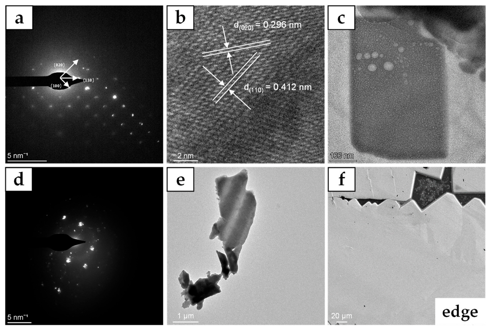
As discussed above, XRD measurements indicate the formation of the MAPbBr3 phase under the selected crystallization conditions at 60 °C. Local TEM analysis further shows that at least some patterned microstructures are single-crystalline or highly single-crystal-like. In one representative region (Figure 6a–c), the selected-area electron diffraction (SAED) pattern displays sharp and discrete diffraction spots without obvious diffraction rings, while the corresponding HRTEM image shows continuous lattice fringes with measured spacings of d(200) ≈ 0.296 nm and d(110) ≈ 0.412 nm, consistent with crystalline MAPbBr3 (Figure 6b). These observations demonstrate that patterned PDMS confinement can generate well-crystallized MAPbBr3 domains under the present conditions.
However, this single-crystalline character should not be generalized to all patterned microstructures obtained in the same experiment. Because nucleation is not spatially predefined in the static PDMS-stamping method, neighboring nuclei can form close to each other and grow simultaneously within the confined precursor film. When such domains laterally impinge, they may coalesce into larger aggregates even if their crystallographic orientations are not identical. This behavior is illustrated by the second TEM region, where the SAED pattern contains multiple sets of diffraction spots, indicating contributions from differently oriented crystalline domains rather than a single coherent crystal (Figure 6d,e). Similar behavior is frequently observed in edge regions, where increased precursor supply and stronger growth can produce laterally merged domains. In SEM images, these edge structures often show visible domain boundaries and irregular coalesced crystal arrangements, consistent with locally polycrystalline or multidomain growth (Figure 6f).
These observations highlight an intrinsic limitation of the selected crystallization strategy. Static PDMS stamping is experimentally simple and effective for transferring patterns, but it does not guide nucleation with the precision provided by lithographically defined nucleation sites, hydrophilic/hydrophobic templates, or patterned homoepitaxial growth. Therefore, coalescence of independently nucleated domains and formation of multidomain or polycrystalline aggregates are statistically unavoidable, especially in regions where nucleation density or precursor availability is high. For individual microdevice fabrication, researchers can manually select crystals with a suitable size and morphology and then verify their crystallographic quality by local methods such as SAED, EBSD, or micro-XRD. However, performing such confirmations for every microstructure across an entire sample would be expensive, time-consuming, and impractical. For this reason, the present work focuses primarily on pattern transfer, morphology, and practical growth behavior, rather than assigning a single-crystal or polycrystalline nature to every observed structure. When uniform size, controlled nucleation, and guaranteed single-crystal character across large areas are required, more deterministic patterning or epitaxial crystallization approaches, such as those discussed in Section 3.1, should be considered. It is also useful to mention, as a recurring type of morphological imperfection, the periodically observed nanoscale crystallites on the patterned microstructures (Figure 3a and Figure S9b). At present, it is unclear whether these particles originate from sedimentation of small crystallites formed in solution or from secondary nucleation and growth on the surface of the perovskite microstructures. The latter explanation appears more plausible because the particles are often arranged in lines along the upper regions of the perovskite gratings. However, their origin, formation mechanism, size uniformity, and apparent spatial ordering remain unresolved. Future studies will be required to clarify their origin and assess their potential applications as hierarchical self-organized structures.
Pattern-transfer imperfections were also observed and can be attributed to both the PDMS template and the local substrate/contact conditions. In several patterned MAPbBr3 microstructures, local disruptions, missing stripe segments, or irregular line distortions appear at positions consistent with defects or contamination on the PDMS stamp itself (Figure 4b–d, red arrows). Such features are transferred together with the intended grating morphology and therefore represent practical limitations of using soft, reusable PDMS templates. In addition, even when the stamp pattern is well defined, incomplete or non-uniform transfer can occur because the PDMS stamp does not always maintain perfectly conformal contact with the substrate during crystallization. This effect is especially important on rough, defective, or polycrystalline perovskite surfaces, where pre-existing topography can locally prevent uniform confinement. For example, patterned growth on a polycrystalline MAPbBr3 film supported by PDMS produced only partially transferred 2 μm features, while growth on a defective region of a MAPbBr3 macrocrystal yielded incomplete 0.8 μm patterning (Figure S10). These observations indicate that pattern fidelity is governed not only by the nominal stamp periodicity, but also by stamp quality, local contact pressure, substrate flatness, and the presence of pre-existing surface defects. Therefore, although static PDMS stamping provides a simple route to patterned perovskite microcrystals, improved control over template cleanliness, stamp deformation, substrate planarity, and conformal contact would be required for more uniform pattern replication. More advanced nanoimprint or controlled-contact strategies may help mitigate these limitations when high-fidelity large-area patterning is required.
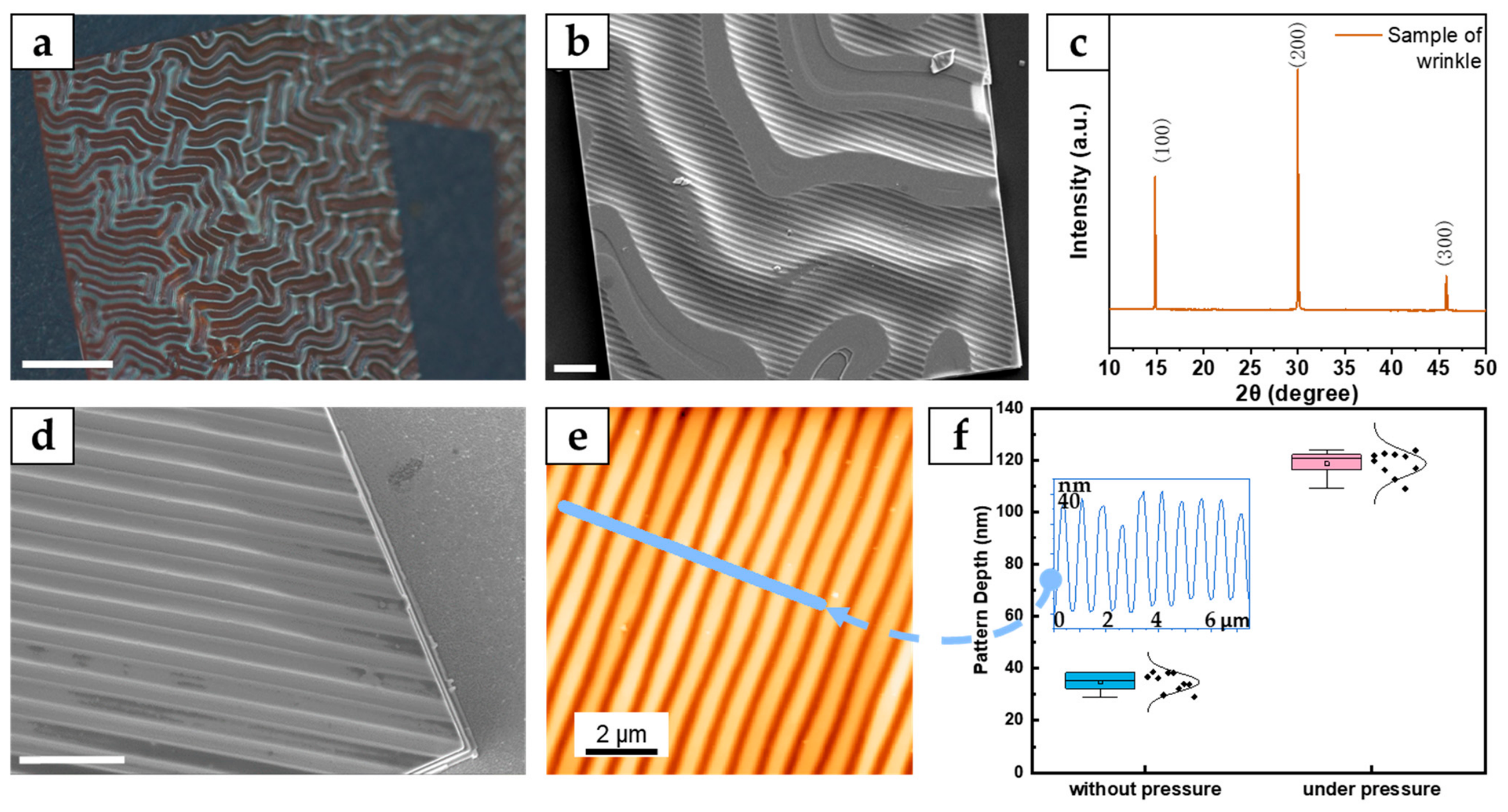
Previously unreported wrinkled morphologies were also frequently observed in patterned MAPbBr3 microcrystals grown under the confinement of static PDMS stamps (Figure 5e, Figure 7a and Figure S11). Optical and fluorescence microscopy (Figure 5e,f and Figure S11a,b) show that these wrinkled regions retain the characteristic green emission of MAPbBr3 under 405 nm excitation, indicating that the corrugated areas remain optically active perovskite rather than non-emissive residues or fully degraded material. XRD analysis (Figure 7c) further confirms that the wrinkled samples are still composed of the MAPbBr3 phase and exhibit strong preferential orientation with respect to the substrate surface. SEM imaging reveals that the wrinkles correspond to surface morphological corrugations superimposed on otherwise linearly patterned microcrystals (Figure S11c,d). In some cases, the crystal top surface is flat with the intended linear grating pattern clearly visible in the regions between the wrinkles (Figure 7b).
The origin of these wrinkles is most likely mechanical rather than compositional. Similar stress-induced distortions are known in soft-template or confined-growth systems [27], and in the present case they may arise from the combined effects of PDMS elasticity, compressive loading, and well-known swelling of PDMS in organic solvents. This interpretation is supported by inspection of the PDMS stamp after crystallization under an applied pressure of approximately 8 kPa, which revealed clearly visible wrinkle-like features on the PDMS surface itself (Figure S12a). To separate the roles of solvent exposure and mechanical pressure, control experiments were performed without applying additional external pressure. When the PDMS stamp was simply placed on top of the substrate, wrinkle-free patterned MAPbBr3 crystallization was obtained, although the pattern depth was lower than in pressure-assisted experiments (Figure 7d–f). In addition, heating the PDMS template at 60 °C in the presence of DMSO but without applied pressure did not generate comparable wrinkles (Figure S12b). These observations suggest that solvent exposure alone is insufficient to produce the observed deformation under the tested conditions, whereas applied pressure is a key factor promoting wrinkling of the PDMS stamp and its subsequent transfer to the growing perovskite microcrystals. Consequently, pressure improves conformal contact and pattern depth, but excessive or poorly controlled loading can also introduce stamp deformation and secondary wrinkle patterns.

3.4. Patterned Crystallization of MAPbBr3−xClx

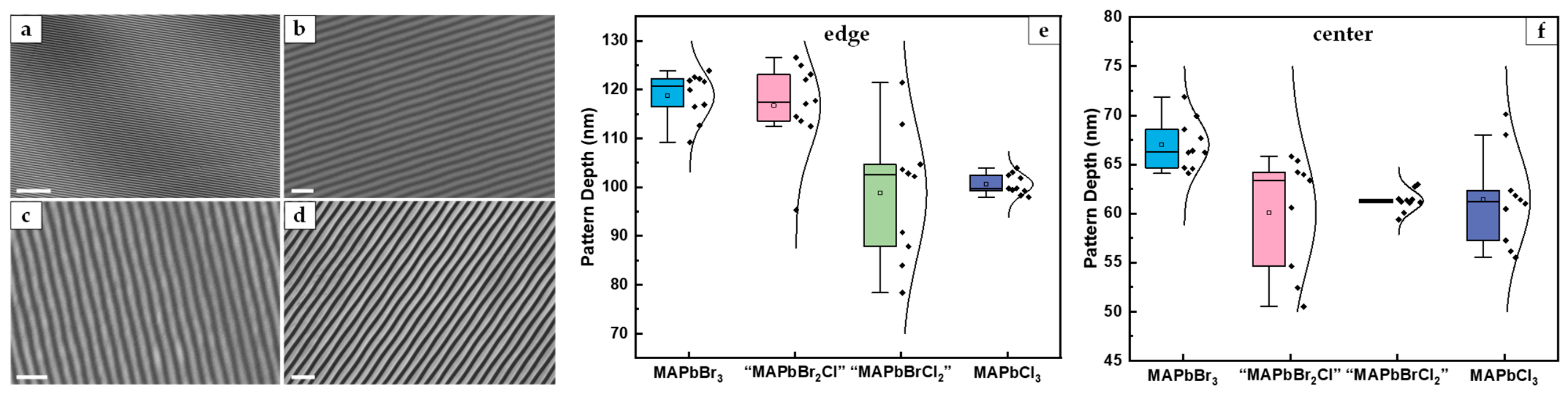
The template-assisted confined crystallization strategy was next extended from the single-halide MAPbBr3 reference system to the mixed-halide MAPbBr3−xClx system. For these experiments, a 1 M DMF solution of MAPbBr3 and a 1 M DMSO solution of MAPbCl3 were mixed according to the desired nominal Br/Cl precursor ratio and crystallized under otherwise identical static PDMS-confined conditions. Patterned microstructures were successfully obtained for all investigated nominal compositions (Figure 8a–d and Figure S13), including MAPbBr3, MAPbBr2Cl, MAPbBrCl2, and MAPbCl3. The resulting morphologies were broadly similar to those observed for the MAPbBr3 reference system: the pattern depths of microcrystals formed at the sample edge (Figure 8e) were consistently larger than those of microarrays formed at the center (Figure 8f).
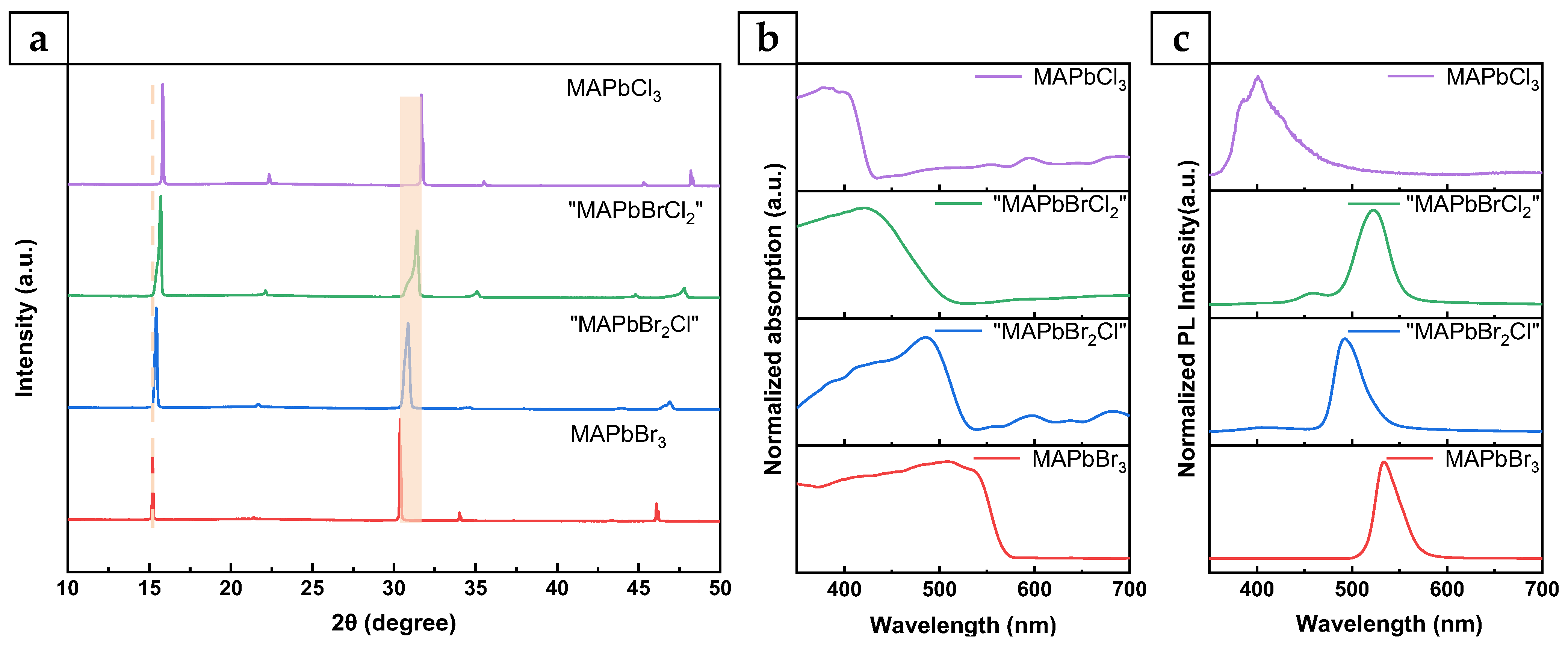
XRD, UV–Vis absorption, photoluminescence, and EDX measurements all confirm that changing the nominal Br/Cl precursor ratio leads to composition-dependent structural and optical changes in the confined MAPbBr3−xClx microcrystals (Figure 9 and Figures S14–S20). In the XRD patterns, the main diffraction peaks shift systematically with increasing nominal Cl content, consistent with partial substitution of Br by the smaller Cl ion and the corresponding contraction of the perovskite lattice. The absorption edge and PL emission also shift with precursor composition, confirming that the halide composition influences the optical bandgap of the resulting microcrystals. However, when plotted against nominal solution (Figure S21a,b) or EDX determined Cl/(Cl + Br) on-surface compositions (Figure S21c,d), the evolutions are not strictly linear (Figure S21), and the deviation is particularly evident for the “MAPbBrCl2” sample. This sample has a highly asymmetric (200) peak, a shallow absorption shoulder, and a very strong additional luminescence peak at a wavelength longer than expected (Figure 9). Additional PL and XRD experiments with MAPbBr1.5Cl1.5 and MAPbBr0.5Cl2.5 confirmed that they also exhibit anomalous behavior similar to that of MAPbBrCl2 (Figure S22). In the present system, further interpretation is complicated because changing the nominal halide composition also changes the solvent composition: MAPbBr3 was prepared from a DMF solution, whereas MAPbCl3 was prepared from a DMSO solution. Therefore, variation in the Br/Cl ratio is coupled to variation in DMF/DMSO ratio, which can affect precursor coordination, solubility, evaporation behavior, supersaturation, and crystallization kinetics.
To eliminate solvent-induced confounding effects, the MAPbBr3−xClx compositional series was repeated using DMSO as the sole solvent for all precursor solutions. DMSO was selected because chloride-rich lead halide perovskite precursors are generally less soluble in pure DMF, making a single-solvent DMF series impractical. The number of nominal Br/Cl ratios was increased to seven, and the resulting morphology was examined by SEM at four edge positions and one central position for each composition (Figure S4). Across the entire DMSO-based series, the characteristic spatial divergence observed for the MAPbBr3 reference system was reproduced: dense, laterally extended patterned microcrystals formed predominantly near the edge region, whereas the central region contained more isolated and sparse patterned arrays. Thus, the edge–center morphology contrast is not specific to the mixed DMF/DMSO system, but appears to be an intrinsic feature of static PDMS-confined crystallization.
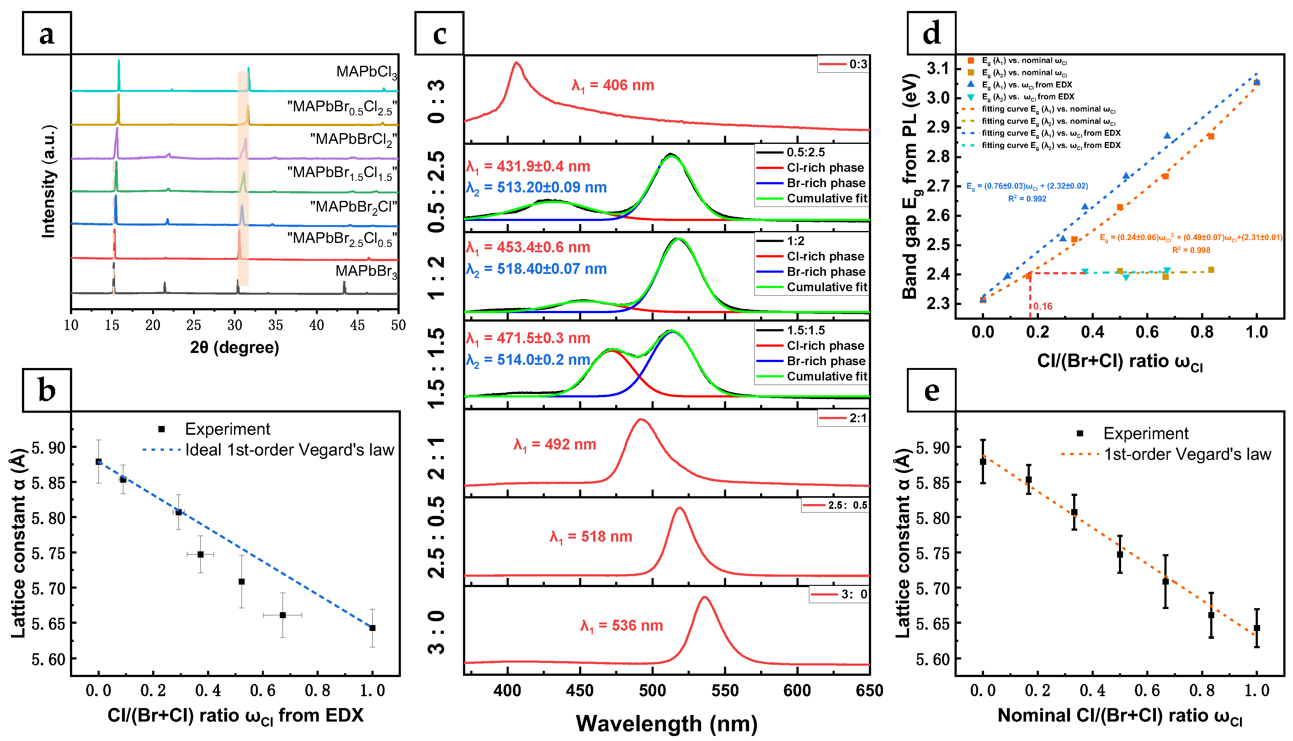
XRD analysis of the DMSO-based series showed systematic composition-dependent shifts in the perovskite diffraction peaks (Figure 10a), confirming that the halide composition of the patterned microstructures can be tuned. However, plotting the lattice constant against the EDX-determined surface composition, ωCl = Cl/(Cl + Br), revealed clear deviation from ideal first-order Vegard behavior for mixed compositions with ωCl > 0.3 (Figure 10b). In contrast, replotting the lattice constant as a function of nominal solution composition gave an apparently good linear fit (Figure 10e). This indicates that the precursor formulation reproducibly controls the structural evolution of the crystallized material, but that the EDX-measured surface composition and the XRD-derived lattice response are not fully described by a simple homogeneous solid-solution model.
Photoluminescence measurements further support this conclusion. For Cl-rich nominal compositions, a second strong emission band near 514 nm was observed (Figure 10c). Broadening around this wavelength already appears at the nominal 2:1 Br:Cl ratio, and the spectra of the 1.5:1.5, 1:2, and 0.5:2.5 samples can be deconvoluted into two distinct emission components. The shorter-wavelength component follows the expected blue-shift with increasing Cl content, while the nearly fixed emission near 514 nm suggests the presence of an additional low-bandgap emissive environment. Because the XRD patterns do not show obvious reflections outside the MAPbBr3−xClx perovskite family, this low-bandgap emission is most plausibly assigned to a Br-rich MAPbBr3−xClx domain rather than to a separate non-perovskite impurity phase. Using a Vegard-type estimate, this emissive Br-rich component corresponds approximately to MAPbBr2.52Cl0.48, although this value should be treated as an effective composition rather than an exact stoichiometry (Figure 10d).
Two possible interpretations can be considered for this nearly constant Br-rich emission. The first is that MAPbBr2.52Cl0.48 represents an approximate solubility or saturation limit for Cl incorporation into a Br-rich phase under the present crystallization conditions. If this were the dominant explanation, preferential formation of this Br-rich phase would be expected to consume Br from the local solution, leaving a more Cl-rich residual solution from which a second, Cl-rich phase would crystallize. In that case, the composition of the Cl-rich component might be expected to deviate strongly from the nominal precursor ratio. However, the shorter-wavelength PL component and the lattice constants plotted against nominal precursor composition both show comparatively regular composition-dependent trends. This behavior is not easily reconciled with a simple equilibrium two-phase model defined by two fixed terminal compositions.
A second, more plausible interpretation is that the near-514 nm emission arises from a kinetically favored Br-rich nucleation product. In this scenario, nuclei with an approximate MAPbBr2.52Cl0.48-like composition form rapidly at the early stage of crystallization, after which further growth proceeds more nearly according to the remaining local solution composition. This would explain why one emission component remains nearly fixed, while the other shifts systematically with the nominal Br/Cl ratio. Additional indirect support for this interpretation comes from PL microscopy of selected Cl-rich mixed-halide microstructures, where no isolated bright green emission spots characteristic of exposed MAPbBr2.52Cl0.48-like domains were observed; instead, only pale blue emission associated with Cl-rich perovskite regions was visible (Figure S23). This suggests that the Br-rich emissive domains, if present, may be buried beneath or surrounded by more Cl-rich material. Under low-intensity wide-field PL microscopy, such buried domains may be insufficiently excited or optically screened, whereas the higher excitation intensity and collection geometry used in ensemble PL spectroscopy may still allow their contribution to appear as a strong green emission band.
Overall, the DMSO-only series demonstrates that static PDMS-confined crystallization enables systematic tuning of MAPbBr3−xClx patterned microstructures, but the resulting materials do not behave as a single ideal solid solution over the entire composition range. Instead, the combined XRD, EDX, and PL data indicate compositionally heterogeneous crystallization, particularly in Cl-rich precursor formulations. The most consistent interpretation is that a Br-rich emissive component forms preferentially during early nucleation, while subsequent growth produces a more Cl-rich perovskite phase more closely reflecting the composition of the remaining precursor solution.
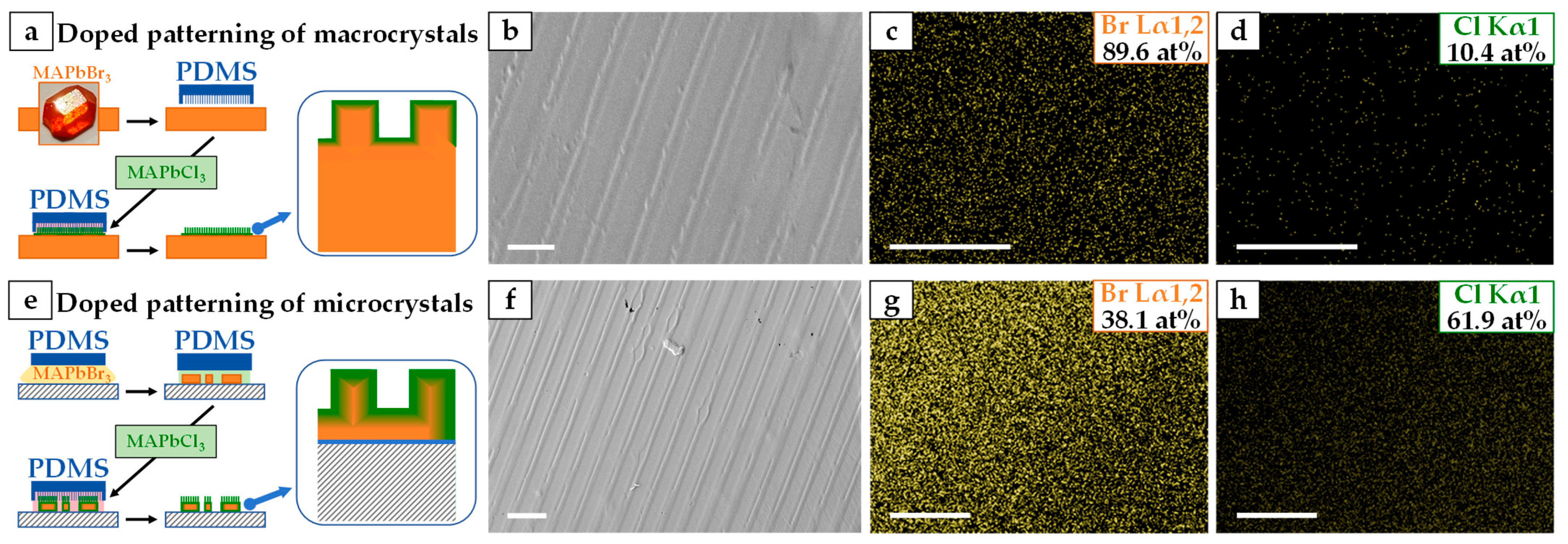
Finally, the patterned crystallization strategy was briefly extended to mixed-halide growth on pre-existing MAPbBr3 crystals. This experiment builds on the MAPbBr3-on-MAPbBr3 patterned growth shown in Figure 4h, but replaces the MAPbBr3 precursor with a 1 M MAPbCl3 solution confined under a patterned PDMS stamp at 60 °C (Figure 11a). When a flat MAPbBr3 macroscopic single crystal, hereafter referred to as a MAPbBr3 macrocrystal, was used as the substrate, a linearly patterned surface was obtained (Figure 11b). The 10 μm periodicity of the resulting pattern is comparable to that observed for MAPbBr3 crystallization on MAPbBr3 macrocrystals, confirming that the PDMS template can also direct surface patterning during heterohalide precursor exposure. EDX mapping shows that, in addition to the expected bromine signal from the MAPbBr3 substrate, chlorine is also clearly detected and is distributed across the patterned surface (Figure 11c,d). However, the absolute EDX values should be interpreted cautiously: at the 10 kV accelerating voltage used for imaging, the electron interaction depth in lead-halide perovskites can approach the micrometer scale, and the chloride diffusion depth or compositional gradient within the crystal is not known. Therefore, the EDX maps confirm chloride incorporation or surface enrichment, but do not allow a precise quantitative determination of the depth profile or local stoichiometry.
A similar experiment performed on flat MAPbBr3 microcrystals also produced the desired 10 μm linear patterning (Figure 11e,f). Under the same SEM–EDX conditions, however, the detected chlorine content was substantially higher than that in the MAPbBr3 macrocrystal substrate (Figure 11g,h). This difference is consistent with the much smaller bromide reservoir and higher surface-to-volume ratio of the microcrystals. During contact between the MAPbCl3/DMSO precursor solution and a MAPbBr3 crystal, several interfacial processes can occur simultaneously: partial dissolution of MAPbBr3, reprecipitation of mixed-halide MAPbBr3−xClx material, chloride/bromide exchange, and possible diffusion of chloride into the MAPbBr3 matrix. These processes are further coupled to PDMS microconfinement, local solvent evaporation, template-imposed mass transport, and dynamically changing concentration gradients. Because the available MAPbBr3 volume is limited in microcrystals, halide exchange or mixed-halide reprecipitation can proceed to a greater apparent extent than on macroscopic MAPbBr3 crystals. Thus, these preliminary experiments indicate that patterned PDMS confinement can be combined with substrate-mediated halide exchange or interfacial recrystallization, but a more detailed mechanistic analysis would require depth-resolved composition mapping and time-dependent studies.


4. Conclusions

In this work, static PDMS-template-confined crystallization was established as a simple exploratory platform for producing patterned MAPbBr3 and MAPbBr3−xClx perovskite microstructures. Using patterned PDMS stamps, periodic microcrystals and microcrystal arrays were obtained over different template periodicities and on several substrates, including Si/SiO2, ITO, PDMS, and MAPbBr3 macrocrystals. The MAPbBr3 reference system confirmed successful pattern transfer while also revealing important practical limitations of static stamping, including edge–center morphological divergence, stochastic nucleation, coalesced domains, incomplete pattern transfer, pressure-induced wrinkling, and secondary nanoscale crystallites. Extension to MAPbBr3−xClx showed that patterned mixed-halide microstructures can be obtained with composition-dependent structural and optical properties. However, XRD, EDX, PL, and TRPL analyses indicate that the system is not fully described by a simple homogeneous solid-solution model, particularly in Cl-rich compositions, where a Br-rich emissive component and compositionally heterogeneous crystallization are likely involved. Overall, the results clarify that static PDMS-confined crystallization is useful for generating diverse patterned perovskite microstructures and selecting individual crystals for further study, but it should not be regarded as a deterministic method for producing statistically uniform single-crystal arrays without further process control.
Future work should focus on resolving the local structure–composition–property relationships that remain inaccessible from surface-averaged measurements. In particular, cross-sectional elemental mapping will be important for determining whether mixed-halide compositions are laterally segregated, vertically graded, or core–shell-like. The nanoscale crystallites periodically observed on top of the perovskite gratings could also be investigated further because of their origin, optical properties, and possible applications. Finally, the static-stamp experiments reported here provide a practical foundation for moving toward dynamic confined crystallization systems, including microchannels of specially designed microfluidic chips, where precursor supply, solution composition, residence time, and local mass transport can be controlled more precisely.

Supplementary Materials

The following supporting information can be downloaded at: https://www.mdpi.com/article/10.3390/cryst16060361/s1. Figure S1: Structural and optical characterization confirming the quality of bulk MAPbBr3 single crystals, including XRD, absorption/Tauc analysis, PL, and TRPL measurements; Figure S2: Schematic and photographic illustrations of the ~8 kPa pressure-loading setup used for confined crystal growth; Figure S3: Morphological comparison between center and edge regions of patterned MAPbBr3 microcrystals grown under applied pressure on different substrates; Figure S4: SEM overview of MAPbBr3−xClx microstructures with various Br:Cl ratios grown in a DMSO-only system, highlighting morphology evolution between edge and center regions; Figure S5: Millimeter-scale spatial distribution of unconstrained MAPbBr3 polyhedral microcrystals without PDMS confinement; Figure S6: XRD pattern confirming the crystal structure of one-step patterned MAPbBr3 microcrystals grown under ~8 kPa pressure; Figure S7: Thickness distribution and corresponding tilted-view SEM images of distributed MAPbBr3 microcrystals; Figure S8: Low-magnification SEM comparison of MAPbBr3 patterned microcrystals grown on PDMS, silicon wafer, ITO, and a MAPbBr3 single-crystal substrates; Figure S9: AFM characterization and cross-sectional profiles of patterned MAPbBr3−xClx microcrystal arrays with different halide compositions; Figure S10: Incomplete patterned growth directly formed on defective or polycrystalline perovskite substrates under applied pressure; Figure S11: Optical, fluorescence, and SEM characterization of wrinkle-like patterned MAPbBr3 structures grown on PDMS substrates; Figure S12: Optical microscopy characterization of PDMS templates before and after wrinkle formation and DMSO treatment; Figure S13: Top and tilted view SEM morphology of patterned MAPbBr3−xClx microstructures with different halide compositions; Figure S14: Line-scan EDX analysis comparing elemental distributions in isolated MAPbBr2Cl microcrystal arrays and continuous patterned microcrystals; Figures S15–S18: Top-view planar EDX maps confirming uniform elemental distribution (no lateral segregation) in patterned microcrystals of MAPbBr3, MAPbBr2Cl, MAPbBrCl2, and MAPbCl3; Figures S19 and S20: Top-view planar EDX maps demonstrating uniform elemental distribution specifically within isolated microcrystal arrays (where the substrate is exposed between stripes) for MAPbBrCl2 and MAPbCl3; Figure S21: Composition-dependent evolution of lattice constant and optical bandgap for confined-grown MAPbBr3−xClx microcrystals in a DMF:DMSO mixed-solvent system; Figure S22: Additional XRD and PL characterization of MAPbBr0.5Cl2.5 and MAPbBr1.5Cl1.5 microcrystals grown in a DMF:DMSO mixed-solvent system; Figure S23: Optical and fluorescence microscopy images of patterned MAPbBr3−xClx microcrystals with different mixed-halide compositions in a DMSO-only system.

Author Contributions

Conceptualization, Y.F. and O.I.; methodology, J.W. and P.Z.; validation, J.W. and P.Z.; formal analysis, J.W.; investigation, J.W., P.Z., Z.W. and Y.Z.; resources, Y.F. and O.I.; data curation, J.W. and P.Z.; writing—original draft preparation, J.W. and O.I.; writing—review and editing, J.W., P.Z., Y.F. and O.I.; supervision, Y.F. and O.I.; funding acquisition, Y.F. and O.I. All authors have read and agreed to the published version of the manuscript.

Funding

This research was funded by the National Natural Science Foundation of China (Grant Nos. 22372110, 22372111, 22350610244, U24A20496, and 22161132026), the Suzhou Key Laboratory of Surface and Interface Intelligent Matter (Grant No. SZS2022011), the Gusu Innovation and Entrepreneurship Talent Program–Major Innovation Team (Grant No. ZXD2023002), the Center for Innovation in the Molecular Science of Surface and Interface (CIMSSI), the Suzhou Key Laboratory of Functional Nano & Soft Materials, the Collaborative Innovation Center of Suzhou Nano Science & Technology, and the 111 Project.

Data Availability Statement

The data presented in this study are available on request from the corresponding author.

Acknowledgments

During the preparation of this manuscript, the authors used ChatGPT Plus 5.2 for the purposes of improving the coherence and style of manuscript text. The authors have reviewed and edited the output and take full responsibility for the content of this publication.

Conflicts of Interest

The authors declare no conflicts of interest.

Abbreviations

The following abbreviations are used in this manuscript:
MAMethylammonium
NILNanoimprint lithography
PDMSPolydimethylsiloxane
ITOIndium tin oxide
XRDX-ray diffraction
EDXEnergy-dispersive X-ray
DVDDigital versatile disc
SEMScanning electron microscopy
AFMAtomic force microscopy
TEMTransmission electron microscope
SAEDSelected area electron diffraction
EBSDElectron backscatter diffraction
TRPLTime-resolved photoluminescence

References

  1. Fang, Y.; Dong, Q.; Shao, Y.; Yuan, Y.; Huang, J. Highly Narrowband Perovskite Single-Crystal Photodetectors Enabled by Surface-Charge Recombination. Nat. Photon 2015, 9, 679–686. [Google Scholar] [CrossRef]
  2. Khoram, P.; Brittman, S.; Dzik, W.I.; Reek, J.N.H.; Garnett, E.C. Growth and Characterization of PDMS-Stamped Halide Perovskite Single Microcrystals. J. Phys. Chem. C 2016, 120, 6475–6481. [Google Scholar] [CrossRef]
  3. Wang, X.; Li, Y.; Xu, Y.; Pan, Y.; Zhu, C.; Zhu, D.; Wu, Y.; Li, G.; Zhang, Q.; Li, Q.; et al. Solution-Processed Halide Perovskite Single Crystals with Intrinsic Compositional Gradients for X-Ray Detection. Chem. Mater. 2020, 32, 4973–4983. [Google Scholar] [CrossRef]
  4. Li, S.; Xia, H.; Wang, L.; Sun, X.; An, Y.; Zhu, H.; Bai, B.; Sun, H. Self-Powered and Flexible Photodetector with High Polarization Sensitivity Based on MAPbBr3–MAPbI3 Microwire Lateral Heterojunction. Adv. Funct. Mater. 2022, 32, 2206999. [Google Scholar] [CrossRef]
  5. Liu, Y.; Yang, Z.; Cui, D.; Ren, X.; Sun, J.; Liu, X.; Zhang, J.; Wei, Q.; Fan, H.; Yu, F.; et al. Two-Inch-Sized Perovskite CH3NH3PbX3 (X = Cl, Br, I) Crystals: Growth and Characterization. Adv. Mater. 2015, 27, 5176–5183. [Google Scholar] [CrossRef]
  6. Dong, Q.; Fang, Y.; Shao, Y.; Mulligan, P.; Qiu, J.; Cao, L.; Huang, J. Electron-hole Diffusion Lengths > 175 μm in Solution-Grown CH3NH3PbI3 Single Crystals. Science 2015, 347, 967–970. [Google Scholar] [CrossRef] [PubMed]
  7. Lei, Y.; Chen, Y.; Gu, Y.; Wang, C.; Huang, Z.; Qian, H.; Nie, J.; Hollett, G.; Choi, W.; Yu, Y.; et al. Controlled Homoepitaxial Growth of Hybrid Perovskites. Adv. Mater. 2018, 30, 1705992. [Google Scholar] [CrossRef]
  8. Wei, H.; DeSantis, D.; Wei, W.; Deng, Y.; Guo, D.; Savenije, T.J.; Cao, L.; Huang, J. Dopant Compensation in Alloyed CH3NH3PbBr3−xClx Perovskite Single Crystals for Gamma-Ray Spectroscopy. Nat. Mater. 2017, 16, 826–833. [Google Scholar] [CrossRef] [PubMed]
  9. Islam, M.J.; Yuyama, K.; Takahashi, K.; Nakamura, T.; Konishi, K.; Biju, V. Mixed-Halide Perovskite Synthesis by Chemical Reaction and Crystal Nucleation Under an Optical Potential. NPG Asia Mater. 2019, 11, 31. [Google Scholar] [CrossRef]
  10. Abe, R.; Suzuki, A.; Watanabe, K.; Kikuchi, A. Fabrication of CH3NH3PbBr3-Based Perovskite Single-Crystal Arrays by Spin-Coating Method Using Hydrophobic Patterned Substrate. Phys. Status Solidi (A) 2020, 217, 1900511. [Google Scholar] [CrossRef]
  11. Xu, Z.; Han, X.; Wu, W.; Li, F.; Wang, R.; Lu, H.; Lu, Q.; Ge, B.; Cheng, N.; Li, X.; et al. Controlled on-Chip Fabrication of Large-Scale Perovskite Single Crystal Arrays for High-Performance Laser and Photodetector Integration. Light Sci. Appl. 2023, 12, 67. [Google Scholar] [CrossRef]
  12. Cloutier, S.G.; Kossyrev, P.A.; Xu, J. Optical Gain and Stimulated Emission in Periodic Nanopatterned Crystalline Silicon. Nat. Mater. 2005, 4, 887–891. [Google Scholar] [CrossRef]
  13. Chen, W.; Tymchenko, M.; Gopalan, P.; Ye, X.; Wu, Y.; Zhang, M.; Murray, C.B.; Alu, A.; Kagan, C.R. Large-Area Nanoimprinted Colloidal Au Nanocrystal-Based Nanoantennas for Ultrathin Polarizing Plasmonic Metasurfaces. Nano Lett. 2015, 15, 5254–5260. [Google Scholar] [CrossRef] [PubMed]
  14. Park, J.; Kyhm, J.; Kim, H.; Jeong, S.; Kang, J.; Lee, S.; Lee, K.; Park, K.; Barange, N.; Han, J.; et al. Alternative Patterning Process for Realization of Large-Area, Full-Color, Active Quantum Dot Display. Nano Lett. 2016, 16, 6946–6953. [Google Scholar] [CrossRef] [PubMed]
  15. Wang, H.; Haroldson, R.; Balachandran, B.; Zakhidov, A.; Sohal, S.; Chan, J.Y.; Zakhidov, A.; Hu, W. Nanoimprinted Perovskite Nanograting Photodetector with Improved Efficiency. ACS Nano 2016, 10, 10921–10928. [Google Scholar] [CrossRef] [PubMed]
  16. Jansen-van Vuuren, R.D.; Armin, A.; Pandey, A.K.; Burn, P.L.; Meredith, P. Organic Photodiodes: The Future of Full Color Detection and Image Sensing. Adv. Mater. 2016, 28, 4766–4802. [Google Scholar] [CrossRef]
  17. Lee, L.; Baek, J.; Park, K.S.; Lee, Y.-E.; Shrestha, N.K.; Sung, M.M. Wafer-Scale Single-Crystal Perovskite Patterned Thin Films Based on Geometrically-Confined Lateral Crystal Growth. Nat. Commun. 2017, 8, 15882. [Google Scholar] [CrossRef] [PubMed]
  18. Wang, W.; Qi, L. Light Management with Patterned Micro- and Nanostructure Arrays for Photocatalysis, Photovoltaics, and Optoelectronic and Optical Devices. Adv. Funct. Mater. 2019, 29, 1807275. [Google Scholar] [CrossRef]
  19. Lu, X.; Li, J.; Zhang, Y.; Zhang, L.; Chen, H.; Zou, Y.; Zeng, H. Template-Confined Oriented Perovskite Nanowire Arrays Enable Polarization Detection and Imaging. ACS Appl. Mater. Interfaces 2024, 16, 24976–24986. [Google Scholar] [CrossRef] [PubMed]
  20. Zhang, J.; Guo, Q.; Li, X.; Li, C.; Wu, K.; Abrahams, I.; Yan, H.; Knight, M.M.; Humphreys, C.J.; Su, L. Solution-Processed Epitaxial Growth of Arbitrary Surface Nanopatterns on Hybrid Perovskite Monocrystalline Thin Films. ACS Nano 2020, 14, 11029–11039. [Google Scholar] [CrossRef]
  21. He, X.; Liu, P.; Zhang, H.; Liao, Q.; Yao, J.; Fu, H. Patterning Multicolored Microdisk Laser Arrays of Cesium Lead Halide Perovskite. Adv. Mater. 2017, 29, 1604510. [Google Scholar] [CrossRef] [PubMed]
  22. Saidaminov, M.I.; Abdelhady, A.L.; Murali, B.; Alarousu, E.; Burlakov, V.M.; Peng, W.; Dursun, I.; Wang, L.; He, Y.; Maculan, G.; et al. High-Quality Bulk Hybrid Perovskite Single Crystals Within Minutes by Inverse Temperature Crystallization. Nat. Commun. 2015, 6, 7586. [Google Scholar] [CrossRef] [PubMed]
  23. Zhang, J.; Zhao, J.; Zhou, Y.; Wang, Y.; Blankenagel, K.S.; Wang, X.; Tabassum, M.; Su, L. Polarization-Sensitive Photodetector Using Patterned Perovskite Single-Crystalline Thin Films. Adv. Opt. Mater. 2021, 9, 2100524. [Google Scholar] [CrossRef]
  24. Sun, J.; Ding, L. A Polarization-Sensitive Photodetector with Patterned CH3NH3PbCl3 Film. Small 2024, 20, 2308583. [Google Scholar] [CrossRef]
  25. Zhang, L.; Li, J.; He, Z.; Chen, H.; Zou, Y. Oriented Surface Arrays on Perovskite Single-Crystal Thin Films for Enhanced Polarization Sensing. Opt. Mater. 2024, 157, 116251. [Google Scholar] [CrossRef]
  26. Xiong, Y.; Xu, X.; Chen, B.; Xu, X. Highly Crystalized MAPbX3 Perovskite Triangular Nanowire Arrays for Optoelectronic Applications. Adv. Mater. 2024, 36, 2310427. [Google Scholar] [CrossRef]
  27. Lee, G.; Zarei, M.; Wei, Q.; Zhu, Y.; Lee, S.G. Surface Wrinkling for Flexible and Stretchable Sensors. Small 2022, 18, 2203491. [Google Scholar] [CrossRef]
Figure 1. Schematic summary of existing patterning and doping approaches and their integration in this work [1,2,3,4,7,10,17,20].
Crystals 16 00361 g001
Figure 2. Confined crystallization strategy and morphology divergence of patterned MAPbBr3 microcrystals. (a) Reaction scheme for single-halide and mixed-halide perovskite formation. (b) Unconfined crystallization yielding faceted MAPbBr3 microcrystals. (c) Schematic illustration of template-assisted confined crystallization strategy. (d) Representative SEM image of MAPbBr3 microcrystals grown without confinement. Inset: AFM image of a microcrystal (scale bar: 2 μm). (e) Conceptual top-view schematic of microcrystallization under PDMS confinement. (f,g) Edge region of a 3.3 μm patterned MAPbBr3 microcrystal obtained using a PDMS template with grating periodicity, showing thick-base morphology. (h,i) Center region of the same confined sample showing isolated microcrystal arrays with negligible base thickness (h0 ≈ 0). Panels (g,i) are tilted-view SEM images acquired at a tilt angle of 45°. In the schematic panels, h0 denotes the thickness of the continuous base layer above the substrate, and h1 denotes the stripe modulation amplitude. Scale bars: (d,f,h) 20 μm; (g,i) 3 μm.
Crystals 16 00361 g002
Figure 3. AFM images, SEM images and the corresponding EDX elemental mapping of (a,d) a 0.8 μm patterned microcrystal of edge region; (c,e) 0.8 μm isolated microcrystal arrays of center region. (b) Comparison of the pattern depths for the two morphologies. Insets: cross-sectional profiles corresponding to the AFM images in (a,c) along the blue dashed lines. In the box plots: the center line represents the median, the box bounds indicate the 25th and 75th percentiles, the whiskers denote the minimum and maximum values, the dots represent individual measurements, and the gaussiancurves illustrate the data distribution density. Scale bars: (d) 10 μm; (e) 2.5 μm.
Crystals 16 00361 g003
Figure 4. SEM morphology of the patterned microcrystal with different sizes: (a) 0.8 µm; (b) 2 µm; (c) 3.3 µm; (d) 10 µm. Scale bars: (a,b) 2 μm, (c) 10 μm, and (d) 20 μm. SEM morphology of the patterned microcrystal using a DVD-patterned PDMS template on diverse substrates: (e) silicon wafer, (f) ITO-coated glass, (g) plain PDMS, and (h) a bulk MAPbBr3 single crystal. Scale bars: (eh) 2 μm. The red arrows highlight local patterning defects: missing stripe segments and distortions.
Crystals 16 00361 g004
Figure 5. Optical and fluorescence microscopy images (405 nm UV illumination) of patterned MAPbBr3 microcrystals: (a,b) microcrystal arrays, (c,d) patterned microcrystals, and (e,f) wrinkled structures. (g) Time-resolved photoluminescence (TRPL) decay curves of patterned MAPbBr3−xClx microcrystals. (h) Table of tri-exponential fitting parameters extracted from the TRPL decay curves shown in (g) for patterned MAPbBr3−xClx microcrystals. Scale bars: (af) 100 μm.
Crystals 16 00361 g005
Figure 6. TEM and SEM characterization of patterned MAPbBr3 microcrystals. (a) SAED pattern, (b) HRTEM image and (c) Corresponding low-magnification TEM image of a patterned MAPbBr3 microcrystal. (d) SAED pattern and (e) low-magnification TEM image acquired from another region. (f) SEM image of the large-area crystal arrangement.
Crystals 16 00361 g006
Figure 7. Wrinkled structures of patterned MAPbBr3 microcrystals formed under applied pressure: (a) Optical microscopy image; (b) SEM image; (c) XRD pattern. Patterned MAPbBr3 microcrystals formed without pressure: (d) SEM image; (e) AFM image; (f) Comparison of the pattern depths of patterned microcrystals under conditions with and without applied pressure (~8 kPa), based on AFM cross-sectional profile data. Insets: cross-sectional profiles corresponding to the AFM images in (e) along the blue dashed lines. In the box plots: the center line represents the median, the box bounds indicate the 25th and 75th percentiles, the whiskers denote the minimum and maximum values, the dots represent individual measurements, and the gaussian curves illustrate the data distribution density. Scale bars: (a) 200 μm, (b) 20 μm and (d) 10 μm.
Crystals 16 00361 g007
Figure 8. SEM morphology of patterned MAPbBr3−xClx microcrystals grown on silicon wafer substrates using the DVD-PDMS template: (a) MAPbBr3; (b) MAPbBr2Cl; (c) MAPbBrCl2; (d) MAPbCl3. Scale bars: (a) 10 μm and (bd) 2 μm. Box plot analysis of the pattern depths of MAPbBr3−xClx structures: (e) patterned microcrystals and (f) microcrystal arrays. In the box plots: the center line represents the median, the box bounds indicate the 25th and 75th percentiles, the whiskers denote the minimum and maximum values, the dots represent individual measurements, and the gaussian curves illustrate the data distribution density.
Crystals 16 00361 g008
Figure 9. Structural and optical characterization of quartz substrates covered with selected MAPbBr3−xClx microcrystals grown under confinement in a DMF/DMSO mixed-solvent system: (a) XRD; (b) UV-Vis absorption; (c) photoluminescence (PL) spectra. The dashed lines mark one of the reference diffraction peak positions, while the shaded regions help to visualize the peak shifts.
Crystals 16 00361 g009
Figure 10. Structural and optical characterization of patterned MAPbBr3−xClx microcrystals grown under confinement in a DMSO-only system. (a) XRD patterns. The dashed lines mark one of the reference diffraction peak positions, while the shaded regions help to visualize the peak shifts. (b) Lattice constant a as a function of Cl composition ωCl from EDX. Error bars in the horizontal and vertical directions represent 2ΔωCl and 2Δa, respectively. The dotted line shows the first-order Vegard’s law fitting. (c) PL spectra with peak deconvolution fitting. (d) Composition dependence of the PL peak positions and fitted bandgap evolution based on Vegard-type and parabolic relationships. (e) Lattice constant a as a function of nominal Cl composition ωCl.
Crystals 16 00361 g010
Figure 11. Schematic illustration of template-assisted confined crystallization strategy, together with SEM images and EDX elemental mapping of 10 μm patterned crystals formed from a confined MAPbCl3 precursor solution on (ad) a flat MAPbBr3 macroscopic single crystal and (eh) flat MAPbBr3 microcrystals. Scale bars: (b) 10 μm, (c,d) 25 μm, (f) 20 μm, (g,h) 50 μm.
Crystals 16 00361 g011
Disclaimer/Publisher’s Note: The statements, opinions and data contained in all publications are solely those of the individual author(s) and contributor(s) and not of MDPI and/or the editor(s). MDPI and/or the editor(s) disclaim responsibility for any injury to people or property resulting from any ideas, methods, instructions or products referred to in the content.