Article

High-Quality (0001) α-Ga2O3 Film Grown by Mist Chemical Vapor Deposition on (0001) α-Cr2O3 Template


1
Department of Electrical Engineering and Electronics, Graduate School of Engineering, Kogakuin University, 2665-1 Nakano-machi, Hachioji 192-0015, Tokyo, Japan
2
NGK INSULATORS, LTD., 2-56 Suda-Cho, Mizuho, Nagoya 467-8530, Aichi, Japan
3
Department of Applied Physics, School of Advanced Engineering, Kogakuin University, 2665-1 Nakano-machi, Hachioji 192-0015, Tokyo, Japan
*
Authors to whom correspondence should be addressed.
Crystals 2026, 16(3), 193; https://doi.org/10.3390/cryst16030193
Submission received: 9 January 2026 / Revised: 6 March 2026 / Accepted: 7 March 2026 / Published: 11 March 2026
(This article belongs to the Section Crystal Engineering)

Abstract

A (0001) α-Ga2O3 film was grown by the mist chemical vapor deposition method on a (0001) α-Cr2O3 template (100 μm thick α-Cr2O3 layer formed on an α-Al2O3 substrate). Benefiting from the small a-axis lattice mismatch between α-Ga2O3 and α-Cr2O3, a high-quality α-Ga2O3 film with a small twist distribution, and consequently a low edge dislocation density, was coherently grown on an α-Cr2O3 template. The edge dislocation density of 7 × 107 cm−2, estimated from the full-width at half-maximum value of the X-ray rocking curve (XRC) in X-ray diffraction (XRD), was more than two orders of magnitude lower than that of the film grown on an α-Al2O3 substrate, and was almost consistent with that of the α-Cr2O3 template. The bright-field transmission electron microscopy (TEM) image supports the dislocation density estimated from the XRD measurements. The high-angle annular dark-field scanning TEM and inverse fast Fourier transform images indicate coherent growth, with almost no misfit dislocations generated at the α-Ga2O3/α-Cr2O3 interface.

1. Introduction

Ga2O3 is a promising wide-band-gap material for use in post-Si power devices. Ga2O3 is known to have five crystal structures: α, β, δ, ε (κ) and γ [1]. Monoclinic (β-gallia)-structured β-Ga2O3, with a band gap of 4.5–4.9 eV [2,3,4,5], is widely regarded as the most promising among the five polymorphs for power-device applications, as it is the most thermally stable phase [6], and bulk single crystals have been successfully grown by the floating zone [7,8], edge-defined film-fed growth [9,10], Czochralski [11], and vertical Bridgman [12] methods. Homoepitaxial growth has also been studied on a single-crystal β-Ga2O3 substrate [13,14,15,16].
Corundum-structured α-Ga2O3 has been reported to have the widest band gap (5.3–5.6 eV) among the five polymorphs [17,18]. Owing to its high Baliga’s figure of merit, along with its expected high dielectric breakdown strength and low on-resistance, α-Ga2O3 is attracting increasing attention as a potentially promising material, particularly when compared with β-Ga2O3. On the other hand, α-Ga2O3 is a thermally metastable phase, and bulk single crystals have not yet been fabricated. Therefore, α-Ga2O3 films are typically grown heteroepitaxially on α-Al2O3 substrates with the same crystal structure [17,18,19,20,21,22,23,24,25,26,27,28,29,30,31]. Single-crystalline (0001) α-Ga2O3 films have been reproducibly grown by the mist chemical vapor deposition (mist CVD) [17,18,19,20,22,23,24,26,27,31,32] and halide vapor-phase epitaxy [21,25,28,29,30] methods on (0001) α-Al2O3 substrates. Thanks to the establishment of stable growth, extensive research has recently been conducted in this field, leading to review papers that comprehensively summarize developments in growth, material properties, and device applications [33,34,35,36,37]. However, the fundamental problem of generating a high density of dislocations during (0001) α-Ga2O3 growth on (0001) α-Al2O3 substrates has not yet been resolved, owing to the large a-axis lattice mismatch of 4.8% between α-Ga2O3 and α-Al2O3 [19]. A high density of dislocations (in the order of 1010 cm−2) has been widely observed in α-Ga2O3 films with thicknesses of several hundreds of nanometers [19,22,24,31,32]. A reduction in the dislocation density is required for device applications.
The dislocation density can be reduced by increasing the film thickness [24,30,31]. Oshima et al. reported a low dislocation density of 1.5 × 108 cm−2 in a 200 μm thick α-Ga2O3 film [30]. Epitaxial lateral overgrowth (ELO) is another effective technique for reducing the dislocation density [25,29,30,38]. However, it requires an additional mask-fabrication process, and non-uniformity between the window and mask regions remains an issue. The insertion of a buffer layer also offers an effective technique for reducing dislocation density [22,23,27,32]. This approach can enable the growth of uniform, high-quality films without relying on very thick layers or complex processes such as ELO. Jinno et al. succeeded in decreasing the dislocation density from 7 × 1010 cm−2 to 9 × 108 cm−2 in a 150 nm thick α-Ga2O3 film by inserting quasi-graded α-(Al,Ga)2O3 buffer layers [22]. As an alternative material for the buffer layer, we have focused on α-Cr2O3. α-Cr2O3 has the same corundum structure as α-Ga2O3 and exhibits a small a-axis lattice mismatch of 0.4% [39], which is much smaller than that for α-Al2O3. Stepanov et al. reported the growth of α-Ga2O3 on an α-Cr2O3 buffer layer with a thickness of 150 nm [28]. By using the α-Cr2O3 buffer layer, they suppressed the inclusion of the ε-Ga2O3 phase into the film and reduced the dislocation density from 2 × 10¹⁰ to 5 × 109 cm−2 [28]. Growth on a high-quality α-Cr2O3 layer is expected to further improve the crystallinity of the α-Ga2O3 film.
In this study, we report the growth of a high-quality (0001) α-Ga2O3 film with a small twist distribution and low edge-dislocation density by the mist CVD method on a (0001) α-Cr2O3 template (100 μm thick α-Cr2O3 layer formed on an α-Al2O3 substrate), fabricated by NGK INSULATORS, LTD. The a-axis and c-axis lattice constants of the α-Cr2O3 template used in this study were 4.949 and 13.590 Å, respectively. The estimated screw and edge dislocation densities of the α-Cr2O3 layer were 3 × 10⁶ and 7 × 107 cm−2, respectively, as is discussed later. On this α-Cr2O3 template, we successfully grew a coherently strained α-Ga2O3 film with a low dislocation density, significantly lower than previously reported values [19,22,24,27,28,30,31,32] and comparable to that of the template. These results were compared with those obtained for an α-Ga2O3 film grown on a (0001) α-Al2O3 substrate.

2. Experimental Procedure

An α-Ga2O3 film was grown on either a (0001) α-Cr2O3 template (7 × 7 mm2) or a (0001) α-Al2O3 substrate (10 × 10 mm2) using a mist CVD system, which is schematically shown in ref. [17]. The source solution was prepared using 0.05 mol·L−1 of Gallium (III) acetylacetonate (Ga(C5H7O2)3), 0.09 mol·L−1 of hydrochloric acid (HCl), and deionized water. The source solution was atomized using an ultrasonic transducer at 2.4 MHz, and the formed aerosols were transferred to a substrate set in a quartz tube using oxygen carrier gas at a flow rate of 3.5 L·min−1. Before growth, the α-Cr2O3 template and α-Al2O3 substrate were sequentially cleaned ultrasonically in acetone (C3H6O), isopropyl alcohol (C3H8O), and deionized water for 5 min each. α-Ga2O3 films with thicknesses of 600–700 nm were grown at 460 °C for 1 h. Structural evaluations were performed using a tabletop scanning electron microscope (SEM; Miniscope TM3000, Hitachi High-Tech, Tokyo, Japan), X-ray diffraction (XRD; X’Pert PRO, Malvern PANalytical, Malvern, United Kingdom), and a transmission electron microscope (TEM; JEM-ARM300F2, JEOL, Tokyo, Japan). TEM lamellae were prepared using the focused ion beam (FIB) method (JIB-4000, JEOL, and Helios Nanolab 660, FEI, Waltham, MA, USA).

3. Results and Discussion

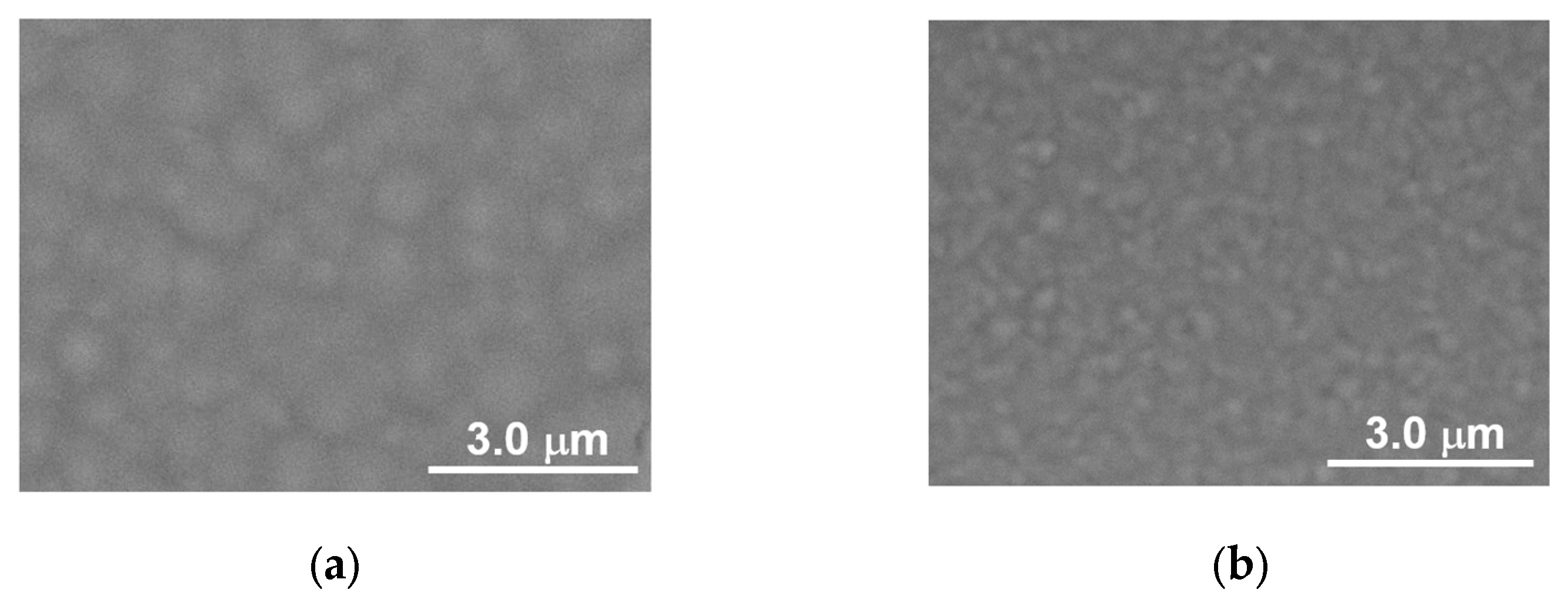
Figure 1 shows SEM images of Ga2O3 films grown on an α-Cr2O3 template and an α-Al2O3 substrate. In both cases, the film surfaces are relatively smooth and flat, indicating uniform film growth. Notably, the grain size of the Ga2O3 film grown on the α-Cr2O3 template is larger than that of the film grown on the α-Al2O3 substrate.
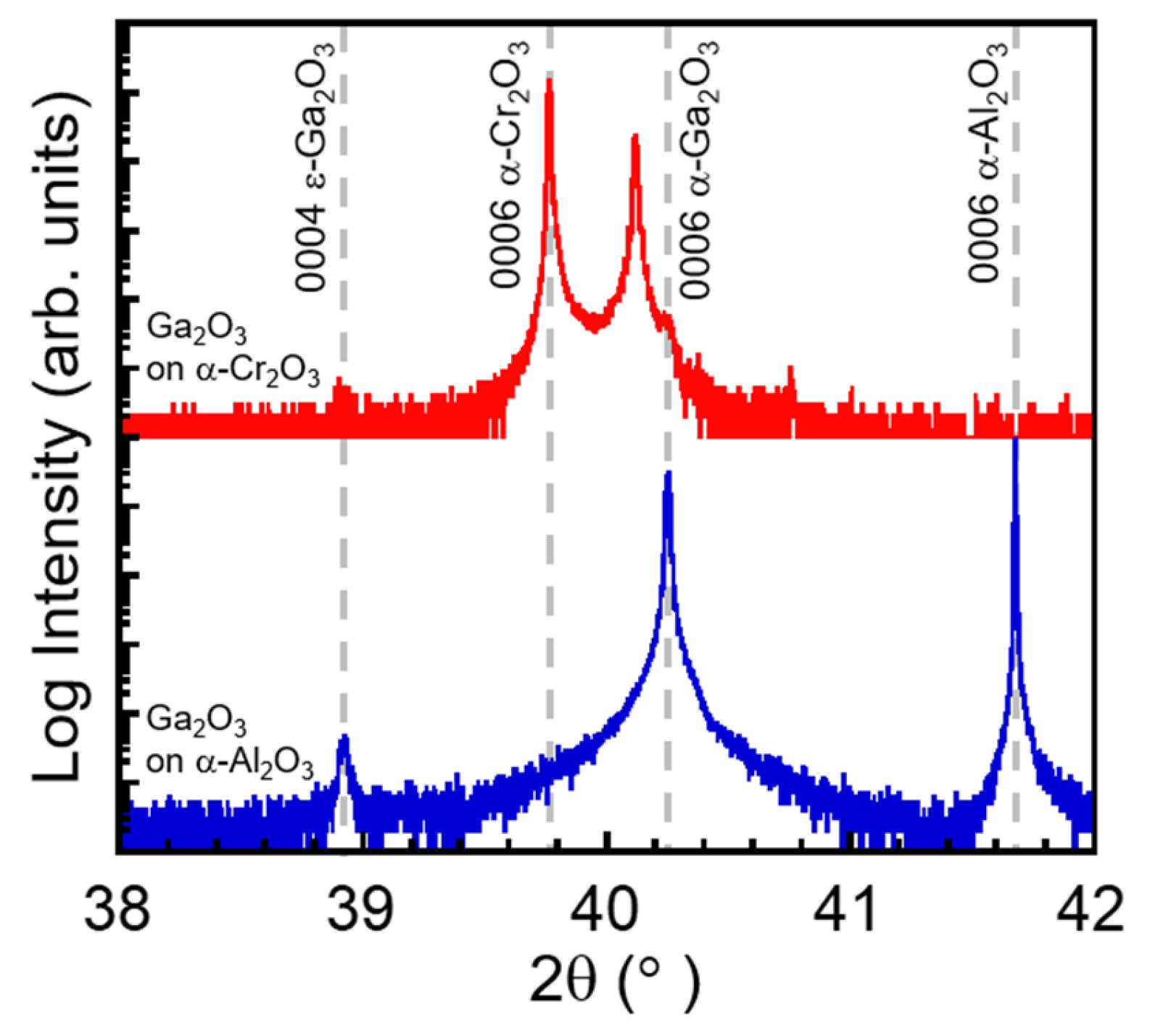
Figure 2 shows the results of the XRD θ-2θ measurements comparing Ga2O3 films grown on an α-Cr2O3 template and α-Al2O3 substrate. In addition to the peaks originating from the template or substrate, the main peak for (0006) α-Ga2O3 was observed in the XRD patterns of both samples. Although the samples also exhibited a smaller (0004) ε-Ga2O3 peak, its intensity was significantly suppressed in the sample grown on the α-Cr2O3 template. This result is in agreement with that of a previous report [28]. Furthermore, in the wider-range θ-2θ XRD scan (2θ = 10–70°), no additional diffraction peaks other than those described above were observed. As can be seen in Figure 2, the (0006) peak of α-Ga2O3 film grown on the α-Cr2O3 template shifted to a lower angle relative to that of the film grown on the α-Al2O3 substrate, whose peak position is close to the theoretical value. Using the asymmetric XRD measurements, the a-axis and c-axis lattice constants of α-Ga2O3 grown on the α-Cr2O3 template were found to be 4.948 Å and 13.476 Å, while the a-axis and c-axis lattice constants of the α-Ga2O3 grown on an α-Al2O3 substrate were 4.993 Å and 13.431 Å. In the sample grown on the α-Cr2O3 template, the a-axis lattice constant was smaller than that of α-Ga2O3 grown on an α-Al2O3 substrate and was nearly identical to the a-axis lattice constant of the α-Cr2O3 template itself, as presented in the Introduction. By contrast, the c-axis lattice constant was larger than that of α-Ga2O3 grown on an α-Al2O3 substrate. The latter is close to the theoretical value [40]. This clearly indicates that the α-Ga2O3 film grew coherently under strain on the α-Cr2O3 template. It should also be noted that the sample grown on the α-Cr2O3 template exhibited a slight shoulder peak at a higher angle, indicating the presence of a small amount of relaxed α-Ga2O3.
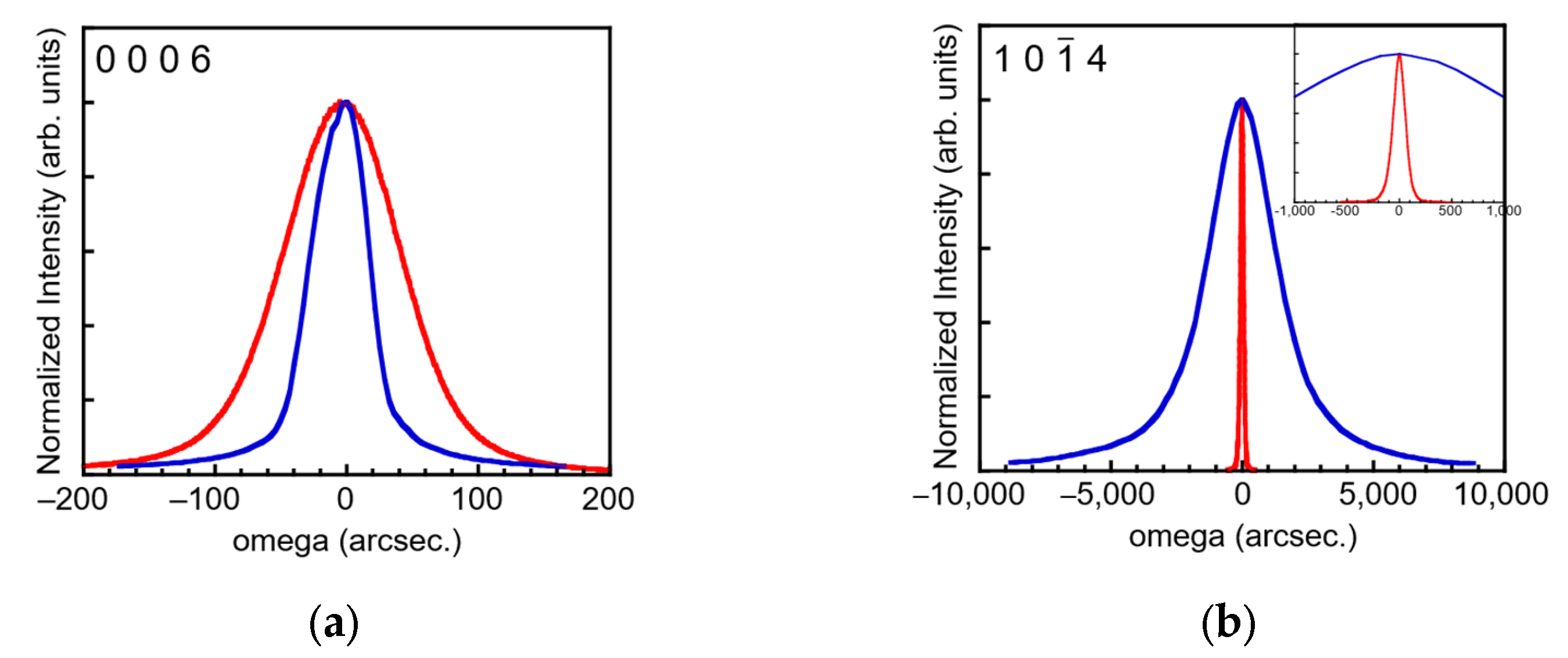
Figure 3 shows the (0006) and (10 1 ¯ 4) X-ray rocking-curve (XRC) profiles of α-Ga2O3 films grown on an α-Cr2O3 template and an α-Al2O3 substrate. Enlarged views of the (10 1 ¯ 4) XRC profiles are shown in the inset. The red and blue curves correspond to the α-Ga2O3 films grown on the α-Cr2O3 template and the α-Al2O3 substrate, respectively. For the (0006) symmetric reflection, the rocking-curve width of the film grown on the α-Cr2O3 template is slightly larger than that of the film grown on the α-Al2O3 substrate. In contrast, for the (10 1 ¯ 4) asymmetric reflection, the rocking-curve width is clearly narrower for the film grown on the α-Cr2O3 template.
Table 1 shows the (0006) and (10 1 ¯ 4) X-ray rocking-curve (XRC) full-width at half-maximum (FWHM) values of the α-Ga2O3 films grown on the α-Cr2O3 template and α-Al2O3 substrate. The values shown in parentheses are for (0006) and (10 1 ¯ 4) XRC FWHM values of the α-Cr2O3 template itself. As summarized in Table 1, the (0006) XRC FWHM values are 105 and 51 arcsec for the α-Ga2O3 films grown on the α-Cr2O3 template and the α-Al2O3 substrate, respectively. The corresponding (10 1 ¯ 4) XRC FWHM values are 135 and 3016 arcsec, respectively. The small twist distribution, reflected in the narrow (10 1 ¯ 4) XRC FWHM value, is attributed to the small lattice mismatch between α-Ga2O3 and α-Cr2O3. Furthermore, the XRC FWHM values of the α-Ga2O3 film on the α-Cr2O3 template are close to those of the α-Cr2O3 template itself.
The table also shows the screw dislocation density ( ρ screw ) and edge dislocation density ( ρ edge ) estimated from the XRC FWHM values using the following equation [24,27,31]:
ρ screw / edge = α 2 tilt / twist 2 π · ln 2 · b 2
where b is the length of each Burgers vector and α is the angle of the tilt/twist distribution. The Burgers vector b = 1 3 <2 1 ¯ 1 ¯ 0> was used for calculating tilt distribution, whereas b = <0001> was used for twist dislocations. The edge dislocation density was evaluated from the estimated FWHM of the (10 1 ¯ 0) reflection, which was obtained by extrapolation using Equation (2) from the FWHM values measured for multiple diffraction planes, including the (0001) and (10 1 ¯ 4) reflections [31].
β h kil 2 = β tilt cos χ 2 + β twist sin χ 2 .
Here, β denotes the FWHM of each reflection, and χ is the angle between the (0001) plane and the corresponding diffraction plane. The film grown on the α-Cr2O3 template had an estimated screw dislocation density of 3 × 106 cm−2 and edge dislocation density of 7 × 107 cm−2, while the sample grown on the α-Al2O3 substrate had an estimated screw dislocation density of 8 × 105 cm−2 and edge dislocation density of 3 × 1010 cm−2. The estimated dislocation densities in the sample grown on the α-Al2O3 substrate were in agreement with those reported previously [19,22,24,27,31,32], whereas the estimated edge dislocation density of the α-Ga2O3 film grown on the α-Cr2O3 template was much smaller (i.e., by a factor of ~500). The estimated screw and edge dislocation densities of the α-Ga2O3 film grown on the α-Cr2O3 template were nearly the same as those of the α-Cr2O3 template, as can be seen in Table 1.
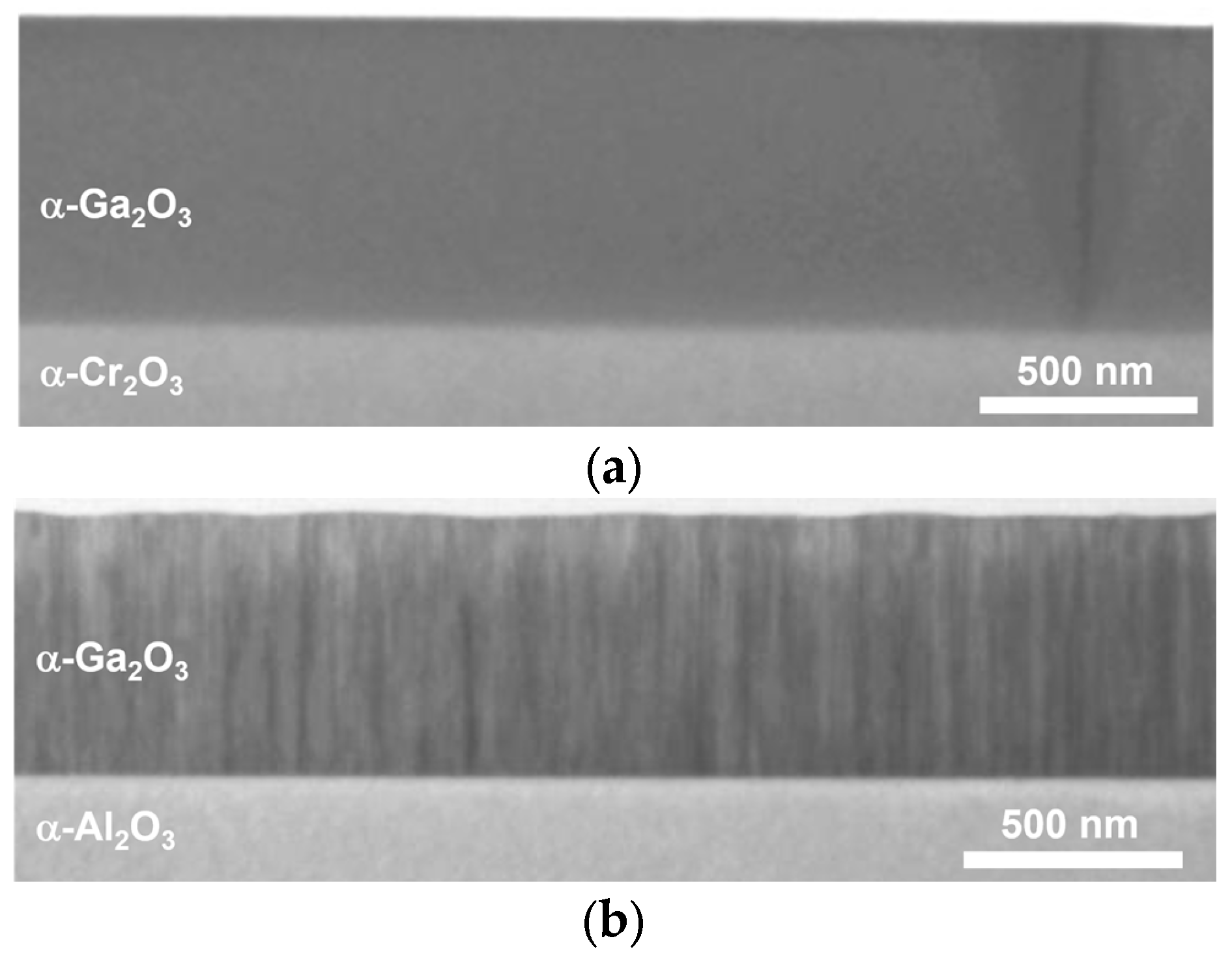
Figure 4 shows bright-field TEM images, captured at an acceleration voltage of 300 kV of the samples grown on the α-Cr2O3 template and α-Al2O3 substrate. As previously reported [19,22,24,27,32], a high density of dislocations in the order of 1010/cm2 was observed in the α-Ga2O3 film grown on the α-Al2O3 substrate, as shown in Figure 4b. In contrast, dislocations were rarely observed in the α-Ga2O3 film grown on the α-Cr2O3 templates, as shown in Figure 4a. The lamella used in this measurement was 500 nm thick, and there was a region more than a 2 μm wide in which no dislocations were found. The dislocation density could therefore be estimated to be below 108 cm−2, which is consistent with the value obtained from the XRD measurements (Table 1). It should be noted that a planar-like defect can be seen on the right side of the image in the sample grown on the α-Cr2O3 template. The presence of this defect may be related to the presence of a small amount of relaxed α-Ga2O3, as mentioned in Figure 2. The details of this defect, including its possible association with the relaxed phase, are currently under investigation.
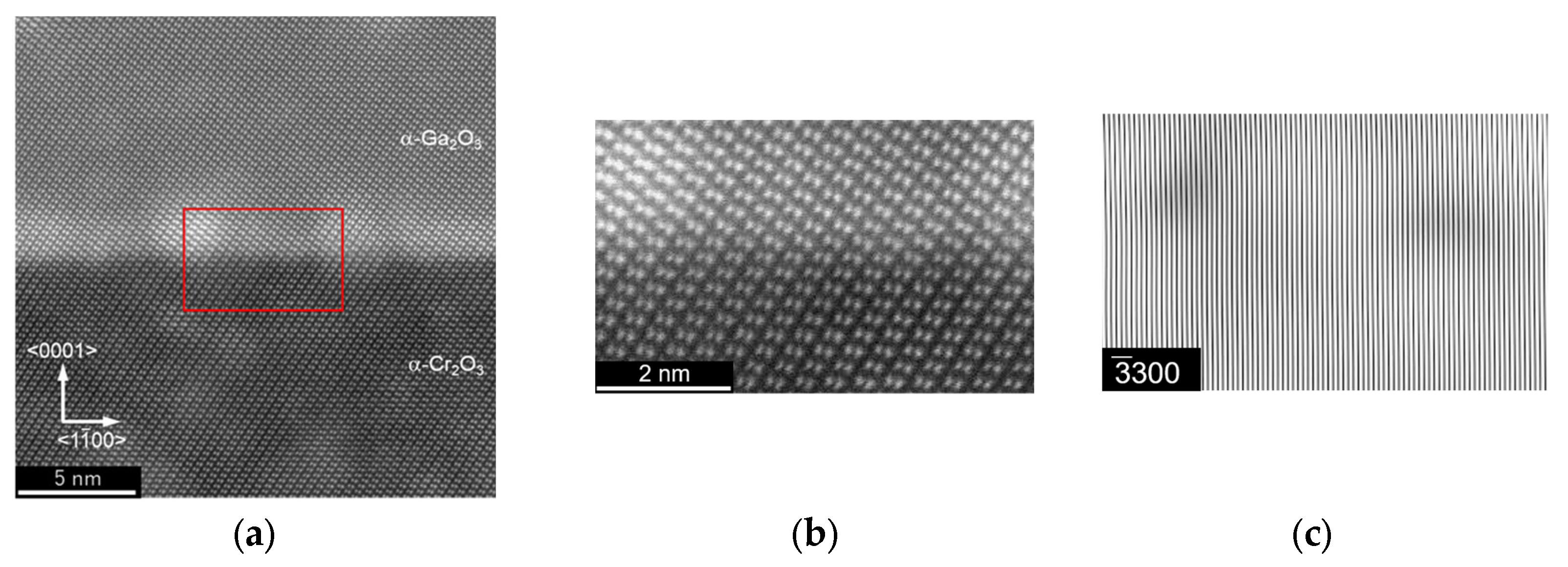
Figure 5a shows a high-angle annular dark-field scanning TEM (HAADF-STEM) image of the α-Ga2O3/α-Cr2O3 interface, and Figure 5b,c present an HAADF-STEM image and an inverse fast Fourier transform (FFT) image showing the ( 3 ¯ 300 ) plane, respectively, taken from the region indicated by the red square in Figure 5a. The cation lattices were perfectly matched between α-Ga2O3 and α-Cr2O3, and no variation in the number of atomic planes was observed across the interface. These results indicated that misfit dislocations were not generated at the α-Ga2O3/α-Cr2O3 interface in this region.
Thus, we succeeded in growing a high-quality α-Ga2O3 film with a dislocation density in the order of 107 cm−2, which is comparable to that of the α-Cr2O3 template. The dislocation density obtained in this study was much lower than that previously reported for α-Ga2O3 grown on α-Cr2O3 [28], indicating that the crystallinity of the α-Ga2O3 film strongly depends on that of the underlying α-Cr2O3. The realization of a higher-quality α-Cr2O3 underlayer, including bulk substrates, is therefore expected to enable further improvements in the α-Ga2O3 film quality.

4. Conclusions

In summary, we investigated the growth of α-Ga2O3 on the α-Cr2O3 template using mist CVD. The α-Ga2O3 film was coherently grown on the α-Cr2O3 template. Compared with the film grown on the α-Al2O3 substrate, the (10 1 ¯ 4) XRC FWHM value was significantly smaller. The screw and edge dislocation densities in the film, estimated from the XRC FWHM values, were 3 × 106 cm−2 and 7 × 107 cm−2, respectively. These values were almost the same as those of the α-Cr2O3 template used in this study. The HAADF-STEM and FFT images indicate that almost no misfit dislocations were generated at the α-Ga2O3/α-Cr2O3 interface. Thus, we succeeded in growing high-quality α-Ga2O3 films with low dislocation densities on an α-Cr2O3 template.

Author Contributions

K.Y.: Conceptualization, Methodology, Investigation, Writing—Original Draft, Writing—Review and Editing; S.X.: Conceptualization, Methodology, Investigation, Writing—Review and Editing; K.M.: Conceptualization, Methodology, Investigation, Writing—Review and Editing; R.I.: Investigation, Writing—Review and Editing; M.W.: Conceptualization, Methodology, Writing—Review and Editing, Supervision; T.T.: Conceptualization, Methodology, Writing—Review and Editing, Supervision; T.Y.: Conceptualization, Methodology, Investigation, Writing—Original Draft, Writing—Review and Editing, Supervision. All authors have read and agreed to the published version of the manuscript.

Funding

This research received no external funding.

Data Availability Statement

The data presented in this study must be requested from the corresponding author due to privacy constraints.

Acknowledgments

The authors would like to thank K. Rikitake, S. Takahashi and R. Yamada of Kogakuin University for their technical support in these experiments. The authors would also like to thank T. Onuma, K. Ogawa and T. Honda of Kogakuin University for engaging in fruitful discussions.

Conflicts of Interest

This research was carried out under a joint research collaboration between Kogakuin University and NGK INSULATORS, LTD. Authors Shiyu Xiao, Kazuto Murakami, Morimichi Watanabe, and Takahiro Tomita were employed by the company NGK INSULATORS, LTD. The authors declare no conflict of interest.

References

  1. Sabino, F.P.; de Oliveira, L.N.; Da Silva, J.L.F. Role of atomic radius and d-states hybridization in the stability of the crystal structure of M2O3 (M = Al, Ga, In) oxides. Phys. Rev. B 2014, 90, 155206. [Google Scholar] [CrossRef]
  2. Tippins, H.H. Optical Absorption and Photoconductivity in the Band Edge of β-Ga2O3. Phys. Rev. 1965, 140, A316. [Google Scholar] [CrossRef]
  3. Matsumoto, T.; Aoki, M.; Kinoshita, A.; Aono, T. Absorption and Reflection of Vapor Grown Single Crystal Platelets of β−Ga2O3. Jpn. J. Appl. Phys. 1974, 13, 1578. [Google Scholar] [CrossRef]
  4. Ueda, N.; Hosono, H.; Waseda, R.; Kawazoe, H. Anisotropy of electrical and optical properties in β-Ga2O3 single crystals. Appl. Phys. Lett. 1997, 71, 933. [Google Scholar] [CrossRef]
  5. Onuma, T.; Saito, S.; Sasaki, K.; Masui, T.; Yamaguchi, T.; Honda, T.; Higashiwaki, M. Valence band ordering in β-Ga2O3 studied by polarized transmittance and reflectance spectroscopy. Jpn. J. Appl. Phys. 2015, 54, 112601. [Google Scholar] [CrossRef]
  6. Geller, S. Crystal Structure of β-Ga2O3. J. Chem. Phys. 1960, 33, 676. [Google Scholar] [CrossRef]
  7. Ueda, N.; Hosono, H.; Waseda, R.; Kawazoe, H. Synthesis and control of conductivity of ultraviolet transmitting β-Ga2O3 single crystals. Appl. Phys. Lett. 1997, 70, 3561. [Google Scholar] [CrossRef]
  8. Víllora, E.G.; Shimamura, K.; Yoshikawa, Y.; Aoki, K.; Ichinose, N. Large-size β-Ga2O3 single crystals and wafers. J. Cryst. Growth 2004, 270, 420. [Google Scholar] [CrossRef]
  9. Aida, H.; Nishiguchi, K.; Takeda, H.; Aota, N.; Sunakawa, K.; Yaguchi, Y. Growth of β-Ga2O3 Single Crystals by the Edge-Defined, Film Fed Growth Method. Jpn. J. Appl. Phys. 2008, 47, 8506. [Google Scholar] [CrossRef]
  10. Kuramata, A.; Koshi, K.; Watanabe, S.; Yamaoka, Y.; Masui, T.; Yamakoshi, S. High-quality β-Ga2O3 single crystals grown by edge-defined film-fed growth. Jpn. J. Appl. Phys. 2016, 55, 1202A2. [Google Scholar] [CrossRef]
  11. Tomm, Y.; Reiche, P.; Klimm, D.; Fukuda, T. Czochralski grown Ga2O3 crystals. J. Cryst. Growth 2000, 220, 510. [Google Scholar] [CrossRef]
  12. Hoshikawa, K.; Ohba, E.; Kobayashi, T.; Yanagisawa, J.; Miyagawa, C.; Nakamura, Y. Growth of β-Ga2O3 single crystals using vertical Bridgman method in ambient air. J. Cryst. Growth 2016, 447, 36. [Google Scholar] [CrossRef]
  13. Oshima, T.; Arai, N.; Suzuki, N.; Ohira, S.; Fujita, S. Surface morphology of homoepitaxial β-Ga2O3 thin films grown by molecular beam epitaxy. Thin Solid Films 2008, 516, 5768. [Google Scholar] [CrossRef]
  14. Higashiwaki, M.; Sasaki, K.; Kuramata, A.; Masui, T.; Yamakoshi, S. Gallium oxide (Ga2O3) metal-semiconductor field-effect transistors on single-crystal β-Ga2O3 (010) substrates. Appl. Phys. Lett. 2012, 100, 013504. [Google Scholar] [CrossRef]
  15. Murakami, H.; Nomura, K.; Goto, K.; Sasaki, K.; Kawara, K.; Thieu, Q.T.; Togashi, R.; Kumagai, Y.; Higashiwaki, M.; Kuramata, A.; et al. Homoepitaxial growth of β-Ga2O3 layers by halide vapor phase epitaxy. Appl. Phys. Express 2015, 8, 015503. [Google Scholar] [CrossRef]
  16. Lee, S.; Kaneko, K.; Fujita, S. Homoepitaxial growth of beta gallium oxide films by mist chemical vapor deposition. Jpn. Appl. Phys. 2016, 55, 1202B8. [Google Scholar] [CrossRef]
  17. Shinohara, D.; Fujita, S. Heteroepitaxy of Corundum-Structured α-Ga2O3 Thin Films on α-Al2O3 Substrates by Ultrasonic Mist Chemical Vapor Deposition. Jpn. J. Appl. Phys. 2008, 47, 7311. [Google Scholar] [CrossRef]
  18. Segura, A.; Artús, L.; Cuscó, R.; Goldhahn, R.; Feneberg, M. Band gap of corundumlike α-Ga2O3 determined by absorption and ellipsometry. Phys. Rev. Mater 2017, 1, 024604. [Google Scholar] [CrossRef]
  19. Kaneko, K.; Kawanowa, H.; Ito, H.; Fujita, S. Evaluation of Misfit Relaxation in α-Ga2O3 Epitaxial Growth on α-Al2O3 Substrate. Jpn. J. Appl. Phys. 2012, 51, 020201. [Google Scholar] [CrossRef]
  20. Kawaharamura, T.; Dang, G.T.; Furuta, M. Successful Growth of Conductive Highly Crystalline Sn-Doped α-Ga2O3 Thin Films by Fine-Channel Mist Chemical Vapor Deposition. Jpn. J. Appl. Phys. 2012, 51, 040207. [Google Scholar] [CrossRef]
  21. Oshima, Y.; Vílllora, E.G.; Shimamura, K. Halide vapor phase epitaxy of twin-free α-Ga2O3 on sapphire (0001) substrates. Appl. Phys. Express 2015, 8, 055501. [Google Scholar] [CrossRef]
  22. Jinno, R.; Uchida, T.; Kaneko, K.; Fujita, S. Reduction in edge dislocation density in corundum-structured α-Ga2O3 layers on sapphire substrates with quasi-graded α-(Al,Ga)2O3 buffer layers. Appl. Phys. Express 2016, 9, 071101. [Google Scholar] [CrossRef]
  23. Oda, M.; Kaneko, K.; Fujita, S.; Hitora, T. Crack-free thick (~5 µm) α-Ga2O3 films on sapphire substrates with α-(Al,Ga)2O3 buffer layers. Jpn. J. Appl. Phys. 2016, 55, 1202B4. [Google Scholar] [CrossRef]
  24. Ma, T.C.; Chen, X.H.; Kuang, Y.; Li, L.; Li, J.; Kremer, F.; Ren, F.-F.; Gu, S.L.; Zhang, R.; Zheng, Y.D.; et al. On the origin of dislocation generation and annihilation in α-Ga2O3 epilayers on sapphire. Appl. Phys. Lett. 2019, 115, 182101. [Google Scholar] [CrossRef]
  25. Oshima, Y.; Kawara, K.; Shinohe, T.; Hitora, T.; Kasu, M.; Fujita, S. Epitaxial lateral overgrowth of α-Ga2O3 by halide vapor phase epitaxy. APL Mater. 2019, 7, 022503. [Google Scholar] [CrossRef]
  26. Uno, K.; Ohta, M.; Tanaka, I. Growth mechanism of α-Ga2O3 on a sapphire substrate by mist chemical vapor deposition using acetylacetonated gallium source solutions. Appl. Phys. Lett. 2020, 117, 052106. [Google Scholar] [CrossRef]
  27. Kim, B.; Yang, D.; Sohn, W.; Lee, S.; Choi, H.H.C.; Jang, T.; Yoon, E.; Park, Y.; Jang, H.W. Strain relaxation and dislocation annihilation in compositionally graded α-(AlxGa1-x)2O3 layer for high voltage α-Ga2O3 power devices. Acta Mater. 2021, 221, 117423. [Google Scholar] [CrossRef]
  28. Stepanov, S.I.; Nikolaev, V.I.; Almaev, A.V.; Pechnikov, A.I.; Scheglov, M.P.; Chikiryaka, A.V.; Kushnarev, B.O.; Polyakov, A.Y. HVPE growth of corundum-structured α-Ga2O3 on sapphire substrates with α-Cr2O3 buffer layer. Mater. Phys. Mech. 2021, 47, 577. [Google Scholar]
  29. Zhang, Y.J.; Wang, Z.P.; Kuang, Y.; Gong, H.H.; Hao, J.G.; Sun, X.Y.; Ren, F.-F.; Yang, Y.; Gu, S.L.; Zheng, Y.D.; et al. Dislocation dynamics in α-Ga2O3 micropillars from selective-area epitaxy to epitaxial lateral overgrowth. Appl. Phys. Lett. 2022, 120, 121601. [Google Scholar] [CrossRef]
  30. Oshima, Y.; Ando, H.; Shinohe, T. Reduction of dislocation density in α-Ga2O3 epilayers via rapid growth at low temperatures by halide vapor phase epitaxy. Appl. Phys. Express 2023, 16, 065501. [Google Scholar] [CrossRef]
  31. Takane, H.; Konishi, S.; Hayasaka, Y.; Ota, R.; Wakamatsu, T.; Isobe, Y.; Kaneko, K.; Tanaka, K. Structural characterization of threading dislocation in α-Ga2O3 thin films on c- and m-plane sapphire substrates. J. Appl. Phys. 2024, 136, 025105. [Google Scholar] [CrossRef]
  32. Yasuoka, T.; Susami, H.; Liu, L.; Dang, G.T.; Kawaharamura, T. Analysis of dislocation defects in compositionally step-graded α-(AlxGa1-x)2O3 layers. RSC Adv. 2024, 14, 31570. [Google Scholar] [CrossRef] [PubMed]
  33. Yang, D.; Kim, B.; Eom, T.H.; Park, Y.; Jang, H.W. Epitaxial growth of alpha gallium oxide thin films on sapphire substrates for electronic and optoelectronic devices: Progress and perspective. Electron. Mater. Lett. 2022, 18, 113. [Google Scholar] [CrossRef]
  34. Biswas, M.; Nishinaka, H. Thermodynamically metastable α-, ε- (or κ-), and γ-Ga2O3: From material growth to device applications. APL Mater. 2022, 10, 060701. [Google Scholar] [CrossRef]
  35. Oshima, Y.; Ahmadi, E. Progress and challenges in the development of ultra-wide bandgap semiconductor α-Ga2O3 toward realizing power device applications. Appl. Phys. Lett. 2022, 121, 260501. [Google Scholar] [CrossRef]
  36. Kaneko, K.; Fujita, S.; Shinohe, T. Progress in α-Ga2O3 for practical device applications. Jpn. J. Appl. Phys. 2023, 62, SF0803. [Google Scholar] [CrossRef]
  37. Mondal, A.K.; Ping, L.K.; Haniff, M.A.S.M.; Bahru, R.; Mohamed, M.A. Recent Advancements in α-Ga2O3 Thin Film Growth for Power Semiconductor Devices via Mist CVD Method: A Comprehensive Review. Cryst. Res. Technol. 2024, 59, 2300311. [Google Scholar] [CrossRef]
  38. Usui, A.; Sunakawa, H.; Sakai, A.; Yamaguchi, A.A. Thick GaN Epitaxial Growth with Low Dislocation Density by Hydride Vapor Phase Epitaxy. Jpn. J. Appl. Phys. 1997, 36, L899. [Google Scholar] [CrossRef]
  39. Kaneko, K.; Nomura, T.; Fujita, S. Corundum-structured α-phase Ga2O3-Cr2O3-Fe2O3 alloy system for novel functions. Phys. Status Solidi C 2010, 7, 2467. [Google Scholar] [CrossRef]
  40. Marezio, M.; Remeika, J.P. Bond Lengths in the α-Ga2O3 Structure and the High-Pressure Phase of Ga2-xFexO3. J. Chem. Phys. 1967, 46, 1862. [Google Scholar] [CrossRef]
Figure 1. SEM images of Ga2O3 films grown on (a) α-Cr2O3 template and (b) α-Al2O3 substrate.
Crystals 16 00193 g001
Figure 2. Results of XRD θ-2θ measurements of Ga2O3 films grown on α-Cr2O3 template (red) and α-Al2O3 substrate (blue).
Crystals 16 00193 g002
Figure 3. XRC profiles of α-Ga2O3 films grown on α-Cr2O3 template (red) and α-Al2O3 substrates (blue): (a) (0006) symmetric reflection and (b) (10 1 ¯ 4) asymmetric reflection (inset: enlarged views of (10 1 ¯ 4) XRC profiles).
Crystals 16 00193 g003
Figure 4. Bright-field TEM images of Ga2O3 films grown on (a) α-Cr2O3 template and (b) α-Al2O3 substrate.
Crystals 16 00193 g004
Figure 5. HAADF-STEM images of (a) wide area and (b) enlarged area marked in red square of (a) at α-Ga2O3/α-Cr2O3 interface, and (c) inverse FFT image showing ( 3 ¯ 300 ) plane of (b).
Crystals 16 00193 g005
Table 1. Measured (0006) and (10 1 ¯ 4) XRC FWHM values and estimated dislocation densities of α-Ga2O3 films grown on an α-Cr2O3 template and α-Al2O3 substrate. The dislocation density was calculated using Equations (1) and (2) using extrapolated (10 1 ¯ 0) XRC FWHM derived from the FWHM values of multiple diffraction planes. Values in parentheses correspond to those of the α-Cr2O3 template and are shown as reference values.
XRC FWHM
(Arcsec.)
Estimated Dislocation Density
(cm−2)
000610 1 ¯ 4ScrewEdge
α-Ga2O3 film
on α-Cr2O3 template
1051353 × 1067 × 107
(95)(117)(3 × 10⁶)(6 × 10⁷)
α-Ga2O3 film
on α-Al2O3 substrate
5130168 × 1053 × 1010
Disclaimer/Publisher’s Note: The statements, opinions and data contained in all publications are solely those of the individual author(s) and contributor(s) and not of MDPI and/or the editor(s). MDPI and/or the editor(s) disclaim responsibility for any injury to people or property resulting from any ideas, methods, instructions or products referred to in the content.