1. Introduction
The dark current–voltage (I–V) response is a fundamental diagnostic tool for solar cells. It enables the evaluation of junction integrity and the quantification of internal electrical losses [
1]. Such measurements provide valuable insights into recombination processes, barrier inhomogeneities, and series resistance effects, thereby enabling a more accurate evaluation of junction quality. Moreover, dark I–V analysis offers a straightforward and reliable approach for probing the electrical behavior of the p–n junction, making it indispensable for both research studies and device optimization [
2,
3,
4]. Metal–insulator–semiconductor (MIS) devices, such as Ag/pSiO
2/Si structures, offer several advantages over conventional p–n junction solar cells. These include simpler fabrication processes, higher breakdown voltage capabilities, and potentially higher yields [
5,
6]. These devices display behavior similar to conventional p–n junctions under dark conditions, suggesting that the MIS structure can effectively replicate junction-like electrical performance [
7,
8,
9,
10]. A key focus of our analysis is the impact of thermally grown SiO
2 on porous silicon (PS) layers and how this oxidation process influences the electrical behavior of the cells [
11,
12]. The oxide layer plays a significant role in surface passivation, charge transport, and overall cell performance [
13,
14]. The electrical behavior of these devices can be modeled by the standard diode equation [
15,
16], extended to include the effects of the parasitic Rs and Rsh. The current–voltage relationship is expressed in Equation (1):
where I and V are the output current and voltage, Is is the diode saturation current, n is the ideality factor, q is the electron charge, k is the Boltzmann constant, T is the temperature, Rs represents the series resistance, and Rsh denotes the shunt resistance. This model allows for a more realistic representation of real solar cell behavior, enabling the extraction of key electrical parameters that indicate device quality and efficiency losses due to fabrication or material issues.
For thermionic emission, the Richardson equation [
17] describes how the emitted current density J (in A/m
2) depends on the temperature T of the emitting material. This relationship is expressed by the following equation:
In this equation, J is the thermionic current density (A/m
2), T is the absolute temperature of the emitting surface (in Kelvin), W is the work function of the material (in electron volts, eV), q is the elementary charge (1.602 × 10
−19 C), k is the Boltzmann constant (1.381 × 10
−23 J/K) and A
G is the Richardson constant (also known as the Richardson–Dushman constant), typically 1.2 × 10
6 A/m
2 K
2 for metals. The exponential term exp(−qW/KT) indicates the strong temperature dependence of the emission process. As the temperature increases, the number of electrons with sufficient energy to overcome the work function barrier also increases, causing a rapid rise in the current density. At high temperatures, the current density becomes approximately proportional to T
2, as described by the pre-exponential term in the equation. The Richardson equation is fundamental in understanding electron emission from metals and plays a crucial role in the design and modeling of various electronic and optoelectronic devices, including vacuum tubes, Schottky diodes, thermionic converters, and metal–insulator–semiconductor (MIS) structures [
18].
Understanding the dark I–V characteristics is crucial for identifying the dominant carrier transport mechanisms, which may shift from tunneling to thermionic emission depending on the temperature and interface quality [
19].
Motivated by previous reports on the temperature-dependent electrical transport and optoelectronic properties of MIS heterojunctions [
19,
20], as well as the influence of the annealing temperature on their structural and electrical parameters [
21], this study investigates the dark I–V characteristics of Ag/pSiO
2/Si MIS solar cells [
22] as a function of the temperature. The analysis aims to extract the series resistance (Rs) and shunt resistance (Rsh) and to identify the dominant carrier transport mechanisms. Rapid thermal processing (RTP) was employed for porous silicon oxidation, and the resulting electrical and optical properties of the MIS heterojunctions were examined to evaluate the effect of the oxidation temperature. The MIS structures were characterized through measurements of reflectance, dark current–voltage (I–V) characteristics, and extraction of key electrical parameters, such as the series Rs and Rsh, in order to evaluate the influence of the oxidation temperature on device performance.
2. Materials and Methods
For the fabrication of the pSiO
2Si device used in this study, we employed a p-type Czochralski-grown (Cz) silicon wafer as the starting material [
23].
The wafer had a thickness of approximately 330 µm and a resistivity in the range of 0.5–3 Ω·cm, suitable for forming a well-defined junction. The wafer was first diced into small square samples, each measuring 2 cm × 2 cm, to facilitate uniform processing and characterization. Before any surface treatment, the samples were subjected to a standard chemical cleaning process using the CP
4 solution, a mixture of nitric acid (HNO
3, 68%), hydrofluoric acid (HF, 40%), and acetic acid (CH
3COOH) in a volume ratio of 4:16:20, which is available from Sigma-Aldrich (Saint Louis, MO, USA). The CP
4 etchant was used for surface cleaning, as it effectively removes the damaged layers caused by mechanical polishing and dicing. This treatment results in a clean, defect-free surface suitable for subsequent porous silicon (PS) formation. The etching process is typically performed for about 30 s at room temperature, which is the standard condition to eliminate the mechanically damaged layer without inducing excessive wafer thinning. After etching, the samples were thoroughly rinsed with deionized water and dried using a nitrogen (N
2) gas jet to prevent surface oxidation and particle contamination. This preparation step ensured a clean and reactive silicon surface, necessary for the subsequent electrochemical porosification and thermal oxidation steps. Porous silicon (PS) layers [
24,
25,
26] were fabricated via electrochemical anodization [
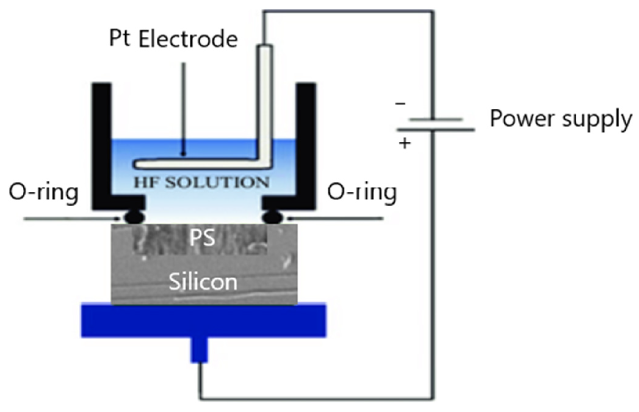
27] of (100)-oriented p-type monocrystalline silicon substrates with resistivity ranging from 0.5 to 3 Ω·cm. The anodization process shown in
Figure 1 was carried out in an electrolyte solution containing 20% HF, prepared by mixing hydrofluoric acid (HF, 40%), deionized water (H
2O), and ethanol (C
2H
5OH) in a volume ratio of 3:1:2. A constant anodization current density of 20 mA·cm
−2 was applied for 10 min to obtain uniform porous silicon films with consistent morphology and porosity.
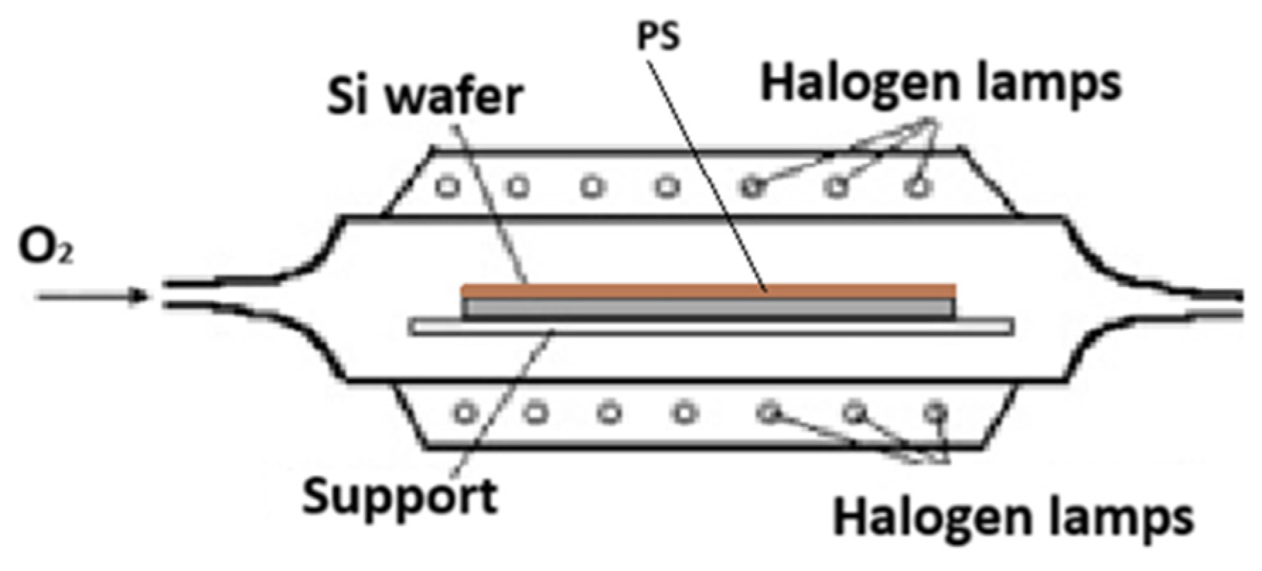
The PS was oxidized by IR-RTP at different oxidation temperatures (
Figure 2), ranging from 200 to 950 °C, under an oxygen atmosphere. For the thermal oxidation step, six wafers were processed at different oxidation temperatures, with the reported results based on a single sample per temperature. To ensure repeatability and assess the layer uniformity, three measurements were taken on each sample at three different locations on the wafer, all under identical conditions within the rapid thermal processing (RTP) system. This approach helps demonstrate the uniformity and consistency of the oxide layers across the wafer. Five of them were subjected to thermal annealing in an infrared furnace at different oxidation temperatures: 200 °C, 400 °C, 600 °C, 800 °C, and 950 °C, respectively. Annealing was performed under a pure oxygen (O
2) atmosphere, with the O
2 gas flow rate set to 10 ppm, for a fixed duration of 10 min, to grow silicon dioxide (SiO
2) layers on the porous silicon surfaces. The sixth wafer was kept untreated to serve as a reference sample for comparison. This controlled oxidation process allowed investigation of the effect of thermal treatment on the structural and electrical properties of the pSiO
2 layers.
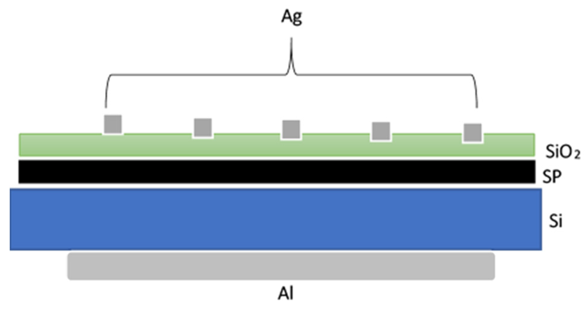
After the oxidation of porous silicon (resulting in a pSiO
2 structure), metallic contacts were deposited on both sides of the device to ensure proper electrical connectivity. Aluminum (Al) was used as the back contact, applied to the unstructured side of the silicon wafer to form an ohmic contact with the p-type substrate. Silver (Ag) served as the front contact, deposited on the surface of the porous silicon or pSiO
2 layer, enabling efficient current collection while preserving good optical transmittance. The layout of these metal contacts is illustrated in
Figure 3. The selection of Al and Ag was based on their excellent electrical conductivity and compatibility with standard silicon device fabrication processes.
For electrical characterization, dark current–voltage (I–V) measurements were performed to extract the key parameters of the device, namely the Rs and Rsh. These parameters are crucial for evaluating the diode’s quality and the overall performance of the photovoltaic structure. The Rs reflects the internal resistive losses within the device, while the Rsh indicates the degree of electrical isolation and leakage across the junction. Variations in these parameters help assess the impact of thermal oxidation and surface modification on the electrical behavior of the structure.
The surface structures were analyzed by a scanning electron microscope (JEOL JSM-5400, Tokyo, Japan). UV–vis–NIR spectrophotometer (Perkin-Elmer Lambda 950, Springfield, IL, USA) equipment measured the reflectance with an integrating sphere in the 250–1200 nm wavelength range. The Rs and Rsh were extracted from the dark I–V characteristics using the differential method.
3. Results and Discussion
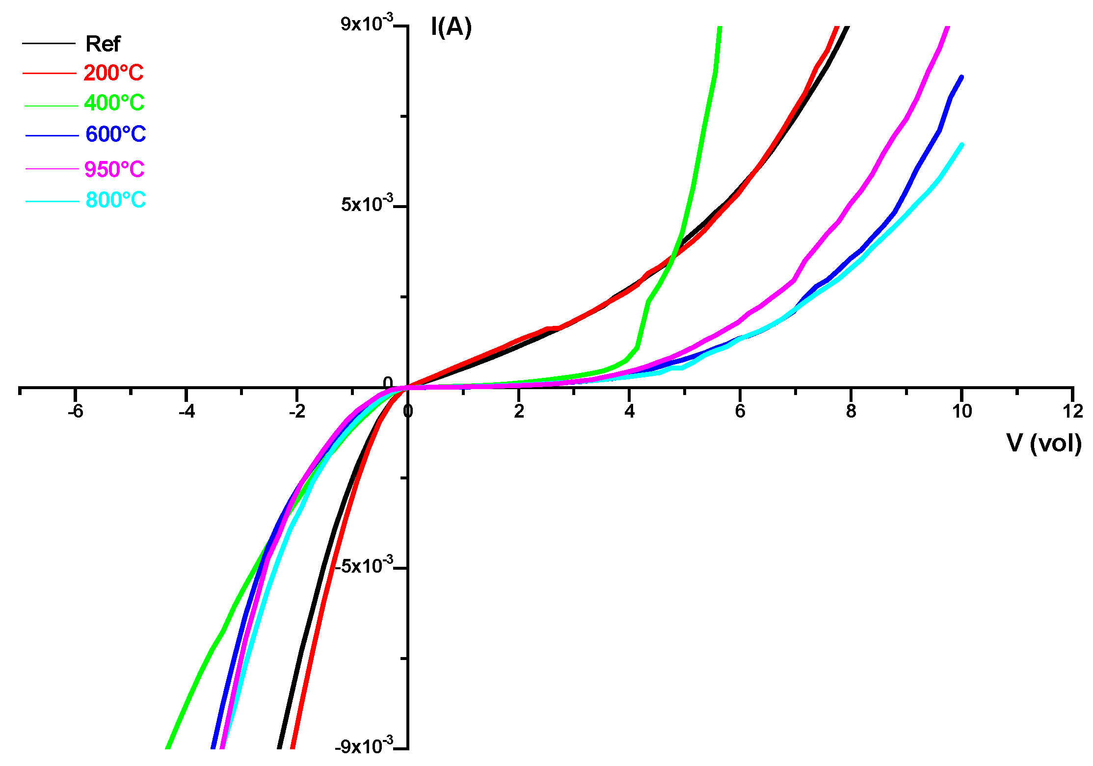
Figure 4 shows the morphology of the samples using a scanning electron microscope (SEM). We produced top and cross-section SEM images of the sample during 800 °C heat treatment. The SEM images reveal both the surface porosity and layer thickness. To determine the optimal annealing temperature for diode performance, we compared the dark current–voltage (I–V) characteristics of treated and untreated samples (
Figure 5). After that, we deduced an enhancement of the diode structure as the annealing temperature increases, which corresponds to a 400 °C temperature. When the heat treatment increases the pSiO
2 width, an increase in reflectivity is observed.
Figure 4 shows the cross-sectional morphologies of samples annealed at 200 °C, 400 °C, and 800 °C, which were examined to better understand the layer compositions. The results indicate that increasing the heat treatment temperature significantly increases the pSiO
2 layer thickness due to the enhanced thermal oxidation of porous silicon. At 200 °C, the oxide layer remains relatively thin. At 400 °C, the oxide layer slightly thickens, leading to lower reflectance, improved light absorption, and enhanced electrical properties, as evidenced by the reduced Rs and increased Rsh, indicating superior junction quality. In contrast, at 800 °C, the oxide layer becomes thicker and more continuous; however, excessive growth and potential structural degradation can weaken its insulating properties, increase leakage, and result in lower Rsh, thereby degrading the overall device performance.
The current–voltage (I–V) characteristics measured under dark conditions are fundamental for evaluating junction quality and diagnosing internal electrical losses. A key focus of this analysis is the extraction of the Rs and Rsh, both of which critically influence device performance. The Rs encompasses resistive losses arising from the bulk semiconductor, metal–semiconductor contact resistance, and interconnecting layers, and a high Rs results in voltage drops that degrade the fill factor (FF) and overall power conversion efficiency (PCE), especially under high illumination. In contrast, the Rsh represents parasitic leakage pathways due to structural defects, pinholes, or poor interface quality, and a low Rsh leads to increased leakage current at low voltages, reducing the open-circuit voltage (Voc) and efficiency. In the dark I–V curve, the Rs affects the slope at high forward bias where Ohmic behavior dominates, while the Rsh influences the low-voltage region near the origin where deviations from ideal diode behavior appear. Although recombination–generation currents contribute to the diode response, their impact on the conversion efficiency is typically minor compared to the resistive effects, particularly in both conventional p–n junction and minority-carrier MIS (metal–insulator–semiconductor) solar cells, where thermally treated SiO2 layers enhance the oxide quality and favor diffusion-dominated current transport. In work to extract the Rs and Rsh, differential methods such as the dV/dI technique are widely used: the Rs is estimated from the high-current region where the slope becomes linear (Rs ≈ dV/dI), and the Rsh is derived from the near-zero bias region (Rsh ≈ V/I). For more precise modeling, non-linear curve fitting can simultaneously yield the Rs, Rsh, ideality factor, and saturation current, offering comprehensive insight into diode behavior and process quality. A high Rs often indicates poor contact, insufficient doping, or damaged conductive paths, while a low Rsh points to defects or contamination, both of which impair device efficiency and reliability. Thus, accurate determination of the Rs and Rsh from dark I–V analysis is essential for identifying fabrication issues, guiding process optimization, and ensuring long-term device performance.
From the I–V characteristics in the dark for different temperatures in the range 200–950 °C of the pSiO
2/Si diode, as shown in
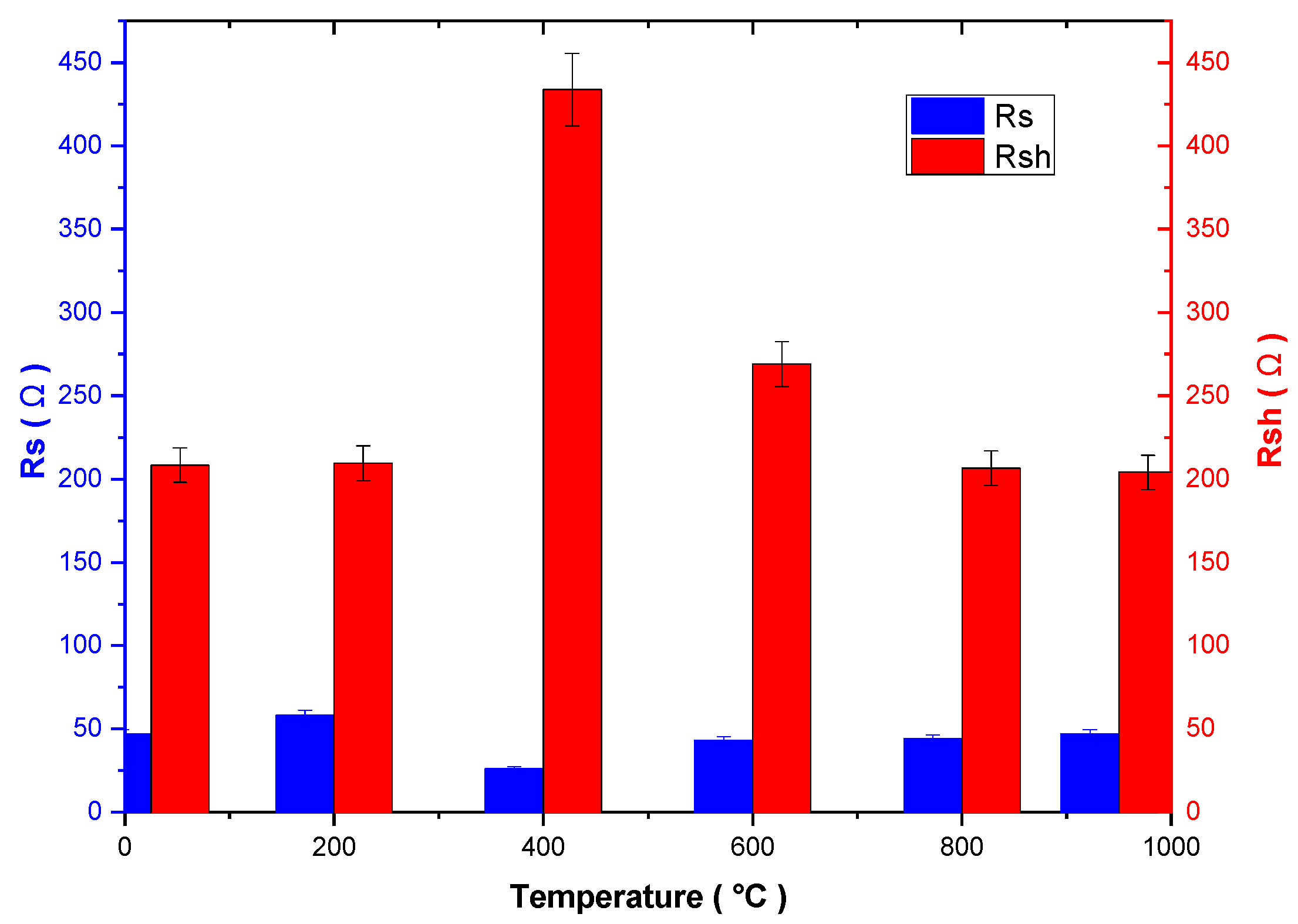
Figure 5, we extract the Rs and Rsh values by the differential method. The evolution of the Rs and Rsh with the oxidation temperature is illustrated in
Figure 6, highlighting the critical influence of thermal oxidation on electrical properties.
During our investigation of
Figure 6, we observed a significant reduction in the Rs at an annealing temperature of 400 °C, indicating improved electrical contact and enhanced carrier transport within the device, beyond which the Rs tends to stabilize. This reduction can be attributed to improved crystallinity and enhanced metal–semiconductor contact quality, both of which promote more efficient charge carrier transport across the junction. At the same temperature, an increase in the Rsh was also recorded, suggesting suppression of leakage pathways and improved junction isolation. However, further morphological analysis revealed that current leakage became more pronounced with increasing porosity of the porous silicon layer.
Maintaining a controlled porosity level through precise thermal oxidation treatment of porous silicon is essential for achieving an optimal balance between the device’s optical and electrical properties (
Figure 6). Thermal oxidation alters the surface and internal structure of the porous layer by growing a uniform, conformal silicon dioxide (pSiO
2) layer, which passivates surface defects and improves stability. This modification can significantly enhance the overall photo-response of the solar cell. However, when the porosity becomes excessive, it severely undermines both the mechanical and electrical integrity of the PS layer and the underlying p–n junction. A highly porous structure weakens the PS network, increasing its susceptibility to metal infiltration, particularly from top metal contacts such as silver (Ag) during deposition or subsequent processing steps. Such metal penetration can reach the active junction area or spread to the edges of the substrate, creating unintended conductive pathways that result in local shunting, leakage currents, and deterioration of the diode’s electrical characteristics.
This degradation is reflected in the electrical parameters: while the Rs may temporarily decrease due to the formation of more direct conductive paths, the Rsh drops significantly because of the proliferation of leakage currents. These changes lead to a decline in the critical performance of the cell, including the open-circuit voltage, fill factor, and overall power conversion efficiency. Moreover, metal-induced shunting accelerates device aging and increases the risk of early failure under real operating conditions.
Controlled porosity preserves light trapping, ensures junction stability, and optimizes the Rs and Rsh, improving solar cell performance and reliability.
As shown in
Figure 6, at the optimal oxidation temperature of 400 °C, the average Rs was 26.2 Ω (±1.3 Ω), while the average Rsh was 433.7 Ω (±21.5 Ω). These uncertainties demonstrate the consistency of the electrical measurements and confirm the reliability of the extracted parameters. Furthermore, the low optical reflectivity of 6% aligns with a porosity of 55%, as determined by the gravimetric (double-weight) method. The low Rs indicates efficient carrier transport, while the high Rsh reflects reduced leakage currents and effective junction isolation. However, large Rs values result in resistive power losses within the solar cell, whereas a low Rsh causes additional power losses by providing an alternate pathway for the photogenerated current. Furthermore, the reduced reflectivity confirms the effectiveness of the oxidized porous silicon surface in suppressing optical losses and enhancing light trapping, both of which are crucial for increasing the photocurrent and improving the overall efficiency of the solar cell.
Table 1 summarizes the average reflectance values over the 400–800 nm range for each oxidation temperature, along with the standard deviations.
As shown in
Table 1, the reflectance was measured at different oxidation temperatures to investigate its correlation with the Rs and Rsh.
The results demonstrate that changes in reflectance with varying oxidation temperatures are closely linked to modifications of the surface morphology and nanostructure of the oxidized porous silicon (pSiO2) layer. These structural changes have a significant impact on the electrical performance of the device.
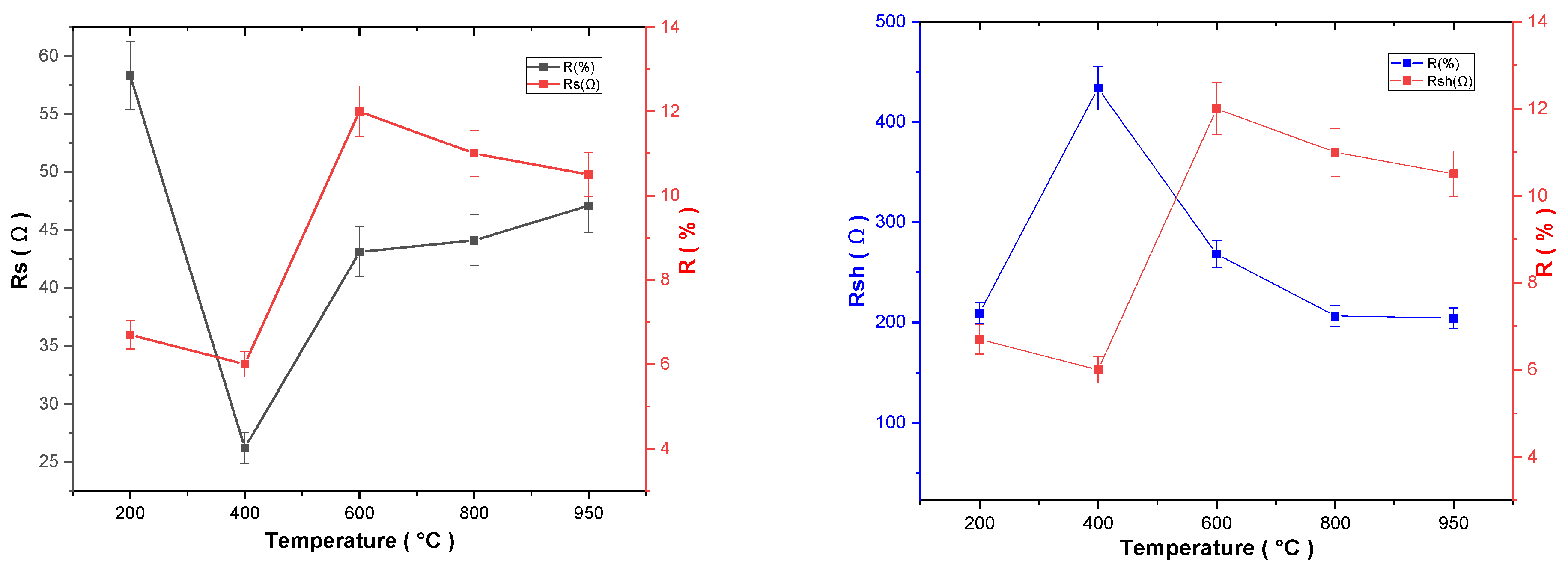
At an oxidation temperature of 400 °C, the reflectance decreases to 6%, indicating improved light absorption. This improvement in optical behavior corresponds to better electrical characteristics, including a reduction in the Rs and an increase in the Rsh, reflecting improved junction quality and reduced leakage.
However, at higher oxidation temperatures, excessive oxide growth and potential structural degradation may occur, leading to deterioration of the insulating properties and the possible diffusion of metal contacts into the junction. These effects increase the leakage currents and result in a reduction of the Rsh, negatively impacting the overall device performance.
Figure 7 illustrates the correlation between the reflectance and the electrical parameters (Rs and Rsh). From
Figure 7, we observed a strong correlation between the optical and electrical properties: reduced reflectance was linked to enhanced light absorption, improved junction quality, lower Rs, and higher Rsh. This highlights the importance of optimizing the oxidation temperature to simultaneously minimize optical losses and enhance electrical performance. The pSiO
2 layer exhibited a thickness of 150 ± 15 nm at 400 °C, as measured by a profilometer, which is sufficiently large to block electron transport to the Ag front contact.
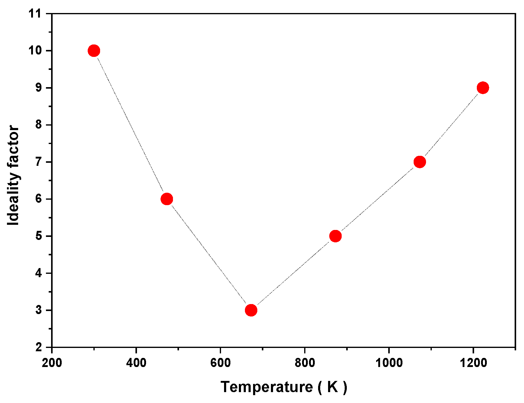
The temperature-dependence of the ideality factor estimated from the forward I–V characteristics using the thermionic emission model is showed in
Figure 8. For an ideal diode, the ideality factor (η) should be equal to 1. In the present case, η decreases as the temperature increases from 300 K to 673 K, indicating improved transport dominated by ideal thermionic emission and the reduced influence of defects and secondary mechanisms such as recombination via interface states. Above 673 K, however, η increases again with the temperature due to the predominance of non-ideal transport mechanisms, including barrier height inhomogeneities caused by microscopic variations in the material composition, increased recombination via activated interface states, higher series resistance, and the coexistence of multiple transport mechanisms, such as thermionic–field emission. These effects collectively lead to significant deviations from ideal behavior and account for the observed high ideality factors [
19,
20].
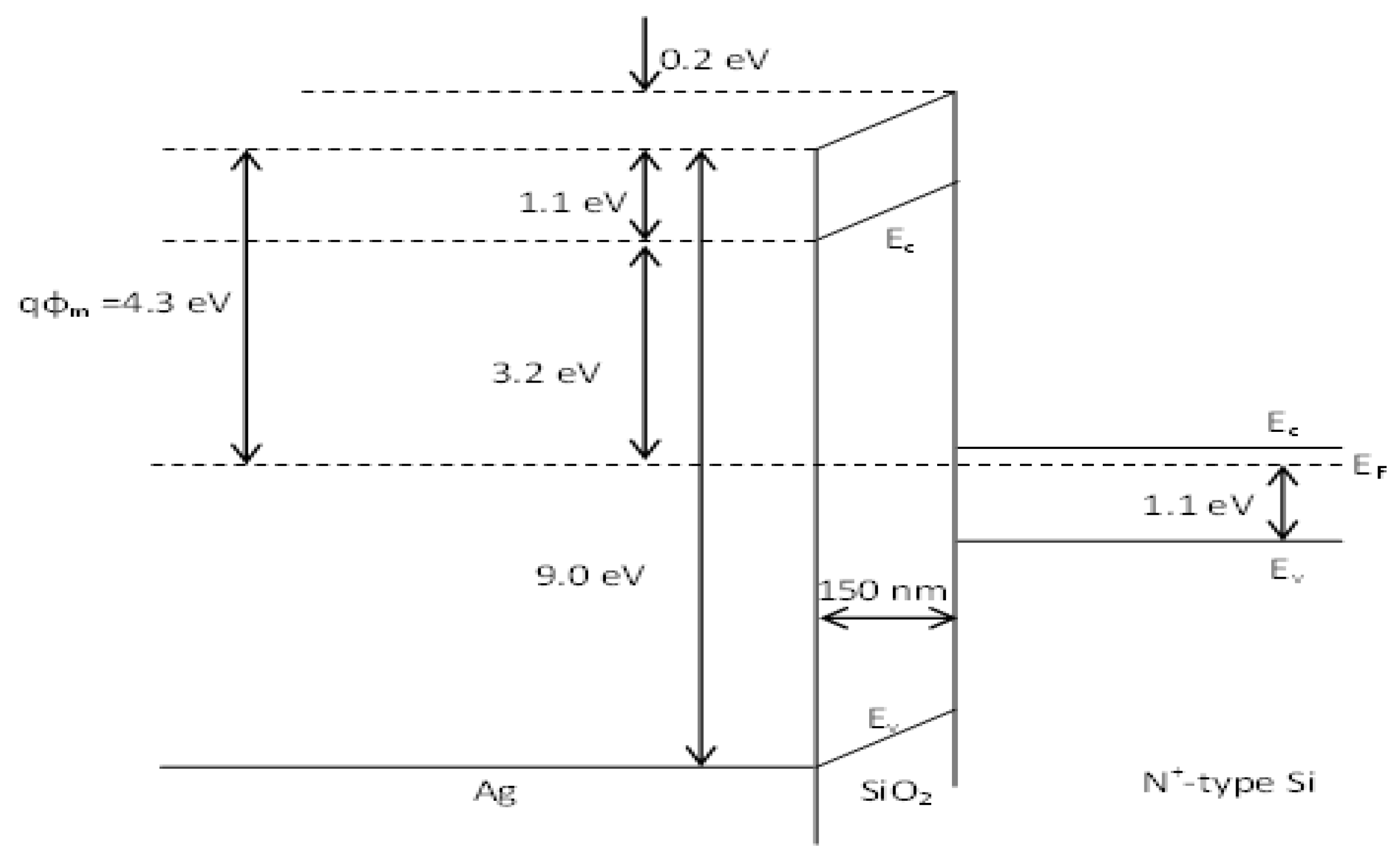
Hence, under these conditions, when we consider the energy band diagram in
Figure 9, we can assume that the sole possible current mechanism is thermionic. However, the tunneling contribution is very weak. Consequently, and by neglecting defects’ effect on pSiO
2, instead of a current flow over a metal–Si interface, electrons have to overcome a potential barrier of 3.2 eV to reach the metallic contact. In addition, the conductivity of electrons in a thick pSiO
2 layer is small enough, leading to an important recombination rate. Therefore, the photocurrent of the PV cell drastically diminishes, leading to a decrease in the open-circuit voltage and the rest of the electrical characteristics of the solar cell [
28].
