
Towards AZO Thin Films for Electronic and Optoelectronic Large-Scale Applications


Abstract
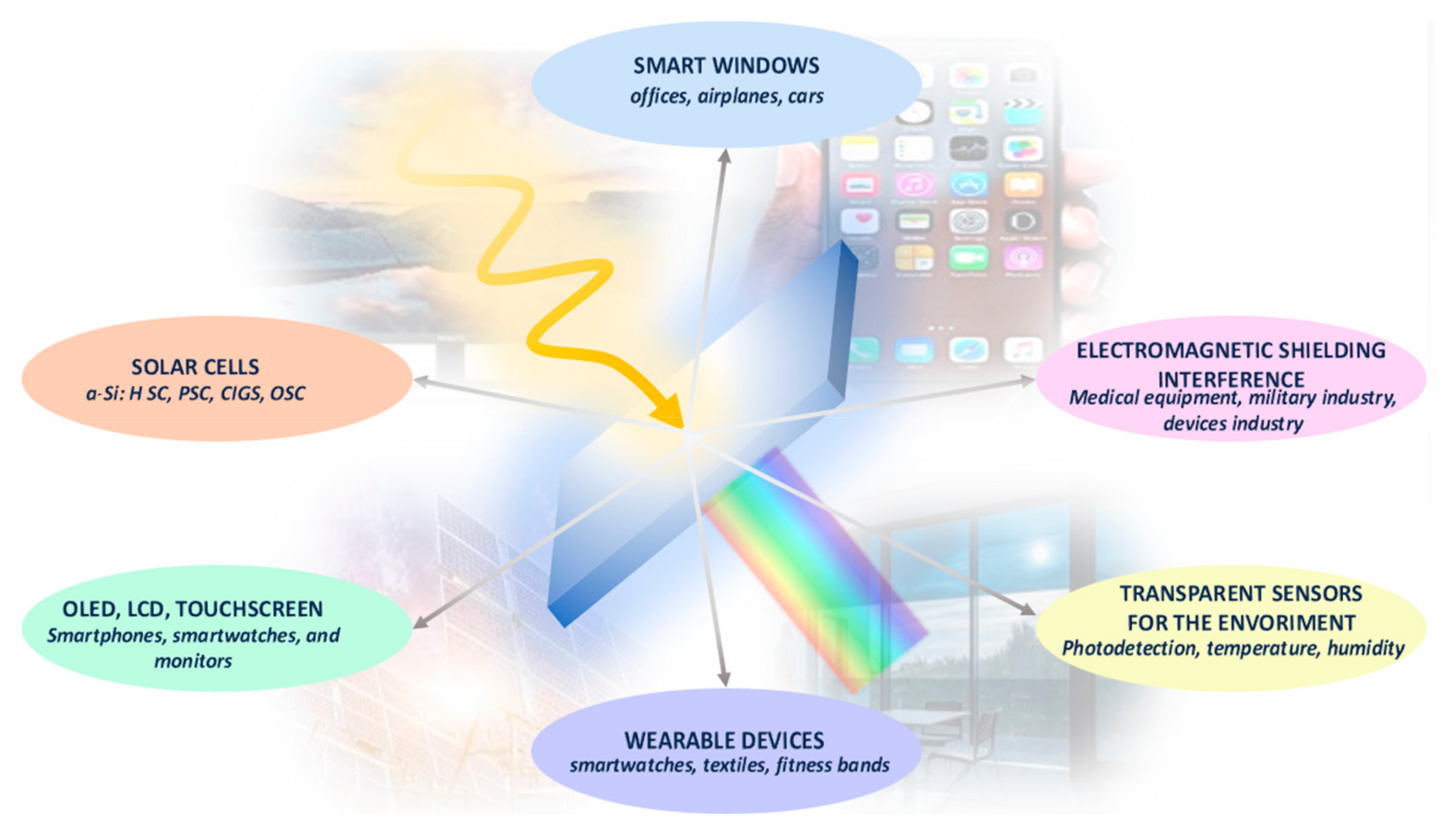
1. Introduction
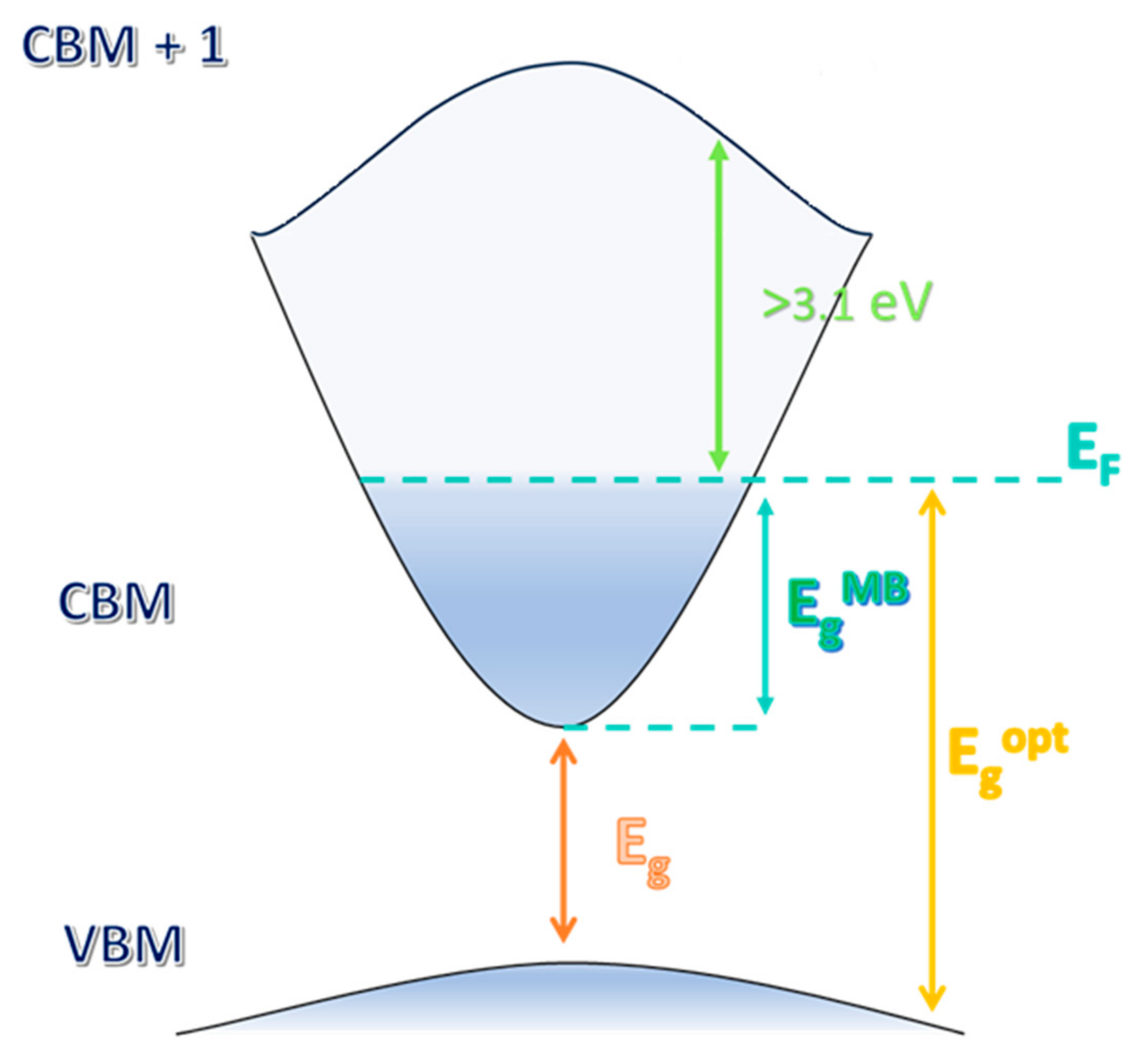
2. Optical and Electrical Properties

3. Indium Tin Oxide (ITO): Properties and Applications
4. Fluorine-Doped Tin Oxide (FTO): Properties and Applications
5. Aluminum-Doped Zinc Oxide (AZO): Properties and Applications
Towards Large-Area Deposition of Al:ZnO as Transparent Conducting Oxide (TCO)
6. Other TCOs
7. Conclusions
Author Contributions
Funding
Conflicts of Interest
References
- Flickyngerova, S.; Shtereva, K.; Stenova, V.; Hasko, D.; Novotny, I.; Tvarozek, V.; Sutta, P.; Vavrinsky, E. Structural and optical properties of sputtered ZnO thin films. Appl. Surf. Sci. 2008, 254, 3643–3647. [Google Scholar] [CrossRef]
- Lewis, B.G.; Paine, D.C. Applications and Processing of Transparent Conducting Oxides Large-Scale Manufacturing of ITO Thin-Film Coatings. MRS Bull. 2000, 25, 22–27. [Google Scholar] [CrossRef]
- Ellmer, K. Past achievements and future challenges in the development of optically transparent electrodes. Nat. Photonics 2012, 6, 809–817. [Google Scholar] [CrossRef]
- Minami, T. New n-Type Transparent Conducting Oxides. MRS Bull. 2000, 25, 38–44. [Google Scholar] [CrossRef]
- Lee, W.W.; Seo, Y.H.; Park, M.; Shin, Y.J.; Kwon, S.J.; Jeon, Y.; Cho, E.S. Development of transparent AZO-Ag-AZO electrodes using Xenon flash lamp annealing and application of transparent OLED. Appl. Surf. Sci. 2025, 684, 161861. [Google Scholar] [CrossRef]
- Datta, R.S.; Datta, R.S.; Syed, N.; Zavabeti, A.; Jannat, A.; Mohiuddin, M.; Rokunuzzaman, M.; Zhang, B.Y.; Rahman, M.A.; Atkin, P.; et al. Flexible two-dimensional indium tin oxide fabricated using a liquid metal printing technique. Nat. Electron. 2020, 3, 51–58. [Google Scholar] [CrossRef]
- Jayathilake, S.; Peiris, T.A.N. Overview on Transparent Conducting Oxides and State of the Art of Low-Cost Doped ZnO Systems. SF J. Mater. Chem. Eng. 2018, 1, 1004. [Google Scholar]
- Afre, R.A.; Sharma, N.; Sharon, M.; Sharon, M. Transparent conducting oxide films for various applications: A review. Inst. Probl. Mech. Eng. 2018, 53, 79–89. [Google Scholar] [CrossRef]
- Marinova, V.; Petrov, S.; Petrova, D.; Napoleonov, B.; Chau, N.H.M.; Lan, Y.P.; Strijkova, V.; Hsu, K.Y.; Dimitrov, D.; Lin, S.H. Effect of transparent conductive layers on the functionality of liquid crystal devices: Comparison of AZO, FTO and ITO. Opt. Mater. X 2024, 22, 100330. [Google Scholar] [CrossRef]
- Rezaie, M.N.; Manavizadeh, N.; Nadimi, E.; Boroumand, F.A. Quality enhancement of AZO thin films at various thicknesses by introducing ITO buffer layer. J. Mater. Sci. Mater. Electron. 2017, 28, 9328–9337. [Google Scholar] [CrossRef]
- Chen, T.L.; Ghosh, D.S.; Krautz, D.; Cheylan, S.; Pruneri, V. Highly stable Al-doped ZnO transparent conductors using an oxidized ultrathin metal capping layer at its percolation thickness. Appl. Phys. Lett. 2011, 99, 093302. [Google Scholar] [CrossRef]
- Sharma, M.; Chaudhary, D.; Dwivedi, N.; Sudhakar, S.; Kumar, S. Simulating the Role of TCO Materials, their Surface Texturing and Band Gap of Amorphous Silicon Layers on the Efficiency of Amorphous Silicon Thin Film Solar Cells. Silicon 2017, 9, 59–68. [Google Scholar] [CrossRef]
- Wen, L.; Sahu, B.B.; Kim, H.R.; Han, J.G. Study on the electrical, optical, structural, and morphological properties of highly transparent and conductive AZO thin films prepared near room temperature. Appl. Surf. Sci. 2019, 473, 649–656. [Google Scholar] [CrossRef]
- Habis, C.; Zaraket, J.; Aillerie, M. Transparent Conductive Oxides. Part I. General Review of Structural, Electrical and Optical Properties of TCOs Related to the Growth Techniques, Materials and Dopants. DDF 2022, 417, 243–256. [Google Scholar] [CrossRef]
- Gordon, R.G. Criteria for Choosing Transparent Conductors. MRS Bull. 2000, 25, 52–57. [Google Scholar] [CrossRef]
- Wang, Z.; Chen, C.; Wu, K.; Chong, H.; Ye, H. Transparent Conductive Oxides and Their Applications in Near Infrared Plasmonics. Phys. Status Solidi A 2019, 216, 1700794. [Google Scholar] [CrossRef]
- Castañeda, L. Review of Con-ducting Oxides Semiconductors in Thin Solid Films. Biomed. J. Sci. Tech. Res. 2022, 41, 32261–32270. [Google Scholar] [CrossRef]
- Zhang, L.; Zhou, Y.; Guo, L.; Zhao, W.; Barnes, A.; Zhang, H.T.; Eaton, C.; Zheng, Y.; Brahlek, M.; Haneef, H.F.; et al. Correlated metals as transparent conductors. Nat. Mater. 2016, 15, 204–210. [Google Scholar] [CrossRef] [PubMed]
- Singh, J.; Bhardwaj, P.; Kumar, R.; Verma, V. Progress in Developing Highly Efficient P-Type TCOs for Transparent Electronics: A Comprehensive Review; Springer: Berlin/Heidelberg, Germany, 2024. [Google Scholar] [CrossRef]
- y Díaz, E.C.; Camacho, J.M.; Duarte-Moller, A.; Castro-Rodríguez, R.; Bartolo-Pérez, P. Influence of the oxygen pressure on the physical properties of the pulsed-laser deposited Te doped SnO2 thin films. J. Alloys Compd. 2010, 508, 342–347. [Google Scholar] [CrossRef]
- Ellmer, K.; Klein, A. ZnO and Its Applications. In Transparent Conductive Zinc Oxide: Basics and Applications in Thin Film Solar Cells; Springer: Berlin/Heidelberg, Germany, 2008; pp. 1–33. [Google Scholar]
- Rozati, S.M.; Ziabari, S.A.M. A review of various single layer, bilayer, and multilayer TCO materials and their applications. Mater. Chem. Phys. 2022, 292, 126789. [Google Scholar] [CrossRef]
- Hosono, H.; Ueda, K. Transparent conductive oxides. In Springer Handbooks; Springer: Berlin/Heidelberg, Germany, 2017; p. 1. [Google Scholar] [CrossRef]
- Medvedeva, J.E.; Hettiarachchi, C.L. Tuning the properties of complex transparent conducting oxides: Role of crystal symmetry, chemical composition, and carrier generation. Phys. Rev. B—Condens. Matter Mater. Phys. 2010, 81, 125116. [Google Scholar] [CrossRef]
- Dixon, S.C.; Scanlon, D.O.; Carmalt, C.J.; Parkin, I.P. N-Type doped transparent conducting binary oxides: An overview. J. Mater. Chem. C 2016, 4, 6946–6961. [Google Scholar] [CrossRef]
- Ellmer, K.; Mientus, R. Carrier transport in polycrystalline transparent conductive oxides: A comparative study of zinc oxide and indium oxide. Thin Solid Films 2008, 516, 4620–4627. [Google Scholar] [CrossRef]
- Ghosh, S.; Basak, D. Correlation between Hall Mobility and Optical Mobility in Aluminum-Doped ZnO Films via Boundary Scatterings and Estimation of Donor Compensation Ratio. Phys. Status Solidi B Basic Res. 2020, 257, 1900682. [Google Scholar] [CrossRef]
- de Andrés, A.; Jiménez-Villacorta, F.; Prieto, C. Part I Electrical Conductive Materials: General Aspects. In Transparent Conductive Materials: Materials, Synthesis, Characterization, Applications; Wiley: Hoboken, NJ, USA, 2018; ISBN 978-3-527-80461-0. [Google Scholar]
- Haacke, G. New figure of merit for transparent conductors. J. Appl. Phys. 1976, 47, 4086–4089. [Google Scholar] [CrossRef]
- Cisneros-Contreras, I.R.; Muñoz-Rosas, A.L.; Rodríguez-Gómez, A. Resolution improvement in Haacke’s figure of merit for transparent conductive films. Results Phys. 2019, 15, 102695. [Google Scholar] [CrossRef]
- Mendez-Gamboa, J.A.; Castro-Rodriguez, R.; Perez-Quintana, I.V.; Medina-Esquivel, R.A.; Martel-Arbelo, A. A figure of merit to evaluate transparent conductor oxides for solar cells using photonic flux density. Thin Solid Films 2016, 599, 14–18. [Google Scholar] [CrossRef]
- Ravichandran, S.; Sahadevan, J.; Sivaprakash, P.; Sagadevan, S.; Kim, I.; Tighezza, A.M.; Amanat Ali, A.; Muthu, E.S. Synthesis and physicochemical properties of graphene incorporated indium tin oxide nanocomposites for optoelectronic device applications. Mater. Sci. Eng. B 2024, 301, 117199. [Google Scholar] [CrossRef]
- Jiao, X.; Li, S.; Lv, Z.; Jiao, H.; He, J.; Song, J. Advances of indium tin oxide in catalysis and cell. Mater. Today Commun. 2025, 44, 112058. [Google Scholar] [CrossRef]
- Eberst, A.; Xu, B.; Bittkau, K.; Duan, W.; Lambertz, A.; Meise, A.; Heggen, M.; Dunin-Borkowski, R.E.; Rau, U.; Ding, K. Deeper Insight into the Mechanisms Behind Sputter Damage in Silicon Solar Cells Based on the Example of Nanocrystalline Silicon Carbide. Adv. Phys. Res. 2024, 3, 2400036. [Google Scholar] [CrossRef]
- Du, D.; Liang, J.; Shen, W. Optimized optical and electrical properties for silicon heterojunction solar cells with an indium tin oxide buffer layer. Sol. Energy Mater. Sol. Cells 2025, 286, 113595. [Google Scholar] [CrossRef]
- Li, W.; Liu, X.; Zhang, J.; Wang, H.; Yuan, C.; Lin, S.; Chen, C.; Shen, C.; Tang, J.; Li, J.; et al. Reactive Plasma Deposition of ITO as an Efficient Buffer Layer for Inverted Perovskite Solar Cells. Adv. Mater. 2025, 37, e2417094. [Google Scholar] [CrossRef] [PubMed]
- Smirnov, Y.; Repecaud, P.A.; Tutsch, L.; Florea, I.; Zanoni, K.P.S.; Paliwal, A.; Bolink, H.J.; Cabarrocas, P.R.; Bivour, M.; Masis, M.M. Wafer-scale pulsed laser deposition of ITO for solar cells: Reduced damage vs. interfacial resistance. Mater. Adv. 2022, 3, 3469–3478. [Google Scholar] [CrossRef]
- Zanoni, K.P.S.; Paliwal, A.; Hernández-Fenollosa, M.A.; Repecaud, P.A.; Morales-Masis, M.; Bolink, H.J. ITO Top-Electrodes via Industrial-Scale PLD for Efficient Buffer-Layer-Free Semitransparent Perovskite Solar Cells. Adv. Mater. Technol. 2022, 7, 2101747. [Google Scholar] [CrossRef]
- Chen, C.; Wang, L.; Xia, W.; Qiu, K.; Guo, C.; Gan, Z.; Zhou, J.; Sun, Y.; Liu, D.; Li, W.; et al. Molecular interaction induced dual fibrils towards organic solar cells with certified efficiency over 20%. Nat. Commun. 2024, 15, 6865. [Google Scholar] [CrossRef]
- Huang, J.; Fu, J.; Yuan, B.; Xia, H.; Chen, T.; Lang, Y.; Liu, H.; Ren, Z.; Liang, Q.; Liu, K. 19.5% Inverted organic photovoltaic with record long-lifetime via multifunctional interface engineering featuring radical scavenger. Nat. Commun. 2024, 15, 10565. [Google Scholar] [CrossRef]
- Basu, R.; Gumpert, F.; Lohbreier, J.; Morin, P.O.; Vohra, V.; Liu, Y.; Zhou, Y.; Brabec, C.J.; Egelhaaf, H.J.; Distler, A. Large-area organic photovoltaic modules with 14.5% certified world record efficiency. Joule 2024, 8, 970–978. [Google Scholar] [CrossRef]
- Patel, J.; Sharme, R.K.; Quijada, M.A.; Rana, M.M. A Review of Transparent Conducting Films (TCFs): Prospective ITO and AZO Deposition Methods and Applications. Nanomaterials 2024, 14, 2013. [Google Scholar] [CrossRef]
- Liu, S.; Xu, X.; Jiang, J. Flexible transparent ITO thin film with high conductivity and high-temperature resistance. Ceram. Int. 2024, 50, 47649–47654. [Google Scholar] [CrossRef]
- Leterrier, Y.; Medico, L.; Demarco, F.; Manson, J.-A.E.; Betz, U.; Escola, M.F.; Olsson, M.K.; Atamny, F. Mechanical integrity of transparent conductive oxide films for flexible polymer-based displays. Thin Solid Films 2004, 460, 156–166. [Google Scholar] [CrossRef]
- Wu, C.C. Highly flexible touch screen panel fabricated with silver-inserted transparent ITO triple-layer structures. RSC Adv. 2018, 8, 11862–11870. [Google Scholar] [CrossRef]
- Erdogan, N.; Erden, F.; Astarlioglu, A.T.; Ozdemir, M.; Ozbay, S.; Aygun, G.; Ozyuzer, L. ITO/Au/ITO multilayer thin films on transparent polycarbonate with enhanced EMI shielding properties. Curr. Appl. Phys. 2020, 20, 489–497. [Google Scholar] [CrossRef]
- Feng, B.; Yang, T.; Zhu, S.; Yue, Y.; Zhou, B.; Yao, Z.; Liu, C.; Han, J. Flexible, highly transparent, and conductive ITO/Ag/ITO film with double symmetric structure for electrical heater and broadband electromagnetic interference shielding. Chem. Eng. J. 2025, 516, 164233. [Google Scholar] [CrossRef]
- Huang, X.; Yu, Z.; Huang, S.; Zhang, Q.; Li, D.; Luo, Y.; Meng, Q. Preparation of fluorine-doped tin oxide (SnO2:F) film on polyethylene terephthalate (PET) substrate. Mater. Lett. 2010, 64, 1701–1703. [Google Scholar] [CrossRef]
- Das, S.; Jayaraman, V. SnO2: A comprehensive review on structures and gas sensors. Prog. Mater. Sci. 2014, 66, 112–255. [Google Scholar] [CrossRef]
- Banyamin, Z.Y.; Kelly, P.J.; West, G.; Boardman, J. Electrical and optical properties of fluorine doped tin oxide thin films prepared by magnetron sputtering. Coatings 2014, 4, 732–746. [Google Scholar] [CrossRef]
- Ramaiah, K.S.; Raja, V.S. Structural and electrical properties of fluorine doped tin oxide films prepared by spray-pyrolysis technique. Appl. Surf. Sci. 2006, 253, 1451–1458. [Google Scholar] [CrossRef]
- Shi, X.H.; Xu, K.J. Properties of fluorine-doped tin oxide films prepared by an improved sol-gel process. Mater. Sci. Semicond. Process. 2017, 58, 1–7. [Google Scholar] [CrossRef]
- Zhu, B.L.; Peng, H.; Tao, Y.; Wu, J.; Shi, X.W. Highly transparent conductive F-doped SnO2 films prepared on polymer substrate by radio frequency reactive magnetron sputtering. Thin Solid Films 2022, 756, 139360. [Google Scholar] [CrossRef]
- Kim, J. Texture changes of fluorine-doped tin oxide (FTO) coatings using ultrasonic spray pyrolysis. Ceram. Int. 2024, 50, 38342–38349. [Google Scholar] [CrossRef]
- Heffner, H.; Soldera, M.; Lasagni, A.F. Optical Enhancement of Fluorine-Doped Tin Oxide Thin Films using Infrared Picosecond Direct Laser Interference Patterning. Adv. Eng. Mater. 2022, 24, 2200266. [Google Scholar] [CrossRef]
- Ouerfelli, J.; Djobo, S.O.; Bernède, J.C.; Cattin, L.; Morsli, M.; Berredjem, Y. Organic light emitting diodes using fluorine doped tin oxide thin films, deposited by chemical spray pyrolysis, as anode. Mater. Chem. Phys. 2008, 112, 198–201. [Google Scholar] [CrossRef]
- Yadav, A.A.; Masumdar, E.U.; Moholkar, A.V.; Neumann-Spallart, M.; Rajpure, K.Y.; Bhosale, C.H. Electrical, structural and optical properties of SnO2:F thin films: Effect of the substrate temperature. J. Alloys Compd. 2009, 488, 350–355. [Google Scholar] [CrossRef]
- Way, A.; Luke, J.; Evans, A.D.; Li, Z.; Kim, J.S.; Durrant, J.R.; Lee, H.K.H.; Tsoi, W.C. Fluorine doped tin oxide as an alternative of indium tin oxide for bottom electrode of semi-transparent organic photovoltaic devices. AIP Adv. 2019, 9, 085220. [Google Scholar] [CrossRef]
- Deva, K.; Valanarasu, S.; Capelle, A.; Nar, S.; Karim, W.; Stolz, A.; Aspe, B.; Semmar, N. Nanostructured Oxide (SnO2, FTO) Thin Films for Energy Harvesting: A Significant Increase in Thermoelectric Power at Low Temperature. Micromachines 2024, 15, 188. [Google Scholar] [CrossRef]
- Aouaj, M.A.; Diaz, R.; Belayachi, A.; Rueda, F.; Abd-Lefdil, M. Comparative study of ITO and FTO thin films grown by spray pyrolysis. Mater. Res. Bull. 2009, 44, 1458–1461. [Google Scholar] [CrossRef]
- Wang, Y.; Wu, Y.; Qin, Y.; Zhang, Z.; Shi, C.; Zhang, Q.; Li, C.; Xia, X.; Sun, S.; Chen, L. Large-area SnO2: F thin films by offline APCVD. Mater. Res. Bull. 2011, 46, 1262–1265. [Google Scholar] [CrossRef]
- Kim, H.; Auyeung, R.C.Y.; Piqué, A. F-doped SnO2 thin films grown on flexible substrates at low temperatures by pulsed laser deposition. Thin Solid Films 2011, 520, 497–500. [Google Scholar] [CrossRef]
- Muthukumar, A.; Rey, G.; Giusti, G.; Consonni, V.; Appert, E.; Roussel, H.; Dakshnamoorthy, A.; Bellet, D. Fluorine doped tin oxide (FTO) thin film as transparent conductive oxide (TCO) for photovoltaic applications. AIP Conf. Proc. 2013, 1512, 710–711. [Google Scholar] [CrossRef]
- AL-Arique, H.Q.N.M.; AL-Qadasy, S.S.S.; Kaawash, N.M.S.; Chishty, S.Q.; Bogle, K.A. Study the characterization of ZnO and AZO films prepared by spray pyrolysis and the effect of annealing temperature. Opt. Mater. 2024, 150, 115261. [Google Scholar] [CrossRef]
- Dutta, S.; Chattopadhyay, S.; Sarkar, A.; Chakrabarti, M.; Sanyal, D.; Jana, D. Role of defects in tailoring structural, electrical and optical properties of ZnO. Prog. Mater. Sci. 2009, 54, 89–136. [Google Scholar] [CrossRef]
- Bingel, A.; Stenzel, O.; Naujok, P.; Müller, R.; Shestaeva, S.; Steglich, M.; Schulz, U.; Kaiser, N.; Tünnermann, A. AZO/Ag/AZO transparent conductive films: Correlation between the structural, electrical, and optical properties and development of an optical model. Opt. Mater. Express 2016, 6, 3217. [Google Scholar] [CrossRef]
- Girtan, M.; Hrostea, L.; Boclinca, M.; Negulescu, B. Study of oxide/metal/oxide thin films for transparent electronics and solar cells applications by spectroscopic ellipsometry. AIMS Mater. Sci. 2017, 4, 594–613. [Google Scholar] [CrossRef]
- Amakali, T.; Daniel, L.S.; Uahengo, V.; Dzade, N.Y.; de Leeuw, N.H. Structural and optical properties of ZnO thin films prepared by molecular precursor and sol–gel methods. Crystals 2020, 10, 132. [Google Scholar] [CrossRef]
- Dong, B.Z.; Fang, G.J.; Wang, J.F.; Guan, W.J.; Zhao, X.Z. Effect of thickness on structural, electrical, and optical properties of ZnO: Al films deposited by pulsed laser deposition. J. Appl. Phys. 2007, 101, 033713. [Google Scholar] [CrossRef]
- Sharmin, A.; Tabassum, S.; Bashar, M.S.; Mahmood, Z.H. Depositions and characterization of sol–gel processed Al-doped ZnO (AZO) as transparent conducting oxide (TCO) for solar cell application. J. Theor. Appl. Phys. 2019, 13, 123–132. [Google Scholar] [CrossRef]
- Zhang, H.; Wang, Y.; Zhao, W.; Zou, M.; Chen, Y.; Yang, L.; Xu, L.; Wu, H.; Cao, A. MOF-Derived ZnO Nanoparticles Covered by N-Doped Carbon Layers and Hybridized on Carbon Nanotubes for Lithium-Ion Battery Anodes. ACS Appl. Mater. Interfaces 2017, 9, 37813–37822. [Google Scholar] [CrossRef]
- Raj, I.L.P.; Valanarasu, S.; Hariprasad, K.; Ponraj, J.S.; Chidhambaram, N.; Ganesh, V.; Ali, H.E.; Khairy, Y. Enhancement of optoelectronic parameters of Nd-doped ZnO nanowires for photodetector applications. Opt. Mater. 2020, 109, 110396. [Google Scholar] [CrossRef]
- Galstyan, V.; Comini, E.; Baratto, C.; Faglia, G.; Sberveglieri, G. Nanostructured ZnO chemical gas sensors. Ceram. Int. 2015, 41 Pt B, 14239–14244. [Google Scholar] [CrossRef]
- Locovei, C.; Coman, D.; Radu, A.; Ion, L.; Antohe, V.A.; Vasile, N.; Dumitru, A.; Iftimie, S.; Antohe, S. Physical properties of Cu and Dy co-doped ZnO thin films prepared by radio frequency magnetron sputtering for hybrid organic/inorganic electronic devices. Thin Solid Films 2019, 685, 379–384. [Google Scholar] [CrossRef]
- Vasile, N.; Iftimie, S.; Acsente, T.; Locovei, C.; Călugăr, A.I.; Radu, A.; Ion, L.; Antohe, V.A.; Manica, D.; Toma, O. Physical properties of indium zinc oxide and aluminium zinc oxide thin films deposited by radio-frequency magnetron sputtering. Mater. Res. Express 2019, 6, 126447. [Google Scholar] [CrossRef]
- Nunes, P.; Fortunato, E.; Martins, R. Influence of the post-treatment on the properties of ZnO thin films. Thin Solid Films 2001, 383, 277–280. [Google Scholar] [CrossRef]
- Ellmer, K. Resistivity of Polycrystalline Zinc Oxide Films: Current Status and Physical Limit. J. Phys. D Appl. Phys. 2001, 34, 3097. [Google Scholar] [CrossRef]
- Lin, M.L.; Huang, J.M.; Ku, C.S.; Lin, C.M.; Lee, H.Y.; Juang, J.Y. High mobility transparent conductive Al-doped ZnO thin films by atomic layer deposition. J. Alloys Compd. 2017, 727, 565–571. [Google Scholar] [CrossRef]
- Akdaǧ, A.; Budak, H.F.; Yılmaz, M.; Efe, A.; Büyükaydın, M.; Can, M.; Turgut, G.; Sönmez, E. Structural and Morphological Properties of Al doped ZnO Nanoparticles. In Journal of Physics Conference Series; Institute of Physics Publishing: Bristol, UK, 2016. [Google Scholar] [CrossRef]
- Stroescu, H.; Nicolescu, M.; Mitrea, D.; Tenea, E.; Atkinson, I.; Anastasescu, M.; Calderon-Moreno, L.M.; Gartner, M. Effect of Al Incorporation on the Structural and Optical Properties of Sol–Gel AZO Thin Films. Materials 2023, 16, 3329. [Google Scholar] [CrossRef] [PubMed]
- Pat, S.; Mohammadigharehbagh, R.; Özen, S.; Şenay, V.; Yudar, H.H.; Korkmaz, Ş. The Al doping effect on the surface, optical, electrical and nanomechanical properties of the ZnO and AZO thin films prepared by RF sputtering technique. Vacuum 2017, 141, 210–215. [Google Scholar] [CrossRef]
- Chen, W.J.; Liu, W.L.; Hsieh, S.H.; Hsu, Y.G. Synthesis of ZnO:Al transparent conductive thin films using sol-gel method. Procedia Eng. 2012, 36, 54–61. [Google Scholar] [CrossRef]
- Kaid, M.A.; Ashour, A. Preparation of ZnO-doped Al films by spray pyrolysis technique. Appl. Surf. Sci. 2007, 253, 3029–3033. [Google Scholar] [CrossRef]
- Ma, J.; Ji, F.; Zhang, D.-H.; Ma, H.-l.; Li, S.-Y. Optical and Electronic Properties of Transparent Conducting ZnO and ZnO:Alms Prepared by Evaporating Method. Thin Solid Films 1999, 357, 98–101. [Google Scholar] [CrossRef]
- Shirahata, T.; Kawaharamura, T.; Fujita, S.; Orita, H. Transparent conductive zinc-oxide-based films grown at low temperature by mist chemical vapor deposition. Thin Solid Films 2015, 597, 30–38. [Google Scholar] [CrossRef]
- Gu, X.Q.; Zhu, L.P.; Cao, L.; Ye, Z.Z.; He, H.P.; Chu, P.K. Optical and electrical properties of ZnO:Al thin films synthesized by low-pressure pulsed laser deposition. Mater. Sci. Semicond. Process. 2011, 14, 48–51. [Google Scholar] [CrossRef]
- Challali, F.; Mendilb, D.; Touamb, T.; Chauveaua, T.; Bockeléea, V.; Sancheza, A.G.; Chelouched, A.; Besland, M.P. Effect of RF sputtering power and vacuum annealing on the properties of AZO thin films prepared from ceramic target in confocal configuration. Mater. Sci. Semicond. Process. 2020, 118, 105217. [Google Scholar] [CrossRef]
- Lennon, C.; Tapia, R.B.; Kodama, R.; Chang, Y.; Sivananthan, S.; Deshpande, M. Effects of annealing in a partially reducing atmosphere on sputtered Al-Doped ZnO thin films. J. Electron. Mater. 2009, 38, 1568–1573. [Google Scholar] [CrossRef]
- Fang, G.J.; Li, D.J.; Yao, B.L. Effect of vacuum annealing on the properties of transparent conductive AZO thin films prepared by DC magnetron sputtering. Phys. Status Solidi A Appl. Res. 2002, 193, 139–152. [Google Scholar] [CrossRef]
- Chaves, M.; Ramosa, R.; Martins, E.; Rangela, E.C.; da Cruz, N.C.; Durranta, S.F.; Bortoleto, J.R.R. Al-doping and properties of AZO thin films grown at room temperature: Sputtering pressure effect. Mater. Res. 2019, 22, e20180665. [Google Scholar] [CrossRef]
- Girtan, M.; Vlad, A.; Mallet, R.; Bodea, M.A.; Pedarnig, J.D.; Stanculescu, A.; Mardare, D.; Leontie, L.; Antohe, S. On the properties of aluminium doped zinc oxide thin films deposited on plastic substrates from ceramic targets. Appl. Surf. Sci. 2013, 274, 306–313. [Google Scholar] [CrossRef]
- Agura, H.; Suzuki, A.; Matsushita, T.; Aoki, T.; Okuda, M. Low resistivity transparent conducting Al-doped ZnO films prepared by pulsed laser deposition. Thin Solid Films 2003, 445, 263–267. [Google Scholar] [CrossRef]
- Ohta, H.; Orita, M.; Hirano, M.; Tanji, H.; Kawazoe, H.; Hosono, H. Highly electrically conductive indium-tin-oxide thin films epitaxially grown on yttria-stabilized zirconia (100) by pulsed-laser deposition. Appl. Phys. Lett. 2000, 76, 2740–2742. [Google Scholar] [CrossRef]
- Anyanwu, V.O.; Moodley, M.K. PLD of transparent and conductive AZO thin films. Ceram. Int. 2023, 49, 5311–5318. [Google Scholar] [CrossRef]
- Lee, J.C.; Dutta, V.; Yoo, J.; Yi, J.; Song, J.; Yoon, K.H. Superstrate p-i-n a-Si:H solar cells on textured ZnO:Al front transparent conduction oxide. Superlattices Microstruct. 2007, 42, 369–374. [Google Scholar] [CrossRef]
- Kim, H.; Lee, K.T.; Zhao, C.; Guo, L.J.; Kanicki, J. Top illuminated organic photodetectors with dielectric/metal/dielectric transparent anode. Org. Electron. 2015, 20, 103–111. [Google Scholar] [CrossRef]
- Zhang, Y.; Zheng, H.; Yang, P.; Yu, S. Synthesis and analysis of optical, electrical and electromagnetic shielding properties of Ag/AZO films. J. Mater. Sci. Mater. Electron. 2025, 36, 443. [Google Scholar] [CrossRef]
- Jeong, J.K.; Yun, H.J.; Yang, S.D.; Eom, K.Y.; Chea, S.W.; Park, J.H.; Lee, H.D.; Lee, G.W. Investigation of atomic-layer-deposited Al-doped ZnO film for AZO/ZnO double-stacked active layer thin-film transistor application. Thin Solid Films 2017, 638, 89–95. [Google Scholar] [CrossRef]
- Shen, H.L.; Zhang, H.; Lu, L.F.; Jiang, F.; Yang, C. Preparation and properties of AZO thin films on different substrates. Prog. Nat. Sci. Mater. Int. 2010, 20, 44–48. [Google Scholar] [CrossRef]
- Di Mauro, A.; Farrugia, C.; Abela, S.; Refalo, P.; Grech, M.; Falqui, L.; Privitera, V.; Impellizzeri, G. Synthesis of ZnO/PMMA nanocomposite by low-temperature atomic layer deposition for possible photocatalysis applications. Mater. Sci. Semicond. Process. 2020, 118, 105214. [Google Scholar] [CrossRef]
- Badgujar, A.C.; Yadav, B.S.; Jha, G.K.; Dhage, S.R. Room Temperature Sputtered Aluminum-Doped ZnO Thin Film Transparent Electrode for Application in Solar Cells and for Low-Band-Gap Optoelectronic Devices. ACS Omega 2022, 7, 14203–14210. [Google Scholar] [CrossRef] [PubMed]
- Hossain, M.A.; Patwary, M.A.M.; Rahman, M.M.; Ohtsu, Y. Properties of AZO thin films prepared by stationary and rotating RF magnetized plasma sputtering source. AIP Adv. 2022, 12, 015224. [Google Scholar] [CrossRef]
- Challali, F.; Touam, T.; Bockelée, V.; Chauveau, T.; Chelouche, A.; Stephant, N.; Hamon, J.; Besland, M.P. Comprehensive characterization of Al-doped ZnO thin films deposited in confocal radio frequency magnetron co-sputtering. Thin Solid Films 2023, 780, 139947. [Google Scholar] [CrossRef]
- Szyszka, B.; Sittinger, V.; Jiang, X.; Hong, R.J.; Werner, W.; Pflug, A.; Ruske, M.; Lopp, A. Transparent and conductive ZnO:Al films deposited by large area reactive magnetron sputtering. Thin Solid Films 2003, 442, 179–183. [Google Scholar] [CrossRef]
- Dhage, S.R.; Badgujar, A.C. Transparent conducting Al:ZnO thin films on large area by efficient cylindrical rotating DC magnetron sputtering. J. Alloys Compd. 2018, 763, 504–511. [Google Scholar] [CrossRef]
- Guillen, C.; Herrero, J. Structure, optical and electrical properties of Al:ZnO thin films deposited by DC sputtering at room temperature on glass and plastic substrates. Phys. Status Solidi A Appl. Mater. Sci. 2009, 206, 1531–1536. [Google Scholar] [CrossRef]
- Salim, K.; Medles, M.; Nakrela, A.; Miloua, R.; Bouzidi, A.; Desfeux, R. Enhancement of optical and electrical properties of spray pyrolysed ZnO thin films obtained from nitrate chemical by Al-Sn co-doping. Optik 2020, 210, 164504. [Google Scholar] [CrossRef]
- Tönbül, B.; Can, H.A.; Öztürk, T.; Akyıldız, H. Solution processed aluminum-doped ZnO thin films for transparent heater applications. Mater. Sci. Semicond. Process. 2021, 127, 105735. [Google Scholar] [CrossRef]
- Chavan, G.T.; Kim, Y.; Khokhar, M.Q.; Hussain, S.Q.; Cho, E.C.; Yi, J.; Ahmad, Z.; Rosaiah, P.; Jeon, C.W. A Brief Review of Transparent Conducting Oxides (TCO): The Influence of Different Deposition Techniques on the Efficiency of Solar Cells. Nanomaterials 2023, 13, 1226. [Google Scholar] [CrossRef]
- Choi, Y.J.; Gong, S.C.; Johnson, D.C.; Golledge, S.; Yeom, G.Y.; Park, H.H. Characteristics of the electromagnetic interference shielding effectiveness of Al-doped ZnO thin films deposited by atomic layer deposition. Appl. Surf. Sci. 2013, 269, 92–97. [Google Scholar] [CrossRef]
- Van Toan, N.; Tuoi, T.T.K.; Inomata, N.; Toda, M.; Ono, T. Aluminum doped zinc oxide deposited by atomic layer deposition and its applications to micro/nano devices. Sci. Rep. 2021, 11, 1204. [Google Scholar] [CrossRef]
- Swatowska, B.; Powroznik, W.; Czternastek, H.; Lewinska, G.; Stapinski, T.; Pietruszka, R.; Witkowski, B.S.; Godlewski, M. Application properties of ZnO and AZO thin films obtained by the ALD method. Energies 2021, 14, 6271. [Google Scholar] [CrossRef]
- Dugrenil, B.; Séguy, I.; Lee, H.Y.; Camps, T.; Lin, Y.-C.; Doucet, J.B.; Chiu, Y.-S.; Salvagnac, L.; Bedel-Pereira, E.; Ternisien, M.; et al. AZO electrodes deposited by atomic layer deposition for OLED fabrication. In Organic Photonics VI; SPIE: Brussels, Belgium, 2014; p. 91371D. [Google Scholar] [CrossRef]
- Baek, S.; Lee, J.C.; Lee, Y.J.; Iftiquar, S.S.; Kim, Y.; Park, J.; Yi, J. Interface modification effect between p-type a-SIC:H and ZnO:Al in p-i-n amorphous silicon solar cells. Nanoscale Res. Lett. 2012, 7, 81. [Google Scholar] [CrossRef]
- Yu, J.; Han, W.; Suleiman, A.A.; Han, S.; Miao, N.; Ling, F.C.C. Recent Advances on Pulsed Laser Deposition of Large-Scale Thin Films. Small Methods 2024, 8, e2301282. [Google Scholar] [CrossRef]
- Lorenz, M. Pulsed Laser Deposition of ZnO-Based Thin Films. In Transparent Conductive Zinc Oxide: Basics and Applications in Thin Film Solar Cells; Springer: Berlin/Heidelberg, Germany, 2008; pp. 303–357. [Google Scholar]
- Vakulov, Z.; Khakhulin, D.; Zamburg, E.; Mikhaylichenko, A.; Smirnov, V.A.; Tominov, R.; Klimin, V.S.; Ageev, O.A. Towards scalable large-area pulsed laser deposition. Materials 2021, 14, 4854. [Google Scholar] [CrossRef]
- Reinders, J.W.C.; Bolding, J.; Roldán-Carmona, C.; Ventosinos, F.; Paliwal, A.; Gil-Escrig, L.; Palazon, F.; Sessolo, M.; Zanoni, K.P.S.; Bolink, H.J. Room Temperature Pulsed Laser Deposition of Aluminum Zinc Oxide (AZO): Enabling Scalable Indium-Free Transparent Conductive Oxides. Adv. Funct. Mater. 2025, 35, 2418069. [Google Scholar] [CrossRef]
- Besleaga, C.; Ion, L.; Ghenescu, V.; Socol, G.; Radu, A.; Arghir, I.; Florica, C.; Antohe, S. Transparent indium zinc oxide thin films used in photovoltaic cells based on polymer blends. Thin Solid Films 2012, 520, 6803–6806. [Google Scholar] [CrossRef]
- Silva-Lopez, H.E.; Marcelino, B.S.; Guillen-Cervantes, A.; Zelaya-Angel, O.; Ramirez-Bon, R. Physical Properties of Sputtered Indium-doped ZnO Films Deposited on Flexible Transparent Substrates. Mater. Res. 2018, 21, e20180224. [Google Scholar] [CrossRef]
- Koida, T.; Kondo, M. High-mobility transparent conductive Zr-doped In2O3. Appl. Phys. Lett. 2006, 89, 082104. [Google Scholar] [CrossRef]
- Calnan, S.; Tiwari, A.N. High mobility transparent conducting oxides for thin film solar cells. Thin Solid Films 2010, 518, 1839–1849. [Google Scholar] [CrossRef]
- Morales-Masis, M.; Rucavado, E.; Monnard, R.; Barraud, L.; Holovský, J.; Despeisse, M.; Boccard, M.; Ballif, C. Highly conductive and broadband transparent Zr-doped In2O3 as front electrode for solar cells. IEEE J. Photovolt. 2018, 8, 1202–1207. [Google Scholar] [CrossRef]
- Oh, H.J.; Kim, Y.S.; Jeong, H.J.; Lee, S.; Park, J.S.; Park, J.S. Compositional tailoring of indium-free GZO layers via plasma-enhanced atomic layer deposition for highly stable IGZO/GZO TFT. J. Inf. Disp. 2024, 25, 295–303. [Google Scholar] [CrossRef]
- Zhang, Y.; Pan, Y. Investigation on Physical Properties of IGZO Thin Films under the Conditions of Mixing Oxygen and Argon. Coatings 2022, 12, 1425. [Google Scholar] [CrossRef]
- Kim, J.; Bang, S.; Lee, S.; Shin, S.; Joohyun Park, J.; Seo, H.; Jeon, H. A study on H2 plasma treatment effect on a-IGZO thin film transistor. J. Mater. Res. 2012, 27, 2318–2325. [Google Scholar] [CrossRef]
- Hwang, C.; Kim, T.; Jang, Y.; Lee, D.; Kim, H.D. Enhanced Optical and Electrical Properties of IGZO/Ag/IGZO for Solar Cell Application via Post-Rapid Thermal Annealing. Nanomaterials 2024, 14, 1841. [Google Scholar] [CrossRef]
- Yuan, Z.S.; Wu, C.C.; Tzou, W.C.; Yang, C.F.; Chen, Y.H. Investigation of high transparent and conductivity of IGZO/Ag/IGZO sandwich structures deposited by sputtering method. Vacuum 2019, 165, 305–310. [Google Scholar] [CrossRef]
- Ke, S.; Du, B.; Rao, Z.; Huang, C.; Lin, P.; Hu, Y.; Shu, L. Pulsed laser deposition of amorphous InGaZnO4 as an electron transport layer for perovskite solar cells. J. Adv. Dielectr. 2019, 9, 1950042. [Google Scholar] [CrossRef]
- Smirnov, Y.; Schmengler, L.; Kuik, R.; Repecaud, P.A.; Najafi, M.; Zhang, D.; Theelen, M.; Aydin, E.; Veenstra, S.; De Wolf, S.; et al. Scalable Pulsed Laser Deposition of Transparent Rear Electrode for Perovskite Solar Cells. Adv. Mater. Technol. 2021, 6, 2000856. [Google Scholar] [CrossRef]


| Deposition Method | ρ (Ω cm) | TVIS (%)/k | Scalability | Applications | Ref. |
|---|---|---|---|---|---|
| Magnetron Sputtering | 0.9 1 × 10⁻³ | 75.8 | 300 × 300 mm | Used as transparent electrode in CIGS solar cell (PCE—11.8%) | [101] |
| 5.75 × 10⁻⁴ (after annealing treatment) | 86 (after annealing treatment) | Large area glass substrate | - | [87] | |
| 3.6 × 10⁻⁴ | 86 | 100 mm glass substrate | - | [102] | |
| 3.9 × 10⁻³ (after annealing treatment) | 85 | 2.5 × 1.7 mm2 silicon and glass substrate | -/prepared as TCO. They reported a figure of merit of 43.6 × 10⁻⁴ sq.Ω−1 for a sample with 3.6 % Al content, after an annealing treatment. | [103] | |
| 4.07 × 10⁻⁴ | 84 | 300 mm × 300 mm glass substrate | - | [105] | |
| 2 × 10⁻³ | 90 | 12 × 40 mm2 on PET | - | [106] | |
| Spray Pyrolysis | 2.9 × 10⁻³ | 83 | 50 × 75 mm2 glass substrates | Heater applications | [108] |
| ALD | 6.24 × 10⁻⁴ | - | 4-inch glass wafer | OLED (Current density at 20 V—0.25 A/cm2) | [113]. |
| 6.33 × 10⁻³ | - | 4″ (100) Czochralski silicon wafer | - | [112] | |
| 5.876 × 10⁻⁴ | 85.93 | Silicon wafers and glass substrates | EMI (SE-1.1 dB for 121 nm undoped ZnO, and 6.5 dB for 131 nm Al-doped ZnO sample) | [110] | |
| PLD | 5.5 × 10⁻⁴ | 63.3 | Circular area of 500 cm2 | Employed in three different configurations of p-i-n PSC as superstrate (bottom illumination-PCE of 18.5%), semitransparent (bottom illumination-PCE of 17.2%), and semitransparent (top illumination-PCE of 18.9%-best performance) | [118] |
| ρ (Ω cm) | Rs (Ω/sq.) | TVIS (%) | A (%) | k | Deposition Method | Applications | Ref. | |
|---|---|---|---|---|---|---|---|---|
| ITO | 4.87 × 10⁻⁴ | 46.1% | 88.71% | - | 0.009 | PVD | SHJ (PCE-25.36%) | [35] |
| - | 60 Ω/sq. | - | Less than 5% | - | PLD | SHJ (PCE->22%) | [37] | |
| 4 × 10⁻⁴ | 25 Ω/sq. | More than 70% | Below 10% | - | PLD | Semitransparent PSC (PCE-18%) | [38] | |
| - | 6.4 Ω/sq. | 87.5% | - | - | Sputtering | TSPs | [45] | |
| - | 4.01 Ω/sq. | 87.4% | - | - | Sputtering | EMI (SE-36.5 dB) | [47] | |
| AZO | 1.94 × 10⁻² | - | >85% | - | - | Sol-gel | CIGS solar cell | [82] |
| 7.1 × 10⁻⁴ | - | 86.9% | - | - | Sputtering | - | [88] | |
| 1.3 × 10⁻³ | - | >85% | - | - | PLD | Electrode for plastic solar cell | [91] | |
| 8.54 × 10⁻⁵ | - | 88% | - | - | PLD | - | [92] | |
| 6.8 × 10⁻⁵ | - | 83% | - | - | PLD | - | [94] | |
| 1.5 × 10⁻⁵ | 4.95 Ω/sq. | 82.9% | - | - | magnetron sputtering | EMI (SE-27.1 Db) | [97] | |
| 10−4 | - | Above 90% | - | - | Magnetron Sputtering | - | [89] | |
| 2.8 × 10⁻³ | - | 80% | - | - | Magnetron Sputtering | - | [90] | |
| FTO | - | 10 Ω/sq. | 83% | - | - | APCVD | Tandem amorphous silicon (a-Si:H) tandem solar cell | [61] |
| 1.3 × 10⁻³ | 40 Ω/sq. | 89% | PLD | Transparent electrodes for flexible devices | [62] | |||
| 4.3 × 10⁻⁴ | - | 86% | Ultrasonic spray pyrolysis | - | [63] | |||
| Others TCO | ||||||||
| IZO | 1.8 × 10⁻⁴ | - | 80% | - | - | Rf magnetron sputtering | - | [120] |
| 4.8 × 10⁻⁴ | - | 80% | - | - | PLD | Electrodes in a polymer-based photovoltaic cell | [119] | |
| IZrO | - | 21 Ω/sq. | 80% | Less than 10% | - | PLD | Used as a rear electrode in semi-transparent PSC (High stabilized efficiency of 15.1%) | [130] |
| - | 25 Ω/sq. | 80% | Less than 10% | 0 | Rf sputtering | Used as front electrode in SHJ (PCE-23.4%) | [123] | |
| IGZO | - | 6 Ω/sq. | 85% | - | - | Rf sputtering | Solar cell (JSC-40 mA/cm) | [127] |
| 5 × 10⁻⁵ | 2.5 Ω/sq. | 89.5% | - | - | Rf magnetron sputtering | - | [128] | |
| - | - | - | - | - | PLD | PSC device (efficiency-15.11%) | [129] | |
Disclaimer/Publisher’s Note: The statements, opinions and data contained in all publications are solely those of the individual author(s) and contributor(s) and not of MDPI and/or the editor(s). MDPI and/or the editor(s) disclaim responsibility for any injury to people or property resulting from any ideas, methods, instructions or products referred to in the content. |
© 2025 by the authors. Licensee MDPI, Basel, Switzerland. This article is an open access article distributed under the terms and conditions of the Creative Commons Attribution (CC BY) license (https://creativecommons.org/licenses/by/4.0/).
Share and Cite
Bancu, E.I.; Ion, V.; Antohe, S.; Scarisoreanu, N.D. Towards AZO Thin Films for Electronic and Optoelectronic Large-Scale Applications. Crystals 2025, 15, 670. https://doi.org/10.3390/cryst15080670
Bancu EI, Ion V, Antohe S, Scarisoreanu ND. Towards AZO Thin Films for Electronic and Optoelectronic Large-Scale Applications. Crystals. 2025; 15(8):670. https://doi.org/10.3390/cryst15080670
Chicago/Turabian StyleBancu, Elena Isabela, Valentin Ion, Stefan Antohe, and Nicu Doinel Scarisoreanu. 2025. "Towards AZO Thin Films for Electronic and Optoelectronic Large-Scale Applications" Crystals 15, no. 8: 670. https://doi.org/10.3390/cryst15080670
APA StyleBancu, E. I., Ion, V., Antohe, S., & Scarisoreanu, N. D. (2025). Towards AZO Thin Films for Electronic and Optoelectronic Large-Scale Applications. Crystals, 15(8), 670. https://doi.org/10.3390/cryst15080670