Article

Whispering Gallery Modes in a Micro-Cavity Within a Single Sn-Doped CdS Nanowire Featuring a Regular Hexagonal Cross-Section

State Key Laboratory of Widegap Semiconductor Optoelectronic Materials and Technologies, North University of China, Taiyuan 030051, China
*
Author to whom correspondence should be addressed.
Crystals 2025, 15(7), 658; https://doi.org/10.3390/cryst15070658
Submission received: 13 June 2025 / Revised: 9 July 2025 / Accepted: 13 July 2025 / Published: 18 July 2025

Abstract

CdS nanowires have garnered considerable attention lately for their promising potential in next-generation nanolaser devices, attributed to their relatively high stability and exceptional emission efficiency within the Ⅱ–Ⅵ semiconductor family. In this study, tin-doped CdS nanowires with varying dimensions were synthesized, and the underlying mechanisms responsible for the formation of micro-cavities within these nanowires were systematically explored through scanning electron microscopy (SEM) analysis and photoluminescence mapping. The results show that a very distinct hexagonal-shaped micro-cavity is observed on the cross-section of CdS nanowires, and the size of the micro-cavity is determined by the radius of the nanowire. Additionally, through the use of angle-resolved micro-fluorescence Fourier imaging technology, it is found that under high excitation density conditions, the micro-cavity mode is more prominent at higher collection angles, which is consistent with the mode of the wall-pass cavity micro-cavity. Finally, the formation of the full reflection spectrum of the micro-cavity mode is confirmed through the wavelength shift and intensity shift phenomena related to the excitation power. These results further deepen our understanding of the micro-cavity modes in tin-doped cadmium sulfide nanowires, which may be of great significance for the application of these nanowires in new optical devices.

1. Introduction

Nanolasers have garnered significant attention for their potential applications in high-throughput sensing, high-density data storage, and advanced optical communications [1,2,3,4]. Low-dimensional semiconductor materials, such as nanoribbons (NRs) and nanowires (NWs), have emerged as the most promising and key candidate materials for exploring amplifiers and nanoscale lasers due to their ability to simultaneously act as gain media and micro-cavities for optical amplification [5,6,7,8,9,10]. As an important II–VI semiconductor, CdS nanowires have been identified as an exceptional gain material for compact lasers in highly integrated photonic systems [11,12,13]. Owing to the substantial dielectric contrast between nanowires and their surrounding environment, nanowires can effectively confine photonic modes either along their axial direction or radially, thereby forming the Fabry–Perot (FP) micro-cavities or whispering-gallery mode (WGM) [14]. Nevertheless, the transmission mode of light within nanowires can be modulated based on their shape, dimensions, and material composition.
Over the past few years, significant advancements have been made in the development of optical micro-cavities utilizing CdS nanowires as optical gain media [15,16]. However, to some extent, the limitations of the micro-cavity mode have hindered the fundamental physical research in the field of cavity quantum electrodynamics as well as the development of micro-optoelectronic devices [17]. Understanding the nature of WGM micro-cavities is crucial for developing polarization-sensitive photonic sources, enhancing the on-chip integration, and improving biological imaging techniques [18,19,20]. Indeed, the relationship between the origins of micro-cavity modes in these semiconductor nanowires and radius (R), as well as the number of resonance modes, has been explored through the far-field PL imaging and the photoluminescence spectroscopy [21,22]. However, due to the fact that the radius of the nanowires is in a direct proportion to the number of resonance modes, the mode spacing decreases linearly with the nanowires radius, and the group refractive index (ng) of the CdS nanosystem can be effectively adjusted during the exciton–photon interaction, these factors make the distinction of the micro-cavity modes more complicated [23,24]. However, due to the unique intrinsic growth characteristics of wurtzite CdS crystals, the cross-section of most 1D CdS nanowires along the c-axis direction presents a hexagonal shape. For the CdS nanowires with a hexagonal cross-section and a diameter larger than the wavelength, multiple total internal reflections will occur on their side surfaces, thereby confining the light waves within the micro-cavity [25,26,27]. Consequently, it is widely accepted that CdS nanowires possess a WGM mode micro-cavity structure. Nevertheless, no experimental studies have directly investigated the whispering-gallery mode in CdS nanowires with regular hexagonal cross-sections, nor have they provided a detailed analysis of the origins of nanowires’ micro-cavity modes.
In this study, Sn was used as a catalyst to prepare the Sn-doped CdS nanowires via a micro-environment control vapor deposition technique, and the modulation behavior related to the size of the micro-cavity was also studied. The cross-sectional shapes of the Sn-doped CdS nanowires were characterized using scanning electron microscope images and photoluminescence mapping diagrams. The relationship between the fluctuation intervals in the photoluminescence spectrum and the size of cadmium sulfide nanowires was investigated using X-ray diffraction (XRD) spectra, and the arrangement sequence of the Sn-doped CdS micro-cavity modes was also analyzed by angle-resolved u-photoluminescence (ARPL) imaging. The results show that the Sn-doped CdS micro-cavity mode is dominant at higher collection angles under high excitation density, and the wavelength shift and intensity shift depend on excitation power, further supporting the formation of a WGM mode micro-cavity. Whispering-gallery mode (WGM) resonance was also supported by PL mapping technology. Size-dependent cavity modulation behaviors, along with ARPL technology and excitation power-dependent wavelength and intensity shifts, contributed to the establishment of WGM. Such Sn-doped CdS nanowire optical micro-cavities, featuring a hexagonal cross-section, can be used to study the optical fundamental properties of the micro-cavity and will play a significant role in the research of developing new optical devices, such as laser beam shaping devices and photodetectors, and enhancing photoluminescence in active optical cavities.

2. Materials and Methods

CdS nanowires doped with Sn were successfully synthesized using a micro-environment control vapor deposition technique in a tube furnace equipped with quartz tubes. Firstly, the precursor mixture composed of SnO2 and CdS (99.99%, all purchased from Alfa Aesar, the mass ratio of 15:1) was placed in the center of the quartz tube [13]. Then, the quartz substrate (length: 6.5 cm, width: 4.0 cm) for growing nanowires was placed at the downstream position of the quartz tube. Finally, the high-purity mixed gas composed of Ar and H2 (the volume ratio of 9:1) was introduced into the quartz tube with a flow rate of 55 sccm and maintained for one hour to ensure that there were no other impurity gases in the environment for the growth of nanowires. In accordance with the established protocol, the quartz tube was rapidly heated to the predetermined growth temperature of 860 °C at a controlled heating rate of 50 °C/min. When the temperature inside the tube reached the set experimental temperature, the experiment officially began. At this point, the tube temperature remained constant at the temperature of 860 °C, the gas flow rate was maintained at 30 sccm, and the atmospheric pressure was 300 mbar, and this state was maintained stably for 50 min. Upon completion of the reaction, the tube was allowed to cool naturally to room temperature, resulting in the successful synthesis of well-defined yellow-colored Sn-doped CdS nanowires on the mica substrate. Subsequently, these nanowires were carefully transferred and dispersed onto a clean SiO2/Si wafer for further investigation.
The micro-structure and surface morphology of the Sn-doped CdS nanowires were determined using scanning electron microscopy (SEM, SU8010, Hitachi, Japan). The distribution of the chemical composition in the Sn-doped CdS nanowires was analyzed by Energy-Dispersive X-ray Spectroscopy (EDX, Oxford X-max 20, Oberkochen, Germany). The Scanning Near-field Optical Microscopy (SNOM) (WITec, Ulm, Germany) system, using a He-Cd laser with a wavelength of 325 nm as the excitation source, was employed to measure the PL mapping, photoluminescence spectra, and power-dependent PL spectra. The angle-resolved μ-photoluminescence (ARPL, Shanghai Idea-Optics Technology, Shanghai, China) imaging experiment was carried out using a Fourier imaging device, with the excitation light source being a continuous-wave (CW) 405-nanometer gallium nitride laser.

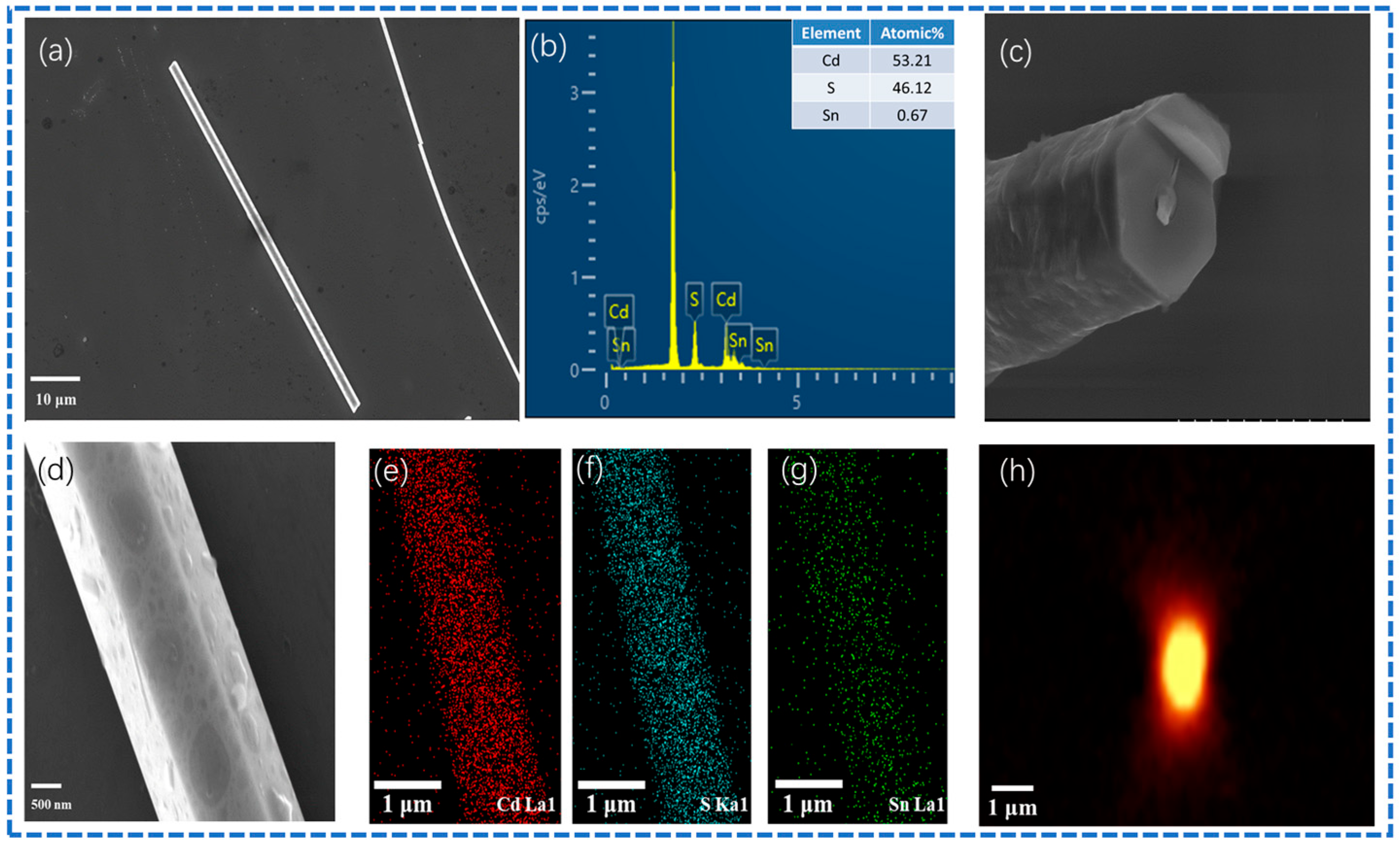
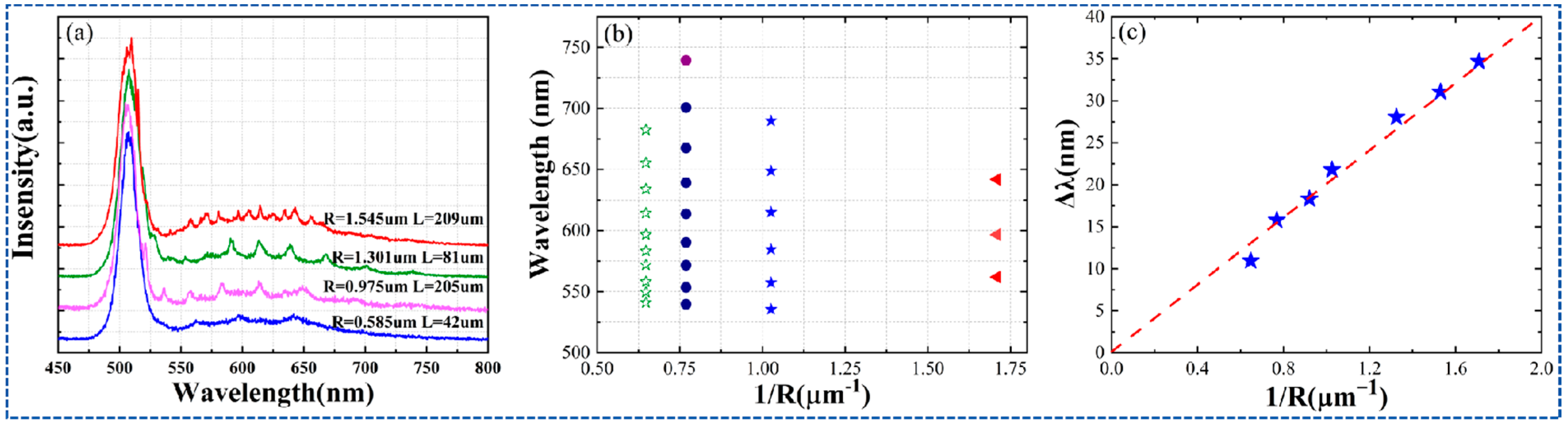
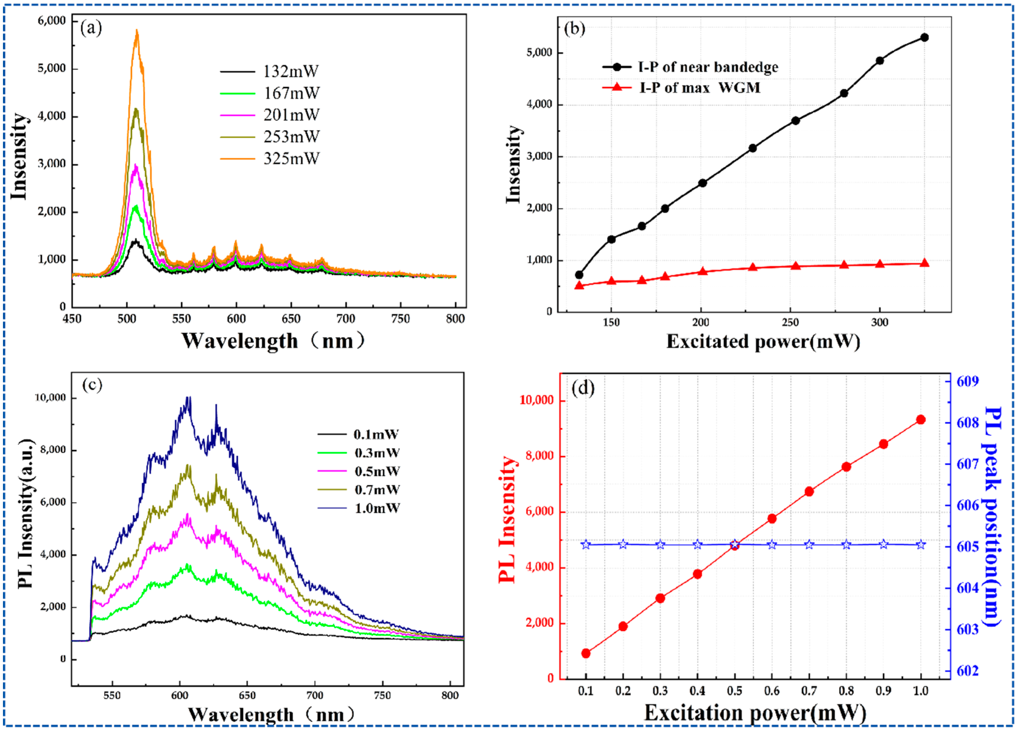
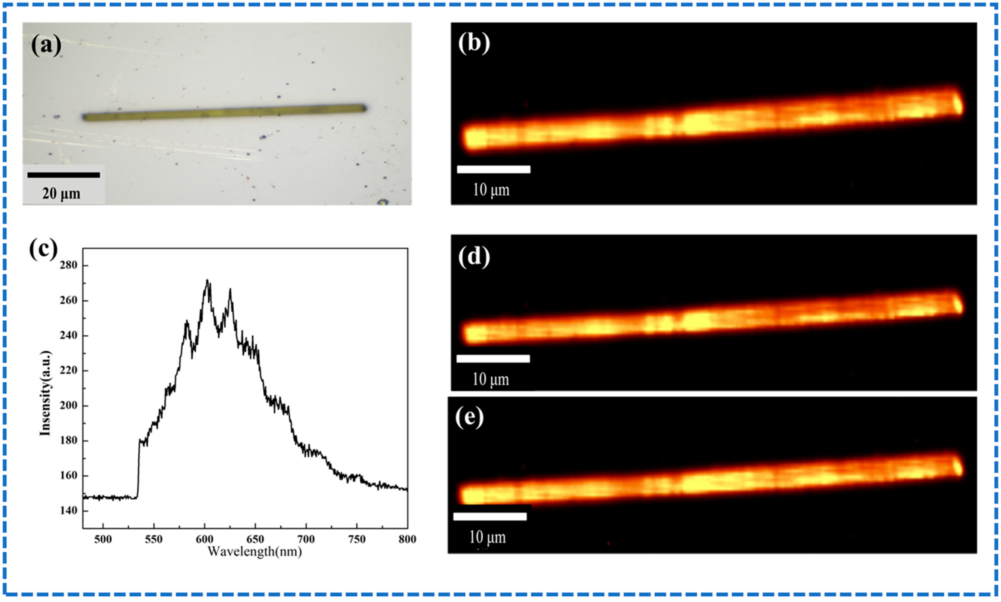
3. Results and Discussion

The scanning electron microscopy (SEM) image of the successfully synthesized CdS nanowires on a silicon substrate in this study is shown in Figure 1a. The synthesized nanowires display smooth and flat surfaces. Figure 1b presents the Energy-Dispersive X-ray Spectroscopy distribution profiles of each element contained in the synthesized CdS nanowire. As indicated in the figure, the element composition analysis of the CdS nanowire reveals that the contents of Cd, S, and Sn are 53.21%, 46.12%, and 0.67%, respectively. The results of EDS analysis confirmed that the nanowires are mainly composed of CdS, the ratio of Cd and S elements is close to the theoretical compound ratio, and the presence of trace Sn elements indicates that Sn has been effectively doped into the CdS nanowires. The cross-section SEM image of the synthesized Sn-doped CdS nanowires is shown in Figure 1c. As can be seen from the image, the cross-section of the nanowires presents a distinct hexagonal shape, and this continuous structure is very beneficial for the formation of WGM micro-cavities [28]. In order to further investigate the detailed distribution of elements within the nanowires, the SEM image along the length direction and the corresponding element mapping of Cd, S, and Sn of the synthesized CdS nanowires were measured, as shown in Figure 1d–g. Along the length direction of the nanowire, the Cd, S, and Sn elements are uniformly distributed, and the side of the nanowire presents a clearly hexagonal shape, which is exactly the same as the shape of a conventional CdS nanowire. This result indicates that we have successfully prepared Sn-doped CdS nanowires with micro-cavity structures. Moreover, no substrate coated with an Au thin film was employed for product collection. Based on the SEM and EDS findings, we postulate that Sn plays a pivotal role in nanowire growth. This resembles the comb-like growth of CdS observed when a mixture of SnO2 and CdS powder is used as the source material. Consequently, the current Sn-doped CdS nanowires adhere to the vapor–liquid–solid (VLS) growth mechanism [29,30,31]. Accordingly, Sn catalyst particles or droplets serve as efficient nucleation sites, driving the growth of CdS nanowires. Figure 1h presents the cross-sectional PL mapping of the CdS nanowire doped with Sn, corresponding to Figure 1c. This further provides a more intuitive confirmation that the cross-section is a regular hexagon.
The CdS nanowires doped with Sn of different sizes can be obtained by optimizing the content of Sn and the temperature parameters during the fabrication process of the nanowires. Figure 2a presents the photoluminescence spectra of four CdS nanowires doped with Sn of different sizes. We use the helium–cadmium laser to record photoluminescence spectra. The sizes of these four nanowires are radius 1.545 µm, length 209 µm, radius 1.301 µm, length 81 µm, radius 0.975 µm, length 205 µm, and radius 0.585 µm, length 42 µm. The lengths and diameters of the nanowires were measured using charge-coupled device (CCD) measurements conducted on each nanowire. From the PL spectrum, we can find that the spacing between the observed undulations is increasing with decreasing nanowire radius. And, it is not directly related to the change in the length of micrometer lines. The measurement result shows that a larger diameter of semiconductor nanowires results in reduced spacing between interference peaks, and at the same time, within the same spectral range, the number of resonance modes also increases accordingly. Moreover, as the length of the nanowire increases, the peak of the mode becomes sharper, indicating that a relatively large cavity size can improve the mode quality. Figure 2b illustrates the variation in peak positions as a function of the reciprocal radius of the nanowires, which is crucial for understanding the structural properties of the nanomaterials. While the mode spacing (Δ λ ) generally increases with decreasing cavity radius, this trend does not align with the photon mode of the sub-wavelength Fabry–Perot cavities, where Δ λ remains constant at each radius [32].
For all the investigated nanowires, the relationship between the mode spacing and the reciprocal of the synthesized CdS nanowires exhibits a linear pattern, as shown in Figure 2c. This is a characteristic feature of WGM-type cavity modes. For a typical hexagonal WGM micro-cavity, the Δλ, which represents the mode spacing, can be approximated using the method described in the reference, which utilizes the derivative of the size parameter to express the spacing between adjacent modes, and its expression can be represented as follows [33]:
λ = λ 2 3 3 n g L
where n g represents the group refractive index and λ represents the resonance wavelength. As shown in Figure 2c, by conducting a fitting analysis on the data, a result of approximately 3.4 for the group refractive index n g can be obtained. Moreover, the data analysis results show that a significant linear relationship between the mode spacing Δλ and the reciprocal of the nanowires’ radius can be found. Therefore, when the emission wavelength is fixed, the spacing Δλ has an inverse proportional relationship with the radius of the nanowires. This is mainly attributed to the fact that the radius of the micro-cavity is directly determined by the size of the nanowires. According to the above Formula (1), the inverse relationship between the mode spacing and the effective radius of the synthesized CdS nanowires is further confirmed. This indicates that within the same spectral range, the number of resonance modes will show a linearly increasing relationship with the side radius of the nanowires. The theoretical calculation results are consistent with the PL spectrum results. Together, these results and theoretical calculations demonstrate that the WGM micro-cavity can be formed along the radial axis of the CdS nanowires synthesized in this study, as evidenced by the resonance peak positions and mode patterns characteristic of WGM in cylindrical micro-cavities.
In order to carry out a comprehensive and in-depth investigation into the fundamental mechanism of forming micro-cavities of the synthesized CdS nanowires, the angle-resolved μ-PL of the CdS nanowires doped with Sn was measured at room temperature. Figure 3a presents the test schematic diagram of the angle-resolved μ-PL device constructed using Fourier optics technology. The formation of the Fourier plane (far-field) image is achieved through the use of two lenses and a microscope lens, by performing three Fourier transforms, and is ultimately projected onto the slit of the monochromator. Specifically, the coherent light emitted from the synthesized CdS nanowires is focused on the Fourier plane of a 100× magnification microscope objective lens with a numerical aperture of 0.8. The information related to the emission angles obtained via Fourier optical transformation is presented on this plane. Subsequently, the coherent light passes through two lenses and is projected onto the entrance slit of the monochromator [34]; thereby, a Fourier plane (far-field) image is formed on the slit. In the angle-resolved μ-PL device, we use the helium–cadmium laser to record photoluminescence spectra. Based on the varying relative orientations between the entrance slit of the monochromator and the radial direction of the synthesized CdS nanowires, two signal collection configurations have been developed, as shown in Figure 3b,c. In these two configurations, the longitudinal axis of the inlet slit remains unchanged and is marked as ‘a’-axis. The light-emitting side prism that functions as a reflective mirror for the planar micro-cavity mode is labeled as the ‘y’-axis [35]. For the configuration of y//a, the E(ϕ)–ϕ dispersion of the ARPL images obtained from the side-facets of the synthesized nanowires was recorded, as shown in Figure 3d–g. Among them, ϕ represents the photon collection angle in the y-z plane (Figure 3b). Meanwhile, under the y//a configuration, parabolic-like curves were observed on the low-energy side of the secondary electron peak. For the configuration of y⊥a (Figure 3c), the E(θ)–θ dispersion of the ARPL images is also recorded, as displayed in Figure 3h–k. The interference fringes were also observed on the low-energy side of the secondary electron peak; among them, ϕ represents the collection angle in the x-z plane [36]. According to the reported literature, for the configuration of y//a, the parabolic curves can be well fitted by the dispersion relation of the in-plane cavity photon. However, for the configuration of y⊥a, similar to the optimized Young’s double-slit experiment results, the generation of the interference fringes can be attributed to the phase difference existing between the wavelengths of the coherent emission light emitted from the two light-emitting sides [37,38].
Furthermore, the origin of the micro-cavity can also be distinguished by analyzing the changes in the excitation power and the photoluminescence spectrum. Figure 4a shows the relationship between the photoluminescence spectra of the synthesized CdS nanowires in this study and different excitation powers when excited by a helium–cadmium laser at room temperature (the radius R of the synthesized CdS nanowires is 1.301 μm, and the length L is 81 μm). The intensities of in-gap emission and band-edge emission peaks under varying excitation power, as depicted in Figure 4b, are derived from the data presented in Figure 4a. As shown in Figure 4b, with the increase in excitation power, the intensity increase rate of the band-edge emission is faster than that of the in-gap emission. The difference in the intensity growth trends of these two phenomena was also observed in the CdS nanobelts doped with Zn [39]. The variation relationship between the excitation power and the photoluminescence spectra of the synthesized CdS nanowires is shown in Figure 4c. Figure 4d illustrates the variation of the photoluminescence intensity of in-gap emission and the photoluminescence peak position shift of the excitation wavelength as the excitation power changes. As can be seen in Figure 4d, the intensity of in-gap emission photoluminescence increases linearly with the excitation power, while the excitation power has little effect on the position shift of the photoluminescence peak of the excitation wavelength; that is, as the excitation power increases, the peak position remains almost unchanged. This phenomenon precisely conforms to the characteristics of a classical micro-cavity, in which the contribution of the excitation power to the micro-cavity energy is very small [40].
Despite WGM cavity formation, lasing was not observed in the studied NWs under continuous wave excitation with power densities below 1.0 mW, in contrast to recent advancements where lasing has been achieved in similar nanostructures. The onset of lasing usually leads to a sudden narrowing of the PL line width. In fact, the main feature of the occurrences of the laser phenomenon is a sudden reduction in the width of the photoluminescence spectral line (or the appearance of a sharp peak on the background of spontaneous emission), as well as an ultra-linear increase in photoluminescence intensity with the increase in the excitation power [41,42,43,44]. On the contrary, in the synthesized CdS nanowires in this study, it can be observed that the emission intensity of the micro-cavity mode is almost linearly related to the increase in excitation power. In addition, in this study, no stimulated emission phenomenon was observed for the synthesized CdS nanowires. This might be attributed to a variety of factors, such as the material composition and the conditions under which these structures were exposed to light. Firstly, this might indicate that the oscillator intensity of the optical transition in the synthesized CdS nanowires in this study is relatively low. Although CdS is a direct band-gap material, its luminescence at room temperature is mainly attributed to the exciton recombination captured in various N-related centers. However, due to the limitation of N-related localized state density, the distribution of its localized state density is rather extensive. This luminescence efficiency is not as outstanding as the inter-band radiative recombination commonly found in the direct band-gap semiconductors (such as GaAs, InP, and GaN). Secondly, during the process of luminescence, longitudinal light propagation dominates rather than the oscillation of localized plasma modes. Therefore, all these factors need to be further finely adjusted and optimized, such as including the exploration of the relevant process parameters during the growth process, in order to achieve the generation of laser effects from the synthesized CdS nanowires.
The PL mapping technique allows for gaining insights into the composition of a nanowire at the micro-scale, particularly illustrating the dopant distribution both along and across doped nanowires [45]. In this study, the CdS nanowires doped with Sn, with a length of 81 μm and a radius of 1.301 μm, were successfully synthesized. The bright-field optical image of the synthesized CdS nanowires is shown in Figure 5a. Figure 5b presents the PL mapping spectrum excited by the helium–cadmium laser with the wavelength range from 533 to 800 nm. Figure 5c shows the corresponding micro-PL spectrum, which demonstrates the character of WGM. Figure 5d,e illustrate the mapping images of the peak region (593–601 nm) and valley region (602–613 nm), respectively, revealing the uneven distribution of bright and dark areas due to the unique field distribution of whispering-gallery mode (WGM) on the microrod surface. One typical feature of the WGM micro-cavity observed in wire-shaped nanostructured semiconductor materials is that light can freely propagate along the axial region, but its propagation in the radial direction will be restricted. Further detailed observation reveals that periodic sawtooth patterns are observed on the surface of the PL mapping diagram, and each pair of sawteeth forms a two-dimensional (2D) plate-like cavity. Therefore, this three-dimensional cylindrical waveguide mode can be regarded as an array composed of countless two-dimensional cylindrical waveguides arranged along their axial direction, and each plate cavity forms a WGM micro-cavity. Due to the small mode volume and high-Q factor, we estimate that the quality factor of the WGM peak is approximately 70. Last, but equally important, in the axial direction of the synthesized CdS nanowires, there may exist multiple Fabry–Perot (F-P) micro-cavities. The potential Fabry–Perot (FP) cavities along the nanowire axis were proved by PL mapping. We can see strong PL intensity at both ends of the micrometer line in PL mapping, which may be due to the F-P micro-cavity [17]. However, since our test is an in situ test, it is difficult to distinguish it from a spectral perspective. Similar lines have also been observed in other experiments. From the PL mapping image of the synthesized CdS nanowires, we found that in some parts of the synthesized CdS nanowires, luminescence was enhanced and showed an irregular distribution, which may be due to the non-uniformity of Sn doping. All of these factors could lead to the selective strengthening of certain modes and cause the emission intensity of specific modes (such as WGM and F-P) to continuously increase [46]. In our nanowires, the WGM mode micro-cavities are dominant. Compared to the F-P mode micro-cavities, the WGM mode micro-cavities exhibit radial total internal reflection (TIR) along the hexagonal perimeter. This will generate high-Q resonance with light confined near the surface of the nanowires. FP mode micro-cavities rely on axial end face reflection and are radius-independent. The WGM mode micro-cavity feedback originates from continuous TIR along curved boundaries, achieving low-loss cycling. FP mode micro-cavities rely on discrete specular reflection for feedback, and due to diffraction, they suffer higher losses at sub-wavelength scales.

4. Conclusions

In summary, we have devised a straightforward method to synthesize CdS nanowires featuring a regular hexagonal cross-section. Through the application of µ-PL measurements on individual nanowires and SEM analysis, our research has demonstrated that Sn-doped CdS nanowires can serve as WGM micro-cavities, a finding that aligns with the tunable performance of WGM micro-cavities as discussed in optical studies. Cross-section PL mapping of the Sn-doped CdS nanowire further demonstrated that the synthesized CdS nanowires maintain a hexagonal cross-section, as similarly observed in undoped CdS nanowires. When the laser excitation wavelength is fixed, the reciprocal of the nanowire radius is in a proportional relationship with the mode spacing. The number of resonant modes increases as the radius of CdS nanowires increases. This leads to a significant improvement in ARPL imaging, leveraging Fourier optics principles. When using the two collection configurations of ARPL, the WGM mode micro-cavity becomes discernible at higher collection angles as the excitation power increases. The excitation power-dependent wavelength shift, intensity shift, and PL mapping further demonstrated that the as-prepared Sn-doped CdS nanowires can form a high-quality WGM micro-cavity. Despite the inability to detect stimulated emissions, our findings have paved the way for alternative methods to characterize semiconductor micro-cavity modes. Furthermore, the observation of WGM micro-cavity modes in the synthesized CdS nanowires marks a significant step towards the realization of lasing and photonic chip devices incorporating semiconductor resonators.

Author Contributions

Validation, T.L. (Ting Liang); Formal analysis, Z.L. and Y.T.; Investigation, Z.L., Y.T., F.L. and T.L. (Tengteng Li); Data curation, C.L.; Writing—original draft, J.Y. and T.L. (Tengteng Li); Writing—review & editing, C.L. and T.L. (Ting Liang); Project administration, J.Y. All authors have read and agreed to the published version of the manuscript.

Funding

This research was supported by the Key Research and Development Program of Shanxi Province (Grant No. 202302030201001) and the science and technology major Program of Shanxi Province (Grant No. 202301030201003).

Data Availability Statement

No new data were created or analyzed in this study.

Acknowledgments

Thanks to the above funds.

Conflicts of Interest

The authors declare no conflicts of interest.

References

  1. Qian, F.; Li, Y.; Gradečak, S.; Park, H.G.; Dong, Y.; Ding, Y.; Wang, Z.L.; Lieber, C.M. Multi-quantum-well nanowire heterostructures for wavelength-controlled lasers. Nat. Mater. 2008, 7, 701–706. [Google Scholar] [CrossRef] [PubMed]
  2. No, Y.-S. Electrically Driven Micro- and Nano-Scale Semiconductor Light Sources. Appl. Sci. 2019, 9, 802. [Google Scholar] [CrossRef]
  3. Baimukhanov, Z.; Dauletbekova, A.; Junisbekova, D. Synthesis of Orthorhombic Tin Dioxide Nanowires in Track Templates. Materials 2024, 17, 1226. [Google Scholar] [CrossRef] [PubMed]
  4. Cao, B.; Tian, Y.; Wen, H.F.; Guo, H.; Wu, X.Y.; Li, L.; Zhang, Z.; Liu, L.; Zhu, Q.; Tang, J. Recent progress on fabrication, spectroscopy properties, and device applications in Sn-doped CdS micro-nano structures. J. Semicond. 2024, 45, 091101. [Google Scholar] [CrossRef]
  5. Yan, H.; Choe, H.S.; Nam, S.W.; Hu, Y.; Das, S.; Klemic, J.F.; Ellenboge, J.C.; Lieber, C.M. Programmable nanowire circuits for nanoprocessors. Nature 2011, 470, 240–244. [Google Scholar] [CrossRef] [PubMed]
  6. Liu, X.; Xu, P.; Wu, Y.; Yang, Z.; Meng, C.; Yang, W.; Li, J.; Wang, D.; Liu, X.; Yang, Q. Control, optimization and measurement of parameters of semiconductor nanowires lasers. Nano Energy 2015, 14, 340–354. [Google Scholar] [CrossRef]
  7. Friedman, R.S.; McAlpine, M.C.; Ricketts, D.S.; Ham, D.; Lieber, C.M. High-speed integrated nanowire circuits. Nature 2005, 434, 1085. [Google Scholar] [CrossRef] [PubMed]
  8. Sirbuly, D.J.; Law, M.; Pauzauskie, P.; Yan, H.; Maslov, A.V.; Knutsen, K.; Ning, C.Z.; Saykally, R.J.; Yang, P. Optical routing and sensing with nanowire assemblies. Proc. Natl. Acad. Sci. USA 2005, 102, 7800–7805. [Google Scholar] [CrossRef] [PubMed]
  9. Pan, A.; Zhou, W.; Leong, E.S.P.; Liu, R.; Chin, A.H.; Zou, B.; Ning, C.Z. Continuous alloy-composition spatial grading and superbroad wavelength-tunable nanowire lasers on a single chip. Nano Lett. 2009, 9, 784–788. [Google Scholar] [CrossRef] [PubMed]
  10. Zhang, M.; Wille, M.; Röder, R.; Heedt, S.; Jia, G.L. Amphoteric nature of Sn in CdS nanowires. Nano Lett. 2014, 14, 518–523. [Google Scholar] [CrossRef] [PubMed]
  11. Agarwal, R.; Barrelet, C.J.; Lieber, C.M. Lasing in single cadmium sulfide nanowire optical cavities. Nano Lett. 2005, 5, 917–920. [Google Scholar] [CrossRef] [PubMed]
  12. Liu, X.; Zhang, Q.; Xiong, Q.; Sum, T.C. Tailoring the lasing modes in semiconductor nanowire cavities using intrinsic self-absorption. Nano Lett. 2013, 13, 1080–1085. [Google Scholar] [CrossRef] [PubMed]
  13. Tian, Y.; Yao, S.; Zou, B. Excitation-Power-Dependent Color Tuning in a Single Sn-Doped CdS Nanowire. Molecules 2024, 29, 5389. [Google Scholar] [CrossRef] [PubMed]
  14. Tian, Y.; Yao, S.; Zhou, Z.; Peng, H.; Ke, B.; Zhou, W.; Zhang, Y.; Zou, B. Super-Broad-Wavelength-Range Polarization-Selective Exciton-Polariton in Sn-Doped CdS Nanowires. ACS Appl. Opt. Mater. 2023, 1, 298–305. [Google Scholar] [CrossRef]
  15. Zhang, L.; Zhang, Y.; Guo, Y.; Wang, Y.; Liu, R.; Chen, B.; Zhong, H.; Zou, B. Growth of CdS nanotubes and their strong optical microcavity effects. Nanoscale 2019, 11, 5325–5329. [Google Scholar] [CrossRef] [PubMed]
  16. Zhang, Q.; Wang, S.W.; Liu, X.; Chen, T.; Li, H.; Liang, J.; Zheng, W.; Agarwal, R.; Lu, W.; Pan, A. Low threshold, single-mode laser based on individual CdS nanoribbons in dielectric DBR microcavity. Nano Energy 2016, 30, 481–487. [Google Scholar] [CrossRef]
  17. Xu, T.; Lv, Q.; Li, X.; Xu, Z.; Xin, W.; Shen, X.; Guo, P.; Xiao, L. Formation of CdS/Sn Superlattice Nanowires and Room-Temperature Microcavity Stimulated Emission. ACS Appl. Nano Mater. 2025, 8, 7235–7242. [Google Scholar] [CrossRef]
  18. Feng, C.; Xu, Z.; Wang, X.; Yang, H.; Fu, H. Organic-nanowire–SiO2 core–shell microlasers with highly polarized and narrow emissions for biological imaging. Acs Appl. Mater. Interfaces 2017, 9, 7385–7391. [Google Scholar] [CrossRef] [PubMed]
  19. Che, K.-J.; Huang, Y.-Z. Mode characteristics of metallically coated square microcavity connected with an output waveguide. J. Appl. Phys. 2010, 107, 113103. [Google Scholar] [CrossRef]
  20. Baek, H.; Hyun, J.K.; Chung, K.; Oh, H.; Yi, G.C. Selective excitation of Fabry-Perot or whispering-gallery mode-type lasing in GaN microrods. Appl. Phys. Lett. 2014, 105, 201108. [Google Scholar] [CrossRef]
  21. Dai, G.; Zhang, Y.; Liu, R.; Qiang, W.; Zhang, Q.; Pan, A.; Zou, B. Visible whispering-gallery modes in ZnO microwires with varied cross sections. J. Appl. Phys. 2011, 110, 033101. [Google Scholar] [CrossRef]
  22. Liu, Y.; Dong, H.; Sun, S.; Liu, W.; Zhan, J.; Chen, Z.; Wang, J.; Zhang, L. Optical modulation of ZnO microwire optical resonators with a parallelogram cross-section. Nanoscale 2013, 5, 4123–4128. [Google Scholar] [CrossRef] [PubMed]
  23. Shang, Q.; Zhang, S.; Liu, Z.; Chen, J.; Yang, P.; Li, C.; Li, W.; Zhang, Y.; Xiong, Q.; Liu, X.; et al. Surface plasmon enhanced strong exciton–photon coupling in hybrid inorganic–organic perovskite nanowires. Nano Lett. 2018, 18, 3335–3343. [Google Scholar] [CrossRef] [PubMed]
  24. Takazawa, K.; Inoue, J.; Mitsuishi, K.; Takamasu, T. Fraction of a millimeter propagation of exciton polaritons in photoexcited nanofibers of organic dye. Phys. Rev. Lett. 2010, 105, 067401. [Google Scholar] [CrossRef] [PubMed]
  25. Zhang, Y.; Zhou, H.; Liu, S.W.; Tian, Z.R.; Xiao, M. Second-harmonic whispering-gallery modes in ZnO nanotetrapod. Nano Lett. 2009, 9, 2109–2112. [Google Scholar] [CrossRef] [PubMed]
  26. Tessarek, C.; Röder, R.; Michalsky, T.; Geburt, S.; Franke, H.; Schmidt-Grund, R.; Heilmann, M.; Hoffmann, B.; Ronning, C.; Grundmann, M.; et al. Improving the optical properties of self-catalyzed GaN microrods toward whispering gallery mode lasing. ACS Photonics 2014, 1, 990–997. [Google Scholar] [CrossRef]
  27. Czekalla, C.; Sturm, C.; Schmidt-Grund, R.; Cao, B.Q.; Lorenz, W.; Grundmann, M. Whispering gallery mode lasing in zinc oxide microwires. Appl. Phys. Lett. 2008, 92, 241102. [Google Scholar] [CrossRef]
  28. Nobis, T.; Kaidashev, E.M.; Rahm, A.; Lorenz, M.; Grundmann, M. Whispering gallery modes in nanosized dielectric resonators with hexagonal cross section. Phys. Rev. Lett. 2004, 93, 103903. [Google Scholar] [CrossRef] [PubMed]
  29. Liu, R.; Li, Z.A.; Zhang, C.; Wang, C.; Kamran, M.A.; Farle, M.; Zou, B. Single-step synthesis of monolithic comb-like CdS nanostructures with tunable waveguide properties. Nano Lett. 2013, 13, 2997–3001. [Google Scholar] [CrossRef] [PubMed]
  30. Wu, Y.; Yang, P. Direct observation of vapor−liquid−solid nanowire growth. J. Am. Chem. Soc. 2001, 123, 3165–3166. [Google Scholar] [CrossRef]
  31. Wagner, R.S.; Ellis, W.C. Vapor-Liquid-Solid mechanism of single crystal growth (New method growth catalysis from impurity whiker epitaxial large cystals). Appl. Phys. Lett. 1964, 4, 89–90. [Google Scholar] [CrossRef]
  32. Evans, T.J.S.; Schlaus, A.; Fu, Y.; Zhou, X.; Atallah, T.L.; Spencer, M.S.; Brus, L.E.; Jin, S.; Zhu, X.Y. Continuous-wave lasing in cesium lead bromide perovskite nanowires. Adv. Opt. Mater. 2018, 6, 1700982. [Google Scholar] [CrossRef]
  33. Bhowmik, A.K. Polygonal optical cavities. Appl. Opt. 2000, 39, 3071–3075. [Google Scholar] [CrossRef] [PubMed]
  34. Gong, S.H.; Ko, S.M.; Jang, M.H.; Cho, Y.H. Giant rabi splitting of whispering gallery polaritons in GaN/InGaN core–shell wire. Nano Lett. 2015, 15, 4517–4524. [Google Scholar] [CrossRef] [PubMed]
  35. Sun, L.; Sun, S.; Dong, H.; Xie, W.; Richard, M.; Zhou, L.; Dang, L.S.; Shen, X.; Chen, Z. Room temperature one-dimensional polariton condensate in a ZnO microwire. Br. J. Radiol. 2010, 67, 605–608. [Google Scholar]
  36. Li, Q.; Li, C.; Shang, Q.; Zhao, L.; Zhang, S.; Gao, Y.; Liu, X.; Wang, X.N.; Zhang, Q. Lasing from reduced dimensional perovskite microplatelets: Fabry-Pérot or whispering-gallery-mode? J. Chem. Phys. 2019, 151, 211101. [Google Scholar] [CrossRef] [PubMed]
  37. Sun, L.; Ren, M.; Liu, W.; Agarwal, R. Resolving parity and order of fabry–pérot modes in semiconductor nanostructure waveguides and lasers: Young’s interference experiment revisited. Nano Lett. 2014, 14, 6564–6571. [Google Scholar] [CrossRef] [PubMed]
  38. Xu, D.; Liu, W.; Zhang, S.; Shen, X.; Chen, Z. Three-dimensional confinement of polaritons in ZnO microcylinder. Opt. Express 2013, 21, 3911–3916. [Google Scholar] [CrossRef] [PubMed]
  39. Wang, X.; Zhang, W.; Song, G.; Zou, B.; Li, Z.; Guo, S.; Li, J.; Li, Q.; Liu, R. Visual monitoring of laser power and spot profile in micron region by a single chip of Zn-doped CdS nanobelts. RSC Adv. 2014, 4, 52550–52554. [Google Scholar] [CrossRef]
  40. Zheng, Q.; Zhou, W.; Peng, Y.; Yin, Y.; Zhong, M.; Zhao, Z.; Zhang, Q.; Tang, D.; Zeng, R.; Zou, B. Surface polarons and optical micro-cavity modulated broad range multi-mode emission of Te-doped CdS nanowires. Nanotechnology 2018, 29, 465709. [Google Scholar] [CrossRef] [PubMed]
  41. Saxena, D.; Mokkapati, S.; Parkinson, P.; Jiang, N.; Gao, Q.; Tan, H.H.; Jagadish, C. Optically pumped room-temperature GaAs nanowire lasers. Nat. Photonics 2013, 7, 963–968. [Google Scholar] [CrossRef]
  42. Duan, X.; Yu, H.; Agarwal, R.; Lieber, C.M. Single-nanowire electrically driven lasers. Nature 2003, 421, 241–245. [Google Scholar] [CrossRef] [PubMed]
  43. Zhang, L.; Liu, R.; Zou, B. Sn-Doped CdS Nanowires with Low-Temperature Lasing by CW-Laser Excitation. ACS Appl. Electron. Mater. 2019, 2, 282–289. [Google Scholar] [CrossRef]
  44. Geburt, S.; Thielmann, A.; Röder, R.; Borschel, C.; McDonnell, A.; Kozlik, M.; Kühnel, J.; Sunter, K.A.; Capasso, F.; Ronning, C. Low threshold room-temperature lasing of CdS nanowires. Nanotechnology 2012, 23, 365204. [Google Scholar] [CrossRef] [PubMed]
  45. Li, Y.; Dai, G.; Zhou, C.; Zhang, Q.; Wan, Q.; Fu, L.; Zhang, J.; Liu, R.; Cao, C.; Pan, A.; et al. Formation and optical properties of ZnO: ZnFe2O4 superlattice microwires. Nano Res. 2010, 3, 326–338. [Google Scholar] [CrossRef]
  46. Dai, G.; Zou, B.; Wang, Z. Preparation and periodic emission of superlattice CdS/CdS: SnS2 microwires. J. Am. Chem. Soc. 2010, 132, 12174–12175. [Google Scholar] [CrossRef] [PubMed]
Figure 1. (a) SEM image of a synthesized CdS nanowire; (b) the EDS distribution profiles of each element contained in the synthesized CdS nanowire; (c) schematic illustration of the cross-section of the synthesized CdS nanowire; (dg) the SEM image and corresponding Cd, S, Sn element mapping; (h) schematic illustration of cross-section PL mapping of Sn-doped CdS nanowire.
Crystals 15 00658 g001
Figure 2. (a) The PL spectra of four synthesized CdS nanowires with different sizes; (b) the variation in peak positions as a function of the reciprocal radius of the nanowires (The green star, blue star, red triangle, blue dot, and purple dot represent the Gaussian fitted peak wavelengths for nanowires with radii of 1.545 µm, 1.301 µm, 0.975 µm, length 205 µm, and radius 0.585 µm, respectively); (c) the difference between peak positions and the reciprocal of the nanowire radius.
Crystals 15 00658 g002
Figure 3. (a) Schematic of an angle-resolved PL setup using Fourier optics; (b,c) the y-axis of Sn-doped CdS nanowires is parallel (b) or perpendicular (c) to the a-axis of the entrance slit of the monochromator; (dg) the ARPL images with P of (d) 134 mW, (e) 168 mW, (f) 241 mW, (g) 326 mW for the configuration of y//a; (hk) the ARPL images with P = (h) 134 mW, (i) 168 mW, (j) 241 mW, (k) 326 mW for the configuration of y⊥a.
Crystals 15 00658 g003
Figure 4. (a) The relationship between the PL spectrum of the Sn-doped CdS nanowire and the excitation power; (b) the intensities of in-gap emission and band-edge emission peaks under varying excitation power; (c) the power-dependent PL spectrum of the Sn-doped CdS nanowire excited by the helium–cadmium laser; (d) the intensity (I) of the max WGM peak and the peak position of max WGM versus excited power.
Crystals 15 00658 g004
Figure 5. (a) The CCD images of synthesized CdS nanowires (R = 1.301 μm, L = 81 μm); (b) the PL mapping spectrum excited by a helium–cadmium laser with the wavelength range from 533 to 800 nm; (c) the PL spectrum of synthesized CdS nanowires; (d) the PL mapping spectrum in the regions of 593–601 nm; (e) the PL mapping spectrum in the regions of 602–613 nm.
Crystals 15 00658 g005
Disclaimer/Publisher’s Note: The statements, opinions and data contained in all publications are solely those of the individual author(s) and contributor(s) and not of MDPI and/or the editor(s). MDPI and/or the editor(s) disclaim responsibility for any injury to people or property resulting from any ideas, methods, instructions or products referred to in the content.

