Article

Transport Properties of One-Dimensional van der Waals Heterostructures Based on Molybdenum Dichalcogenides

by
Daulet Sergeyev
1,2,* and
Kuanyshbek Shunkeyev
1
1
Department of Physics, K.Zhubanov Aktobe Regional University, Aktobe 030000, Kazakhstan
2
Department of General Engineering Disciplines, T.Begeldinov Aktobe Aviation Institute, Aktobe 030012, Kazakhstan
*
Author to whom correspondence should be addressed.
Crystals 2025, 15(7), 656; https://doi.org/10.3390/cryst15070656
Submission received: 27 May 2025 / Revised: 2 July 2025 / Accepted: 11 July 2025 / Published: 18 July 2025

Abstract

The transport properties of one-dimensional van der Waals nanodevices composed of carbon nanotubes (CNTs), hexagonal boron nitride (hBN) nanotubes, and molybdenum dichalcogenide (MoX2) nanotubes were investigated within the framework of density functional theory (DFT). It was found that in nanodevices based on MoS2(24,24) and MoTe2(24,24), the effect of resonant tunneling is suppressed due to electron–phonon scattering. This suppression arises from the fact that these materials are semiconductors with an indirect band gap, where phonon participation is required to conserve momentum during transitions between the valence and conduction bands. In contrast, nanodevices incorporating MoSe2(24,24), which possesses a direct band gap, exhibit resonant tunneling, as quasiparticles can tunnel between the valence and conduction bands without a change in momentum. It was demonstrated that the presence of vacancy defects in the CNT segment significantly degrades quasiparticle transport compared to Stone–Wales (SW) defects. Furthermore, it was revealed that resonant interactions between SW defects in MoTe2(24,24)–hBN(27,27)–CNT(24,24) nanodevices can enhance the differential conductance under certain voltages. These findings may be beneficial for the design and development of nanoscale diodes, back nanodiodes, and tunneling nanodiodes.

1. Introduction

The discovery of graphene has stimulated the search for new two-dimensional (2D) atomically thin crystals [1,2,3,4]. At present, the library of atomically thin materials is rapidly expanding with the addition of new two-dimensional and quasi-two-dimensional compounds exhibiting unusual electronic, optical, and mechanical properties [5,6,7]. This diversity of 2D materials has enabled the construction of a vast number of van der Waals (vdW) heterostructures, first proposed by Geim in 2013 [8,9,10]. By carefully selecting a specific sequence of atomic layers in advance, it has become possible to synthesize novel vdW nanomaterials with tailored electronic and optical properties [11,12,13]. It is worth noting that first-principles calculations have recently been widely applied to address such tasks [14,15,16,17], including their integration with machine learning (AI) methods, which allow for the reliable determination of quantum transport properties in such nanostructures [18,19].
While vdW heterostructures were previously realized only on the basis of (quasi-)2D materials, recent experiments have demonstrated the successful synthesis of 1D vdW heterostructures. For example, in [20], one-dimensional heterostructures were synthesized via chemical vapor deposition (CVD), where crystallized nanotubes based on hexagonal boron nitride (hBN) and molybdenum disulfide (MoS2) were grown on a single-walled carbon nanotube (SWCNT) template. In most cases, 1D structures in the form of nanotubes are obtained by rolling up their two-dimensional analogs [21]. However, the process of forming 1D structures through the rolling of 2D counterparts remains insufficiently studied. The successful implementation of this approach undoubtedly expands the range of available one-dimensional materials and the variety of 1D vdW heterodevices based on them. It should be noted that, compared to their 2D analogs, 1D vdW heterostructures are significantly limited by their radial dimensions. Moreover, the atoms in such structures experience internal strain due to their cylindrical geometry. These spatial constraints may give rise to new physical phenomena and potential applications, as they enhance quantum effects in 1D heterostructures, such as the giant bulk photovoltaic effect, increased flexoelectricity, and others [22,23].
At present, hBN nanotubes are widely used as dielectric components in the construction of vdW heterostructures [24]. Despite the existence of numerous potential dielectric nanomaterials—such as native oxides (WO3, MoO) [25] and ionic crystals (NaF, CaF2, MgF2, CdF2) [26,27,28,29,30]—hBN offers several key advantages. It possesses a hexagonal lattice with an atomic-scale thickness, and its lattice constant is nearly identical to that of graphene (only ~1.8% larger). In addition, it has a wide band gap of approximately 5.9eV. Beyond these properties, hBN is thermally and mechanically stable and exhibits high thermal conductivity [31]. These features undoubtedly make hBN a promising material for use as a gate dielectric or tunneling barrier in the development of novel nanoelectronic devices based on vdW heterostructures, as well as its application in optoelectronics and photonics, thermal management, batteries and supercapacitors, and other next-generation energy-efficient devices [32]. However, for the optimal operation of such nanoelectronic devices, the insulating layer must meet specific criteria: a low gate leakage current (<10−2 A/cm2), low interface trap density (<1010 cm−2 eV−1), low border trap density in the gate insulator (<1017 cm−3 eV−1), and high dielectric breakdown strength (>10 MV/cm) [24,27,33,34,35]. Based on its 2D analog, hBN nanotubes with diameters in the range of ~1–3 nm have been synthesized [36], and they have become essential components in 1D vdW heterodevices.
One of the most relevant classes of nanomaterials with semiconducting properties is the group of transition metal dichalcogenides (TMDs) with the general formula MeX2, where Me = Mo, W, Nb, etc., and X is a chalcogen (S, Se, Te) [37,38,39,40]. At low temperatures, below the critical temperature, some TMDs (e.g., NbS2, NbSe2, TaS2, TaSe2, and others) exhibit superconducting behavior [41,42]. This low-temperature behavior is of particular interest for studying superconductivity in low-dimensional (1D, 2D) systems, where unique effects associated with the superconducting state can emerge [43,44,45]. In contrast to other well-known 2D materials, such as graphene and hBN, monolayers of TMDs are three atoms thick, with a transition metal atom sandwiched between two chalcogen atoms. This structural feature makes it more challenging to roll them into nanotubes. It should also be noted that, in various quasi-1D vdW device architectures, monolayer materials such as transition metal monochalcogenides and trichalcogenides (TMMs) are used alongside TMDs [46,47]. When atomic sheets of transition metal monochalcogenidesare rolled into nanotubes, the strain energy induced by the curvature can be lower than that of TMDs or TMMs due to their smaller thickness. However, these materials typically have less symmetric structures [48].
TMD-based nanotubes exhibit a wide variety of electronic properties, functioning as metals, semimetals, semiconductors with different band gaps, or dielectrics [6,49]. By selecting appropriate sequences and combinations of TMD–1D structures, it becomes possible to modulate the properties of vdW devices and design ultraminiature heterojunctions, such as semiconductor–metal contacts, electron–hole junctions, and nanoscale sensors with dimensions of just a few nanometers. The properties of such materials can also be tuned by altering the misorientation angle between constituent atomic planes, leading to the emergence of moiré effects [50,51,52]. Despite the challenges in fabricating 1D TMD-based heterostructures, recent advances have led to the increased use of combined graphene, hBN, and TMD components in the design of low-dimensional vdW devices [53,54].
In [55], the role of monolayer hBN was experimentally demonstrated in scaled 2D transistors, showing that hBN can act as a passivation layer to suppress trap states originating from the environment. This enables nearly ideal subthreshold swing values (~62 mV/dec) and a narrow distribution with a standard deviation of 4.4 mV/dec in short-channel monolayer MoS2 transistors. In [56], a nonvolatile optoelectronic memory device was fabricated using WSe2 and Gr-based vdW heterostructures encapsulated in hBN. UV light and electric fields can easily modulate the operation of such a device. Soft actuators based on heterojunctions composed of WSe2 and grapheme nanosheets have been developed, exhibiting various modes of motion driven by near-infrared laser irradiation [57]. These distinct modes of actuation are enabled by the deformation induced via the photothermal effect, allowing the system to adapt to different operating conditions. Furthermore, ref. [58] reports the study of resonant energy transfer processes between vdW nanostructures from two fundamentally different systems: single-photon emitters in 2D hBN and excitons in TMD monolayers. It was shown that color centers in hBN interact with TMD excitons, enabling their application in the development of next-generation nanophotonic devices.
It is worth noting that TMDs can alter their transport properties when interacting with certain 2D materials. For example, the combination of molybdenum disulfide and silicene results in an unusual nanosystem exhibiting predominantly metallic behavior [59,60].
The transport properties of 1D heterodevices can be significantly affected by structural imperfections (defects) in the channel, interface, or other components. For instance, multiple localized defect states with varying energy levels within the band gap can create tunneling paths across the hBN barrier. Such interface traps located in the hBN layer may lead to leakage currents, threshold voltage instabilities, 1/f-noise [61], hysteresis [62], long-term drift [63], and other reliability issues. Structural imperfections in CNTs also play an important role in charge transport [64]. In our previous studies, we investigated the influence of various types of defects—such as Stone–Wales (SW) defects, vacancies, and others—on the current–voltage and other transport characteristics of CNTs [65,66]. It was shown that scattering on these defects degrades mobility, and in [25] it was established that the fast charge exchange between defect sites and the channel contributes to subthresholdfluctuations. In the present work, we investigate from first principles the influence of structural imperfections in CNTs on the transport properties of 1D vdW heterostructures based on MoX2–hBN–CNT.

2. Methods

The band structure of the nanotubes was calculated within the framework of DFT-GGA using the Perdew–Burke–Ernzerhof (PBE) exchange–correlation functional along the high-symmetry path Γ–Z in the Brillouin zone, employing the AtomistixToolKit with Virtual NanoLab 2015.1 software package.
Computer modeling of the transport characteristics of 1D heterostructures was performed within the framework of density functional theory (DFT) combined with the non-equilibrium Green’s function (NEGF) formalism and employing the local density approximation (LDA) [67,68]. To calculate the current–voltage characteristics (CVCs) and differential conductance, the transmission spectrum T ε of the nanodevice under consideration was first determined as
T ε = t r Γ L G Γ R G = t r Γ R G Γ L G ,
where Γ L R ε is the broadening matrices (broadening functions) of the left (right) electrodes, and G ε and G ε are the retarded and advanced Green’s functions. The CVC of the nanostructure was then computed using the well-known Landauer formula, which describes the fundamental relationship between electrical current and the transmission spectrum:
I V L ,   V R ,   T L ,   T R = 2 e h + T E f E μ R k B T R f E μ L k B T L d E ,
where k B is the Boltzmann constant, T L and T R are the Fermi–Dirac distribution functions, and μ R and μ L are the electrochemical potentials of the left and right electrodes, respectively.
The differential conductance of the nanostructure was obtained by computing the self-consistent current under a series of applied bias voltages followed by numerical differentiation:
σ V b i a s ,   T L ,   T R = I V b i a s 1 ,   T L ,   T R I V b i a s 2 ,   T L ,   T R V b i a s 1 V b i a s 2 .
To determine the density of states (DOS) of the nanotubes, the local density of states (LDOS) is first calculated as
D ε , r = i j ρ i j ε ϕ i r ϕ j r .
where ρ ε = ρ L ε + ρ R ε and ϕ r are the basis orbitals. The DOS of the nanotubes is then obtained by integrating the LDOS over the entire space:
D ε = d r D ε = i j ρ i j ε S i j
where S i j = ϕ i r ϕ j r d r is the overlap matrix.
The electronic transport calculations were performed using a Poisson solver and Brillouin zone integration with a k-point sampling grid of (1, 1, 100). A cutoff energy of 75 Hartree was used for the real-space grid, and the convergence criteria for forces and energy were set to 10−6.
All simulations were carried out on a Supermicro server (Super Micro Computer, Inc., San Jose, CA, USA, distributor PolyWorks Company) equipped with an Intel® Xeon® Silver processor, 512 GB of RAM, and 64 cores. Modeling of the transport characteristics of the nanoheterostructures was implemented using the Atomistix ToolKit with Virtual NanoLab software [69]. The fundamental equations of this method are described in detail in [70,71,72].

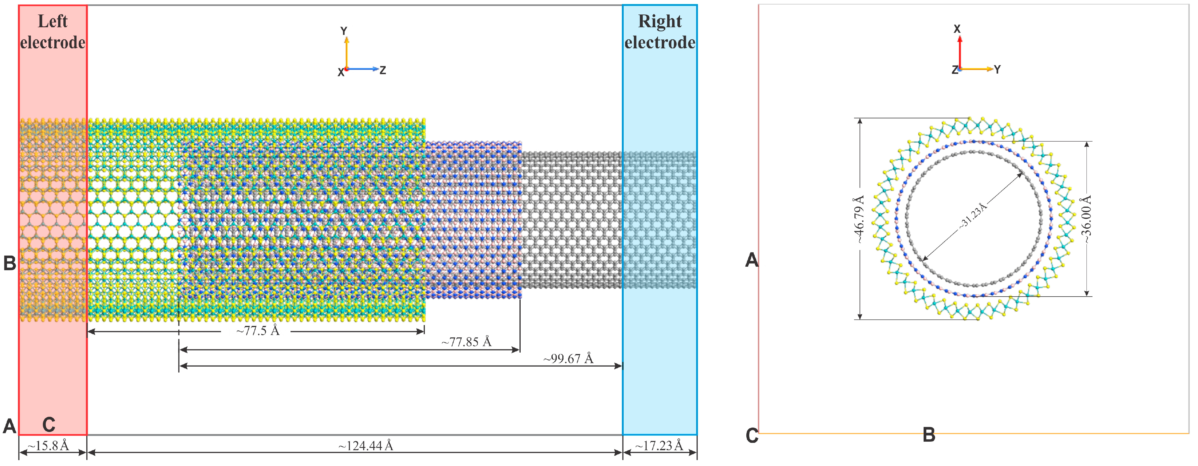
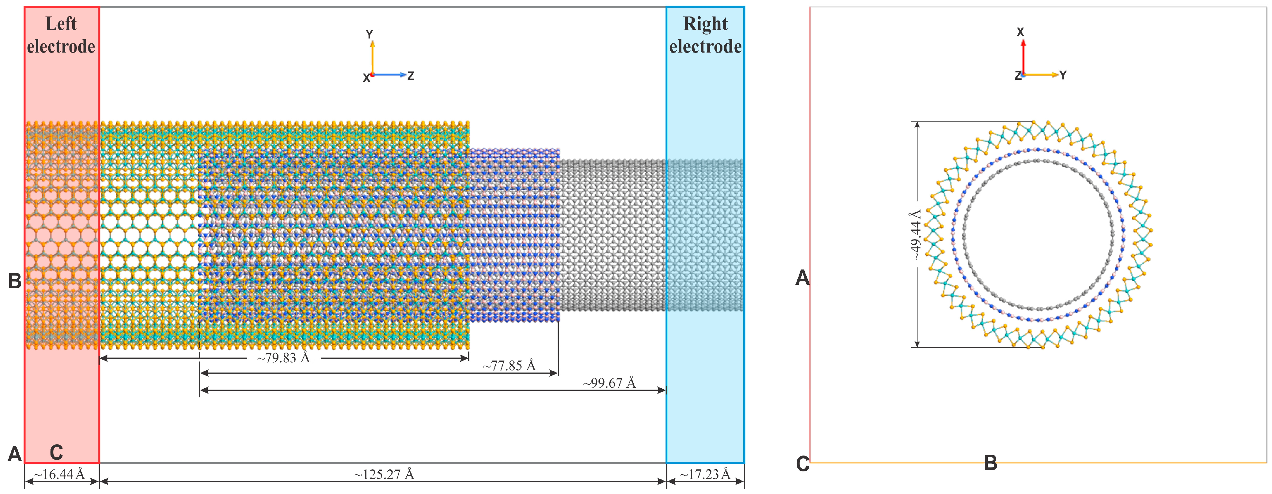
3. The Geometry of the Structures

The geometric parameters of the optimized MoX2(24,24) nanotubes (where X = S, Se, Te) are presented in Table 1. The diameter of an armchair (n,n) nanotube is calculated using the well-known formula:
d = a 3 n π ,
where a is the lattice constant, and n is the chirality index. Taking the graphene lattice constant of the CNT(24,24) a = 0.246 nm, its diameter is estimated to be approximately 3.28 nm. Similarly, the estimated diameters for hBN(24,24) and MoS2(24,24) are ≈3.77 nm and ≈4.18 nm, respectively. However, after the geometry optimization, the geometry optimization and the description of interatomic interactions were performed within the framework of DFT, using the generalized gradient approximation (GGA-PBE) as the exchange–correlation functional [73]. The optimization was carried out with force and stress thresholds of 0.02 eV/Å and 0.001 eV/Å3, respectively. A plane-wave cutoff energy of 360 Ry was used for the real-space grid during optimization.
As is known, typical 1D vdW heterodevices consist of telescopically nested nanotubes with diameters ranging from 1 nm to 5 nm and exhibiting various types of electronic conductivity [48]. It is experimentally challenging to manipulate nanotubes with small diameters; therefore, in this study, nanotubes with diameters closer to 5 nm were selected. The most suitable combinations for the coaxial vdW coupling, enabling the formation of 1D vdW heterostructures, are as follows (see Figure 1, Figure 2 and Figure 3):
  • MoS2(24,24) + hBN(27,27) + CNT(24,24) CNT(24,24)@ hBN(27,27)@MoS2(24,24);
  • MoSe2(24,24) + hBN(27,27) + CNT(24,24) CNT(24,24)@ hBN(27,27)@MoSe2(24,24);
  • MoTe2(24,24) + hBN(27,27) + CNT(24,24) CNT(24,24)@ hBN(27,27)@MoTe2(24,24).
These nanotubes possess compatible diameters for intercalating a CNT(24,24) nanotube (with a diameter of 31.23 Å) into larger-diameter TMD nanotubes MoX2(24,24), enabling the formation of 1D vdW nanoheterostructures. The individual nanotubes are separated by an insulating layer—an hBN(27,27) nanotube of a matching size. MoX2(24,24) nanotubes represent a complex three-layer structure, characterized by an inner diameter (D1) and an outer diameter (D2), as shown in Table 1 and Figure 1, Figure 2 and Figure 3. For example, the outer diameter D2 of the MoS2(24,24) nanotube is 46.79 Å, while its inner diameter D1 is 40.3 Å.
It is well known that one of the simplest topological defects found in graphene-like 2D materials is the SW defect [74,75]. This defect forms through a simple 90° rotation of a C–C bond (SW transformation), which disrupts the symmetry of the hexagonal graphene lattice, leading to the formation of two pentagons and two heptagons within the structure (see Figure 4). SW defects typically arise either during high-temperature annealing at the synthesis stage or as a result of irradiation. In [76,77], the dynamics of the SW defect in real time were investigated experimentally. The SW defect acts as an adsorption center for various atoms and molecules (e.g., [78]) and significantly affects the structural properties of graphene, promoting the formation of stable “ridges” due to the compressive strain generated in its interior region [79]. These structures can serve as quantum dots in graphene-based nanoelectronics. In addition, such defects can be used to “tune” the electronic band structure of graphene, making it more suitable for applications in graphene transistors. In our earlier work [65], we investigated the electronic properties of SW-defective graphene structures, revealing features in the density of states of graphene nanostructures—specifically, a defect band ~0.5 eV above the Fermi level, which serves as an identifier of the SW defect presence and concentration in such structures. Similar SW defects are also found in CNTs [80]. In [66], using DFT, we modeled the key electronic characteristics of SW-defective CNTs on the example of the CNT(9,0), showing that two interconnected longitudinal SW defects significantly alter the conductivity of the nanosystem. Naturally, it is of interest to examine how SW defects in the CNT(24,24) influence the electrical properties of the vdW heterostructures shown in Figure 1, Figure 2 and Figure 3. In this work, we studied the impact of both a single SW defect and a pair of connected longitudinal SW defects (see Figure 4 and Figure 5) on the electronic properties of vdW heterostructures. As in graphene, the presence of SW defects in CNTs leads to the formation of stable ridgelike features resembling quantum dots, arising from the compressive strain in the nanotube body (Figure 4 and Figure 5). It should be noted that the formation of SW defects in TMD structures is energetically unfavorable due to the polar nature of the chemical bonds between different atoms. However, a related effect resembling the SW defect is observed in the form of a “trifoliate” structure, resulting from a 60° rotation of the Mo–X bond [81,82].
Another fundamental type of defect in the structure of CNTs is the vacancy defect (see Figure 6). In [83], the correlation between electrical properties and the vacancy density in monolayer CNTs was investigated, along with the dependence of the vacancy influence range on the nanotube’s chirality. The study also examined band structure fluctuations induced by nanotube deformation. In [84] it was further shown that both the geometry of the CNT and the presence of different types of vacancy defects can significantly affect its properties. Thus, the influence of structural imperfections in CNTs on the transport properties of 1D vdW heterostructures based on the MoX2 (X = chalcogen)–hBN–CNT is of considerable interest.

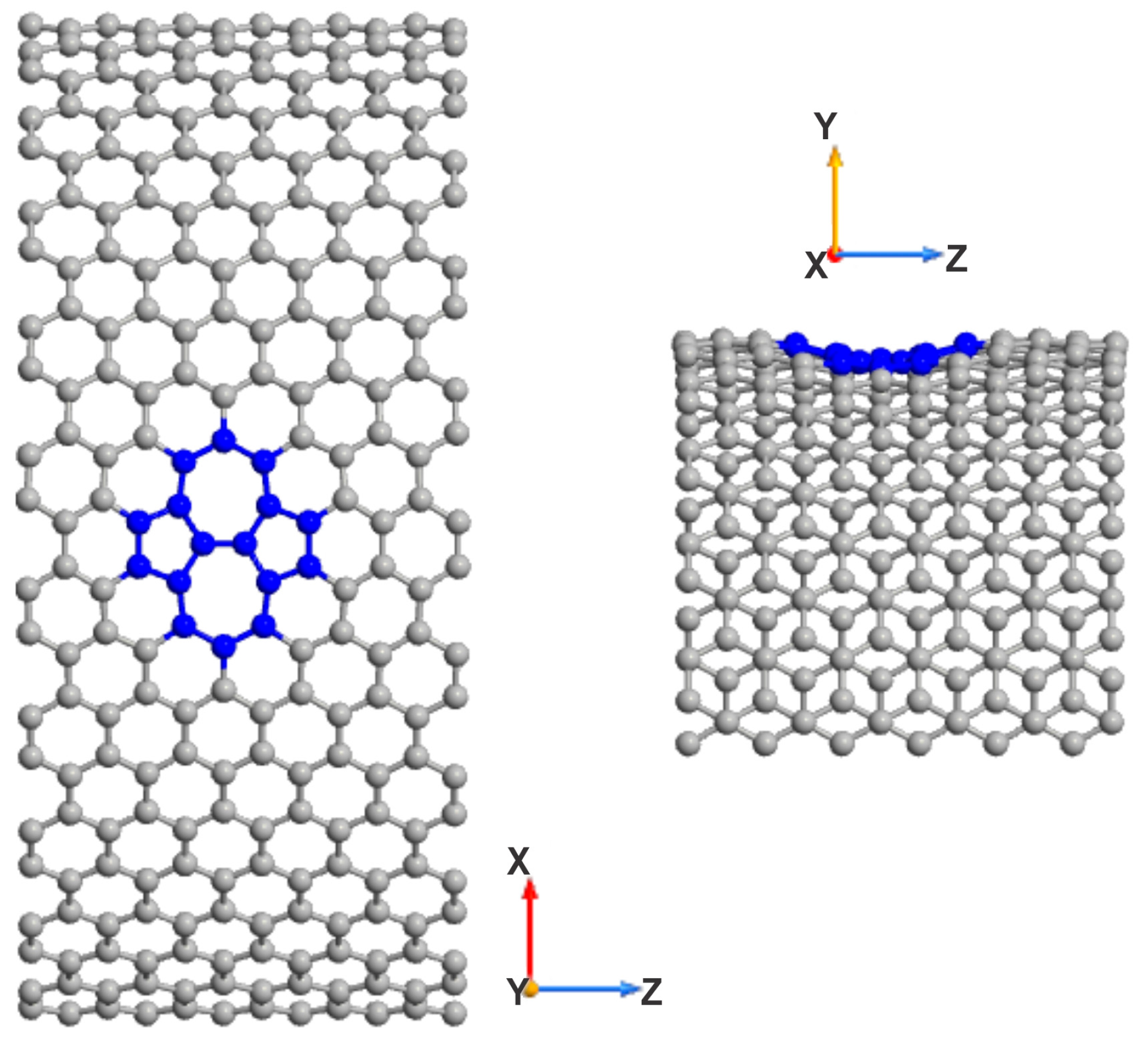
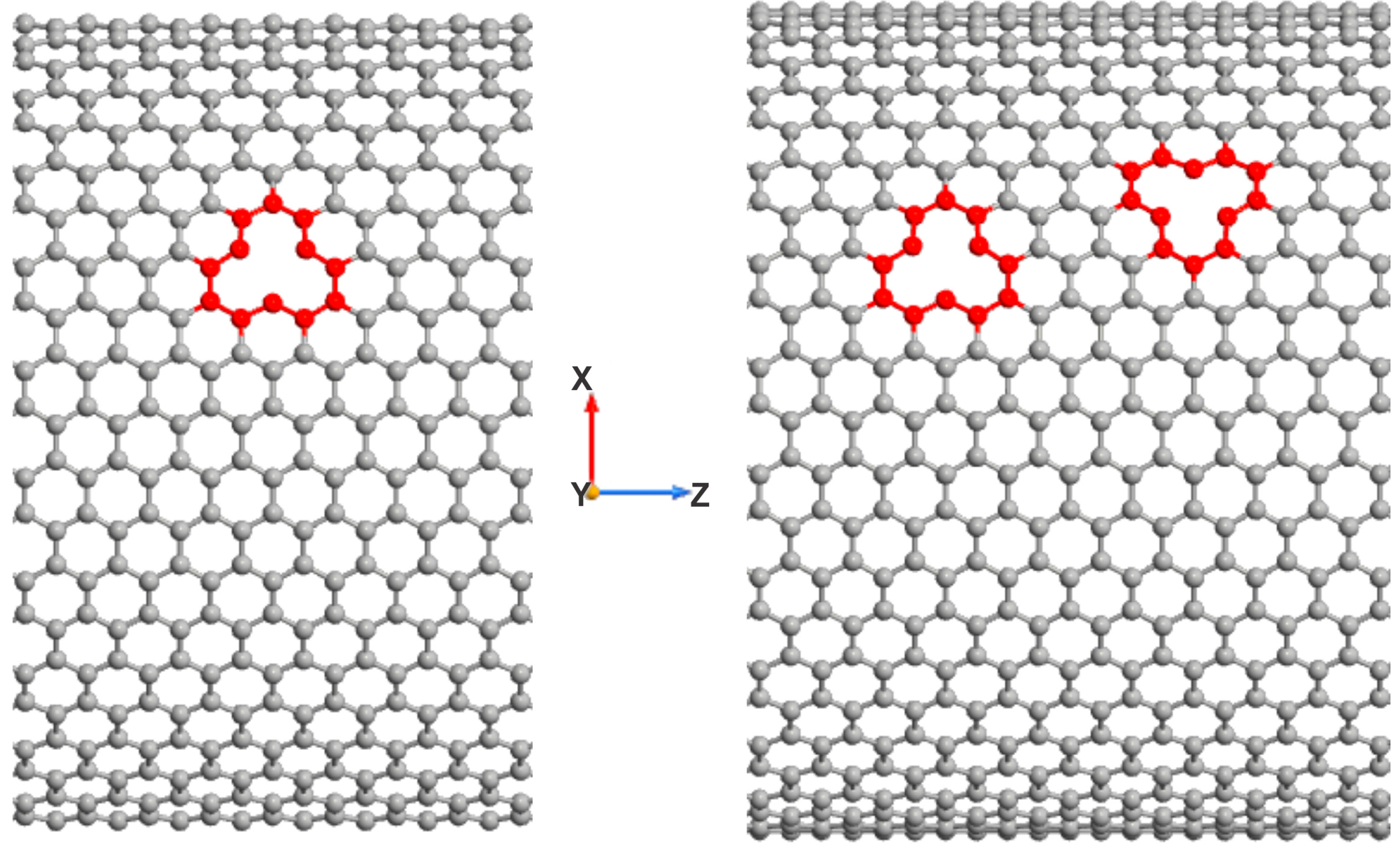
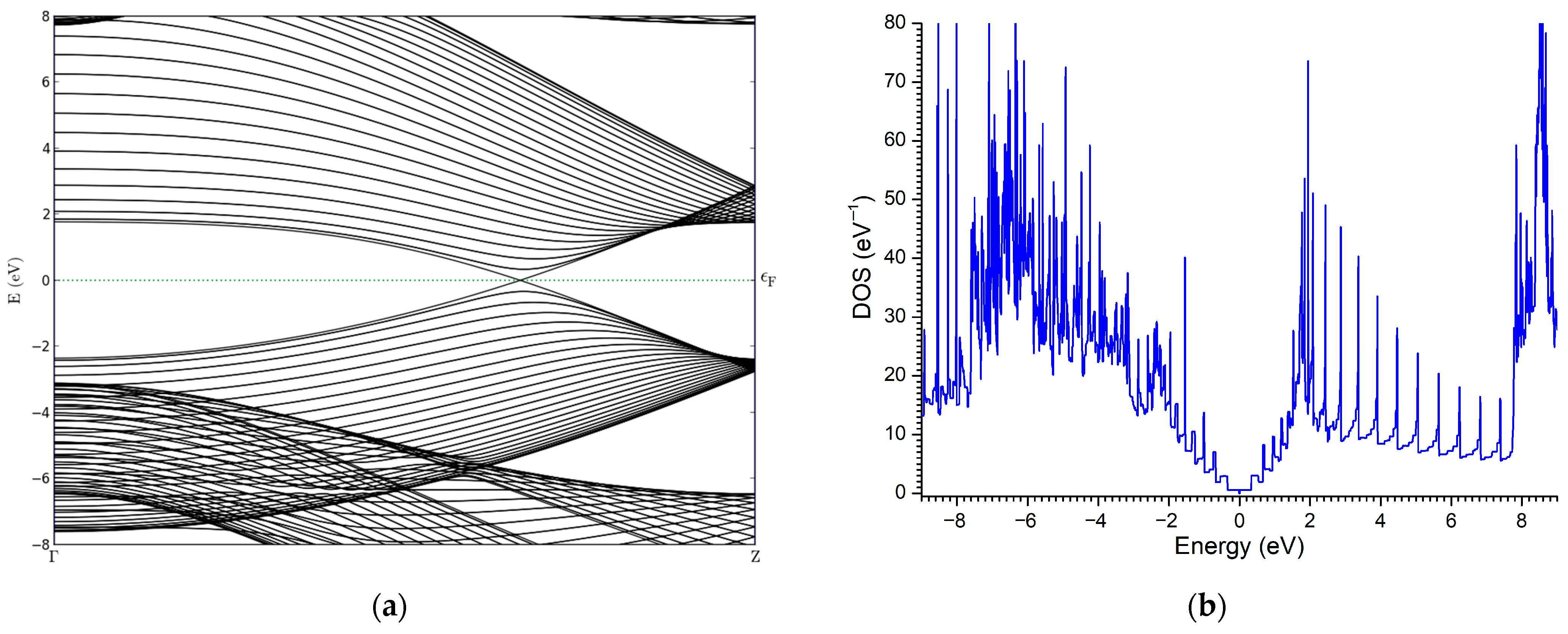
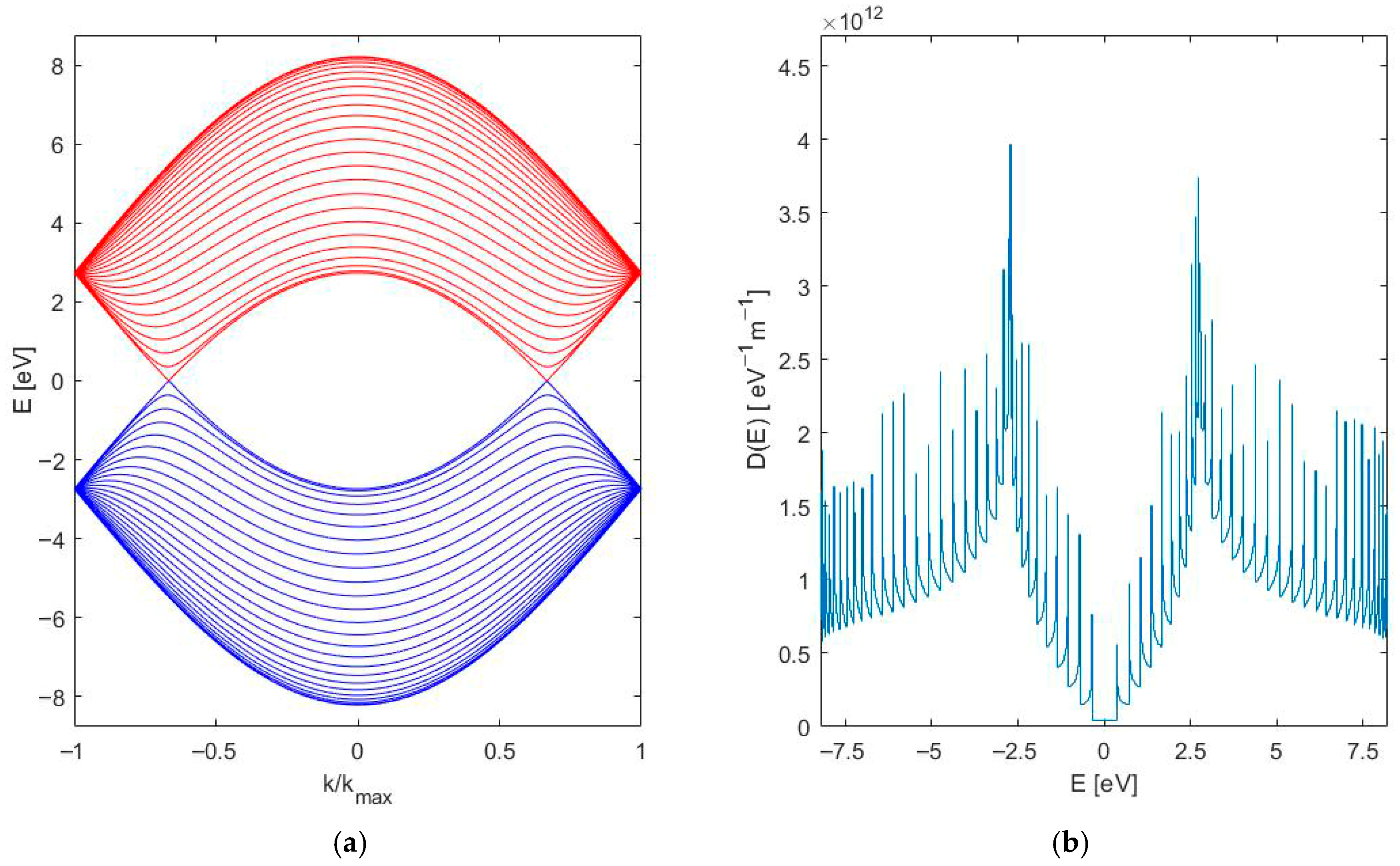
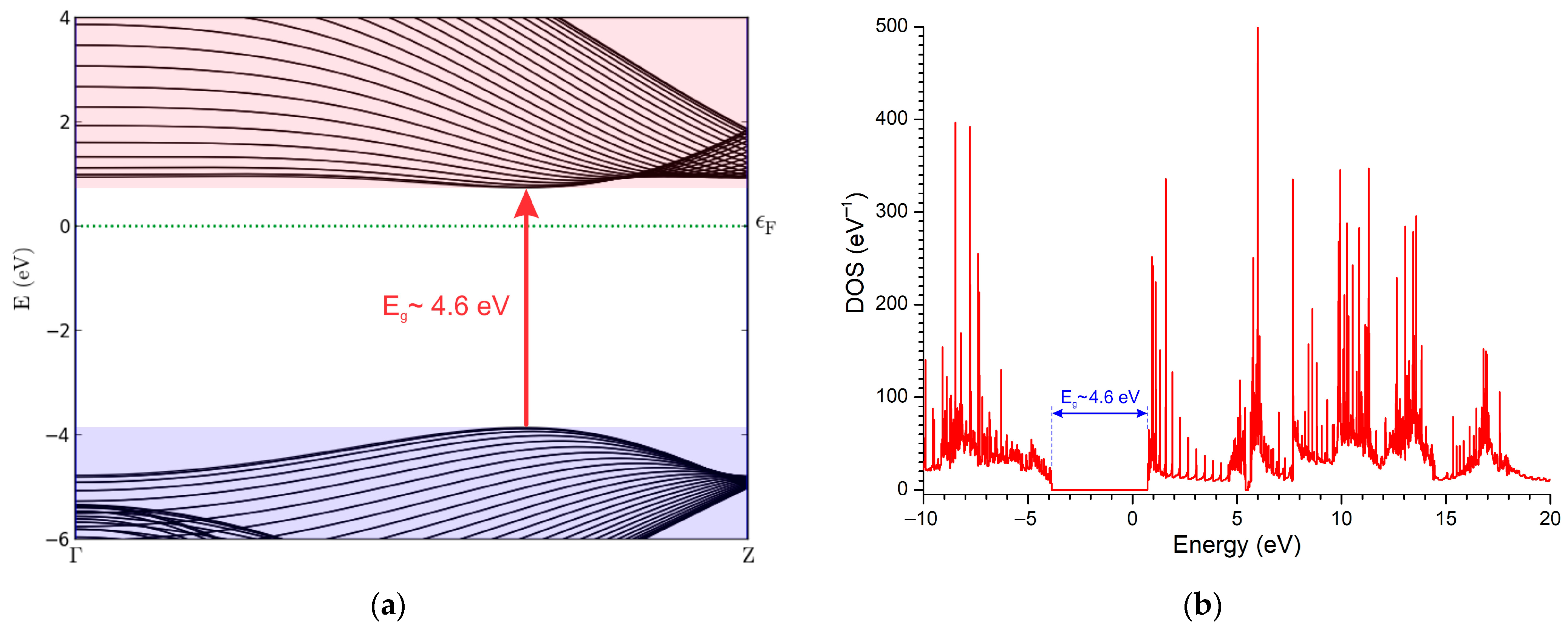
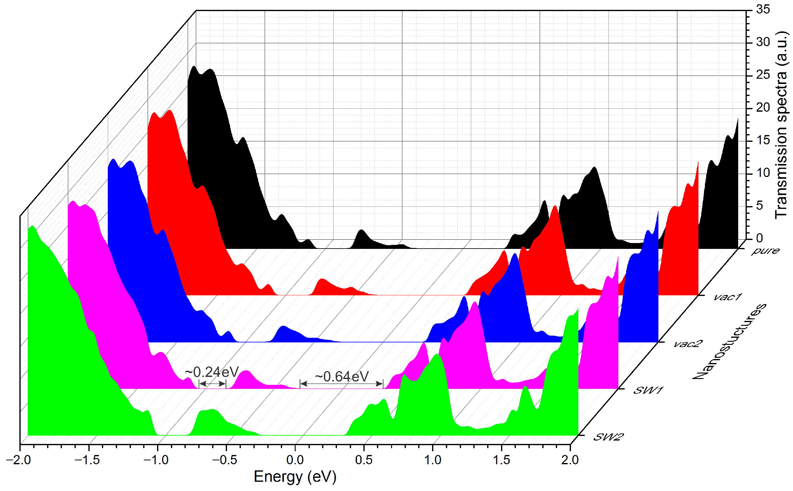
4. Results and Discussion

To provide a more detailed analysis of the transport characteristics, we first consider the electronic properties of the individual components. For easier manipulation and future device integration, nanotubes with relatively large diameters were selected. The band structure and density of states (DOS) of the CNT(24,24), calculated using DFT and a numerical method described in [85], are shown in Figure 7 and Figure 8. The results demonstrate a good agreement. As observed, the CNT(24,24) behaves as a conductor due to the absence of a band gap. Its band structure crosses the Fermi level, enabling free electron transport.
The band structure and DOS of hBN(27,27), calculated using DFT, are shown in Figure 9. Generally, large nanotubes such as(27,27) preserve the properties of the bulk material. However, the band gap of hBN(27,27), based on our calculations, is approximately 4.6 eV, which is narrower than the ~5.9 eV band gap of its 2D counterpart [6]. Nevertheless, hBN(27,27) retains its dielectric properties and can be effectively used as an insulating layer in nanoscale devices, particularly in 1D architectures.
The third component of the proposed nanodevice is a nanotube based on molybdenum dichalcogenides (MoX2) with a chirality index of n = m = 24. In our previous work [86], we demonstrated that increasing the diameter of the armchair MoS2(n,n) and MoSe2(n,n) nanotubes leads to an increase in their band gaps, approaching the band gap values of their 2D counterparts. We also found that single-walled MoS2 and MoSe2 nanotubes of the armchair type are indirect band gap semiconductors (with the exception of MoSe2(16,16), which has a direct band gap of 1.216 eV), whereas zigzag (n,0) nanotubes tend to have direct band gaps at the Γ point. The calculated band structures of MoX2(24,24) along the high-symmetry Γ–Z direction in the Brillouin zone are shown in Figure 10. As can be seen, MoTe2(24,24) exhibits a band gap of ~1.0 eV, which is significantly narrower than those of MoS2(24,24) (~1.5 eV) and MoSe2(24,24) (~1.27 eV). This is attributed to the larger atomic radii of Te and Se compared to S, which weakens interatomic bonding and lowers the band edge energies. Although monolayers of MoS2 and MoTe2 possess direct band gaps, their 1D analogs transition to indirect band gaps (see Figure 10a,c). The band structure of MoSe2 nanotubes with higher chirality indices differs from their MoS2 and MoTe2 counterparts. In large-diameter nanotubes, such as MoSe2(24,24), a transition toward a direct band gap may be induced—similarly to the case of MoSe2(16,16) [86]. It is worth noting that bilayer MoSe2 also exhibits a direct band gap, unlike its analogs which retain an indirect one [87].
Let us now examine the calculated transmission spectrum of the 1D vdW heterostructure MoS2(24,24)–hBN(27,27)–CNT(24,24) at a zero bias voltage, obtained using Equation (1) (Figure 11). As shown, the presence of vacancy defects significantly degrades the quasiparticle transport (curves vac1 and vac2) compared to SW defects. Naturally, the probability of quasiparticle transmission is highest in the defect-free device; however, the appearance of two coupled longitudinal SW defects in the CNT structure has a relatively minor effect on transport properties compared to other types of defects. It is known that increasing the vacancy concentration leads to an enlargement of the band gap in single-walled CNTs. For metallic CNTs, this can cause a transition from metallic to semimetallic behavior [88], whereas such a transition does not occur in semiconducting CNTs. In [89], it was shown that a single vacancy defect in the channel of a narrow-diameter metallic CNT can reduce its conductivity by a factor of two, and the presence of multiple vacancies can drastically degrade the conductance even further.
In the MoS2(24,24)–hBN(27,27)–CNT(24,24) heterostructure, the quasiparticle transport is blocked in the energy range of approximately −0.42 to 0.42 eV, forming a HOMO–LUMO gap of ~0.84 eV. The presence of the considered defects does not significantly affect this gap value.
Features of the transmission spectrum are reflected in the CVC, calculated using Equation (2). The CVC exhibits typical tunneling behavior, well described by the exponential dependence (Figure 12a). In a relatively broad bias voltage range (~−0.9 V to 0.9 V), no current flows through the heterodevice. The differential conductance, dI/dV, reveals more details (Figure 12b). As seen, the conductance profile resembles that of a two-mode phonon system with symmetric thermal behavior [90,91]. In such nanosystems, the conductance can increase or decrease due to phonon scattering. As shown earlier, MoS2(24,24) is an indirect band gap semiconductor (Figure 10a). In these types of semiconductors, quasiparticles require phonon participation to facilitate momentum change during transitions between bands (as the conduction band minimum and valence band maximum are located at different points in momentum space). Consequently, the tunneling probability is low, as it relies on the involvement of a third particle—a phonon. It is known that the tunneling probability increases with the temperature due to the greater phonon population.
It is also known that nanostructures containing correlated defects can form quantum dots or barriers, facilitating quasiparticle tunneling. In our case, resonant tunneling is manifested as a negative differential resistance (NDR) in the CVC (Figure 12, curves vac2, SW2). In these vdW heterostructures, at Vbias ≈ 1.85 V and 1.93 V, quasiparticles fall into allowed energy levels. However, in other structures, resonant tunneling is absent. Our hypothesis regarding this behavior will be discussed after analyzing the transport characteristics of the MoTe2(24,24)–hBN(27,27)–CNT(24,24) heterostructure. The high electrical conductivity of MoS2(24,24)-based nanostructures under the reverse bias, reaching approximately 1.3 × 10² μS at −2 V, significantly exceeds their conductivity under the forward bias (Figure 12). This indicates that such nanostructures efficiently conduct the electric current under a negative bias voltage, in contrast to a positive bias. This characteristic enables their potential use as back nanodiodes. However, the presence of point defects severely degrades the rectifying behavior of these nanostructures: while defect-free nanostructures allow a current up to 76 μA at −2 V, the presence of various point defects reduces the current to ~−39 to −48 μA, depending on the defect type (Figure 12).
A similar behavior is observed in the MoTe2(24,24)–hBN(27,27)–CNT(24,24) heterostructure. As seen from the transmission spectrum, the quasiparticle transport is blocked in the energy range of approximately −0.34 to 0.3 eV (Figure 13). The HOMO–LUMO gap is ~0.64 eV. Additionally, in the bias range of ~−1.07 to 0.83 eV, the device does not allow quasiparticle transmission.
The nanosystem predominantly conducts the current in the forward bias direction, while under the reverse bias the current decreases by a factor of approximately 1.7 (Figure 14). For example, in the defect-free structure, the maximum current under the forward bias reaches ~46 μA, whereas under the reverse bias it is reduced to ~26 μA (Figure 14a, curve pure). This rectifying behavior enables the use of such devices for current modulation in nanoscale circuits [92,93]; i.e., this property allows them to be used as nanodiodes.
Distinct peaks in the dI/dV spectrum emerge at bias voltages of approximately −1.3 V, 1.1 V, and 1.53 V. In the structure with two SW defects, several spectral features shift and appear at −1.4 V and 1.7 V (Figure 14b). The presence of coupled SW defects increases the current in both forward and reverse bias conditions. We suggest that in this case, ordered pentagon–heptagon pairs may act as tunable “conductive channels”. Moreover, the charge carrier mobility in MoTe2 is higher than in MoS2 and MoSe2 due to the smaller effective electron mass. This likely explains the enhanced conductivity of the MoTe2-based vdW heterostructure compared to others. Similarly to the previous nanosystem, the dI/dV spectrum exhibits the shape of a two-mode phonon system. In [94], interference effects are discussed as one of the possible mechanisms responsible for the emergence of negative differential resistance (NDR). However, such interference—as a resonance phenomenon—can be suppressed by electron–phonon scattering. In our case, we assume that the absence of pronounced resonant effects in the transport characteristics of MoS2- and MoTe2-based nanodevices is due to the suppression of resonant tunneling by the electron–phonon interaction. Both materials are indirect band gap semiconductors (see Figure 11), which underscores the key role of phonons in quasiparticle transport.
A different behavior is observed in the 1D vdW heterostructure, MoSe2(24,24)–hBN(27,27)–CNT(24,24). The calculated transmission spectrum of this heterostructure, including the previously considered defects, is shown in Figure 15. It can be seen that in the energy range of approximately −0.4 to 0.4 eV, the device blocks quasiparticle transport, forming a HOMO–LUMO gap of ~0.8 eV. Additional transmission suppression occurs in the ranges of ~−1.9 to −1.1 eV and ~1.34 to 1.58 eV. Compared to the transmission spectra of other nanosystems, this system exhibits a noticeable series of sharp peak structures, which is indicative of pronounced resonant effects.
The calculated CVC and differential conductance for this system are presented in Figure 16a and16b, respectively. The CVC of the given nanostructure resembles that of a double tunnel barrier with a quantum-sized central region. To facilitate the explanation of the I–V behavior, its corresponding energy band diagram is presented in Figure 17. The ordinate represents the quasiparticle energy, while the abscissa denotes the spatial coordinate. In the energy diagram, the cathode and anode electrodes are labeled as 1 (blue) and 5 (red), respectively, with their corresponding Fermi levels, E F 1 and E F 5 , indicated. Regions 2 and 4 (green) represent the tunnel barriers, and region 3 (yellow) corresponds to the quantum-confined region. It is important to note that the electric potential applied between the cathode (1) and anode (5) drops across tunnel barriers 2 and 4, which is approximately equally distributed. As a result, the potential energy of quasiparticles in the anode region decreases by a certain amount e V , which causes a downward shift in all energy levels (Figure 17). In the quantum-confined region (3), the potential energy of electrons decreases by an amount of e V 2 . Consequently, the allowed energy levels E 1 and E 2 also shift downward by the same amount. The upper part of the energy diagram corresponds to the case when e V 2 < Δ 1 , and here Δ 1 denotes the energy difference between the allowed levels in the quantum-confined region and the Fermi level ε 1 , 2 ε F . Under this condition, most quasiparticles from region 1 near the Fermi level E F 1 do not find available energy levels in region 3. As a result, their tunneling through barrier 2 does not occur, and the tunnel current remains negligible.
When the voltage between the anode and the cathode increases to a value at which e V 2 Δ 1 , a significant portion of quasiparticles with energies near the Fermi level E F 1 gain the ability to overcome tunnel barrier 2. In this case, under the forward bias, the electric current through the nanostructure rises sharply, reaching its maximum value when V 1 = 2 Δ 1 e . Depending on the presence and type of defects, V 1 varies between 1.21 V and 1.58 V. When the applied voltage exceeds V 1 , quasiparticles can no longer access available energy states beyond the tunneling barrier, and the current flow is suppressed. A decrease in the tunneling current to V 2 = 2 Δ 2 e is observed until a new allowed energy level ε 2 becomes accessible at V 2 , and so the tunnel current starts to increase again. Here Δ 2 = ε 2 ε F (Figure 17). The value of V 2 ranges from 1.74 V to 1.79 V, depending on the defect configuration. This nanostructure exhibits distinct behavior compared to others previously discussed: the CVC shows two NDR (negative differential resistance) regions, and the corresponding dI/dV spectrum displays two bands (Figure 16b, marked in yellow and orange). It is noteworthy that the differential conductance of the heterostructures with SW defects is higher than in other configurations, reaching 26–27 μS (Figure 16b, indicated with arrows). We assume that this is due to resonant interactions between the SW defects, which result in conductance peaks at specific voltages. Under the reverse bias, at Vbias ≈ −1 V, the leakage current is approximately −0.5 to −0.75 μA. With a pair of SW defects, the leakage current increases significantly to −1.7 μA—is almost three times higher than with simpler defects. These features are also reflected in the dI/dV spectrum: the differential conductance near −1 V increases from −3 to −4 μS, and in the presence of paired SW defects, it reaches −12 μS. Previous studies [95,96,97] have shown that the NDR typically appears only under one polarity of the applied voltage, depending on the symmetry of the nanostructure [98]. In our case, the primary NDR peak is observed under the positive bias, which is likely due to the asymmetric structure of the vdW heterostructure relative to the Z-axis (see Figure 1, Figure 2 and Figure 3).
As shown above, electron tunneling in semiconductors strongly depends on the nature of the band gap (direct or indirect). The tunneling mechanisms in indirect band gap semiconductors were discussed in detail for MoS2(24,24)- and MoTe2(24,24)-based heterostructures. In direct band gap semiconductors, quasiparticles tunnel between the valence and conduction bands without requiring a change in momentum, as the conduction band minimum and valence band maximum are located at the same point in momentum space. This results in a high tunneling probability due to momentum conservation. We suggest that this is the reason why pronounced resonant effects are observed in the MoSe2-based nanodevices. Their transport properties make them promising candidates for applications as high-speed switching tunnel nanodiodes.

5. Conclusions

In this study, the electronic properties of 1D vdW nanoheterodevices based on the MoX2–hBN–CNT were investigated within the framework of DFT. The following original findings were obtained:
– It was revealed that in MoS2(24,24)- and MoTe2(24,24)-based heterodevices, interference as a resonant phenomenon is suppressed by electron–phonon scattering. Since these are indirect band gap semiconductors, phonon participation is required for quasiparticles to change momentum during interband transitions, resulting in a reduced tunneling probability.
– It was found that MoSe2(24,24)-based heterodevices exhibit resonant tunneling, as they are direct band gap semiconductors. In such systems, quasiparticles tunnel between the valence and conduction bands without momentum change, which leads to a high tunneling probability. The observed transport characteristics make these structures promising candidates for high-speed tunnel nanodiodes.
– It was demonstrated that vacancy defects in the studied 1D nanoheterostructures significantly degrade the quasiparticle transport compared to SW defects. This is presumably due to the reduced charge carrier mobility caused by vacancy defects in the CNT structure.
– It was shown that the presence of complex vacancy and SW defects in the MoS2(24,24)-based heterostructure forms potential barriers that facilitate quasiparticle tunneling at bias voltages of approximately 1.85 V and 1.93 V, respectively.
– It was identified that the conductance of MoTe2(24,24)-based heterostructures with SW defects is higher than that of other defect-containing heterostructures, reaching 26–27 μS. This behavior is attributed to resonant interactions between SW defects, which generate conductance peaks at specific voltages.
– It was shown that MoX2–hBN–CNT nanosystems predominantly conduct the current in the forward direction. Under the reverse bias, the current decreases by a factor of approximately 1.7. For the defect-free structure, the maximum forward current reaches ~46 μA, while under the reverse bias it is ~26 μA. This rectifying behavior indicates the potential of such heterostructures for current regulation in nanoscale circuits.
The results obtained in this study may prove useful for the design and modeling of next-generation nanoelectronic devices.

Author Contributions

Conceptualization, D.S., methodology, D.S. and K.S.; software, D.S.; validation, D.S. and K.S.; formal analysis, D.S. and K.S.; investigation, D.S. and K.S.; resources, D.S. and K.S.; data curation, D.S.; writing—original draft preparation, D.S.; writing—review and editing, D.S. and K.S.; visualization, D.S.; supervision, D.S.; project administration, D.S.; funding acquisition, D.S. All authors have read and agreed to the published version of the manuscript.

Funding

This research has been funded by the Science Committee of the Ministry of Science and Higher Education of the Republic of Kazakhstan (Grant No. AP23488734).

Data Availability Statement

The original contributions presented in this study are included in the article. Further inquiries can be directed to the corresponding authors.

Conflicts of Interest

The authors declare no conflicts of interest.

References

  1. Novoselov, K.S.; Geim, A.K.; Morozov, S.V.; Jiang, D.; Zhang, Y.; Dubonos, S.V.; Grigorieva, I.V.; Firsov, A.A. Electric field effect in atomically thin carbon films. Science 2004, 306, 666–669. [Google Scholar] [CrossRef] [PubMed]
  2. Farjadian, F.; Abbaspour, S.; Sadatlu, M.A.A.; Mirkiani, S.; Ghasemi, A.; Hoseini-Ghahfarokhi, M.; Mozaffari, N.; Karimi, M.; Hamblin, M.R. Recent Developments in Graphene and Graphene Oxide: Properties, Synthesis, and Modifications: A Review. Chemistryselect 2020, 5, 10200–10219. [Google Scholar] [CrossRef]
  3. Mogera, U.; Kulkarni, G.U. A new twist in graphene research: Twisted graphene. Carbon 2020, 156, 470–487. [Google Scholar] [CrossRef]
  4. Fiore, S.; Klinkert, C.; Ducry, F.; Backman, J.; Luisier, M. Influence of the hBN Dielectric Layers on the Quantum Transport Properties of MoS2 Transistors. Materials 2022, 15, 1062. [Google Scholar] [CrossRef] [PubMed]
  5. Delgado, N.; Salas, O.; Garcés, E.; Magaña, L.F. Ab-Initio Calculation of the Electrical Conductivity, Optical Absorption, and Reflectivity of the 2D Materials SnC and NbC. Crystals 2023, 13, 682. [Google Scholar] [CrossRef]
  6. Vandenberghe, W.G.; Osanloo, M.R. Two-Dimensional Dielectrics for Future Electronics: Hexagonal Boron Nitride, Oxyhalides, Transition-Metal Nitride Halides, and Beyond. ACS Appl. Electron. Mater. 2023, 5, 623–631. [Google Scholar] [CrossRef]
  7. Sergeyev, D.; Ashikov, N.; Zhanturina, N. Electric Transport Properties of a Model NanojunctionGraphene–Fullerene C60–Graphene. Int. J. Nanosci. 2021, 20, 2150007. [Google Scholar] [CrossRef]
  8. Geim, A.K.; Grigorieva, I.V. Van der Waals heterostructures. Nature 2013, 499, 419–425. [Google Scholar] [CrossRef] [PubMed]
  9. Luo, H.; Wang, B.; Wang, E.; Wang, X.; Sun, Y.; Liu, K. High-Responsivity Photovoltaic Photodetectors Based on MoTe2/MoSe2 van der Waals Heterojunctions. Crystals 2019, 9, 315. [Google Scholar] [CrossRef]
  10. Molaei, M.J.; Younas, M.; Rezakazemi, M. Van der Waals heterostructures in ultrathin 2D solar cells: State-of-the-art review. Mater. Sci. Eng. B 2022, 285, 115936. [Google Scholar] [CrossRef]
  11. Li, X.; Yuan, P.; He, M.; Li, L.; Du, J.; Xiong, W.; Xia, C.; Kou, L. Optoelectronic properties and applications of two-dimensional layered semiconductor van der Waals heterostructures: Perspective from theory. J. Phys. Condens. Matter 2023, 35, 043001. [Google Scholar] [CrossRef] [PubMed]
  12. Xu, H.; Xue, Y.; Liu, Z.; Tang, Q.; Wang, T.; Gao, X.; Qi, Y.; Chen, Y.P.; Ma, C.; Jiang, Y. Van der Waals Heterostructures for Photoelectric, Memory, and Neural Network Applications. Small Sci. 2024, 4, 300213. [Google Scholar] [CrossRef] [PubMed]
  13. Li, X.X.; Sha, X.Z.; Zhang, T.Y.; Wang, H.W.; Han, Z.V. The Emerging Nano-Opto-Electromechanical Systems Based on van der Waals Heterostructures. Adv. Funct. Mater. 2025; early access. [Google Scholar] [CrossRef]
  14. Petrov, A.V.; Ivanov-Schitz, A.K.; Murin, I.V. Enhanced Oxygen Mobility in Undoped ZrO2-CeO2 Heterostructure. Phys. Status Solidi A 2023, 220, 2200494. [Google Scholar] [CrossRef]
  15. Davletshin, A.R.; Ustiuzhanina, S.V.; Kistanov, A.A.; Saadatmand, D.; Dmitriev, S.V.; Zhou, K.; Korznikova, E.A. Electronic structure of graphene- and BN-supported phosphorene. Phys. B Condens. Matter 2018, 534, 63–67. [Google Scholar] [CrossRef]
  16. Li, X.H.; Wang, B.J.; Ke, S.H. Blue phosphorene/MoSi2N4 van der Waals type-II heterostructure: Highly efficient bifunctional materials for photocatalytics and photovoltaics. Chin. Phys. B 2023, 32, 027104. [Google Scholar] [CrossRef]
  17. Sergeyev, D. Single electron transistor based on endohedralmetallofullerenes Me@C60 (Me = Li, Na, K). J. Nano- Electron. Phys. 2020, 12, 03017. [Google Scholar] [CrossRef] [PubMed]
  18. Darsey, J.A. Artificial Intelligence Modeling of Materials’ Bulk Chemical and Physical Properties. Crystals 2024, 14, 866. [Google Scholar] [CrossRef]
  19. Park, H.K.; Kim, Y.; Park, J.M.; Ameyama, K.; Kim, H.S. Efficient design of harmonic structure using an integrated hetero-deformation induced hardening model and machine learning algorithm. Acta Mater. 2023, 244, 118583. [Google Scholar] [CrossRef]
  20. Zheng, Y.; Kumamoto, A.; Hisama, K.; Otsuka, K.; Wickerson, G.; Sato, Y.; Liu, M.; Inoue, T.; Chiashi, S.; Tang, D.-M.; et al. One-dimensional van der Waals heterostructures: Growth mechanism and handedness correlation revealed by nondestructive TEM. Proc. Natl. Acad. Sci. USA 2021, 118, e2107295118. [Google Scholar] [CrossRef] [PubMed]
  21. Fei, R.; Li, W.; Li, J.; Yang, L. Giant piezoelectricity of monolayer group IV monochalcogenides: SnSe, SnS, GeSe, and GeS. Appl. Phys. Lett. 2015, 107, 173104. [Google Scholar] [CrossRef]
  22. Artyukhov, V.I.; Gupta, S.; Kutana, A.; Yakobson, B.I. Flexoelectricity and charge separation in carbon nanotubes. Nano Lett. 2020, 20, 3240–3246. [Google Scholar] [CrossRef] [PubMed]
  23. Lu, A.Y.; Zhu, H.; Xiao, J.; Chuu, C.P.; Han, Y.M.; Chiu, M.H.; Cheng, C.C.; Yang, C.W.; Wei, K.H.; Yang, Y.; et al. Janus monolayers of transition metal dichalcogenides. Nat. Nanotech. 2017, 12, 744–749. [Google Scholar] [CrossRef] [PubMed]
  24. Lee, C.; Rathi, S.; Khan, M.A.; Lim, D.; Kim, Y.; Yun, S.J.; Youn, D.H.; Watanabe, K.; Taniguchi, T.; Kim, G.H. Comparison of trapped charges and hysteresis behavior in hBN encapsulated single MoS2 flake based field effect transistors on SiO2 and hBN substrates. Nanotechnology 2018, 29, 335202. [Google Scholar] [CrossRef] [PubMed]
  25. Illarionov, Y.Y.; Knobloch, T.; Jech, M.; Lanza, M.; Akinwande, D.; Vexler, M.I.; Mueller, T.; Lemme, M.C.; Fiori, G.; Schwierz, F.; et al. Insulators for 2D nanoelectronics: The gap to bridge. Nat. Commun. 2020, 11, 3385. [Google Scholar] [CrossRef] [PubMed]
  26. Illarionov, Y.; Banshchikov, A.G.; Polyushkin, D.K.; Wachter, S.; Knobloch, T.; Thesberg, M.; Mennel, L.; Paur, M.; Stöger-Pollach, M.; Steiger-Thirsfeld, A.; et al. Ultrathin calcium fluoride insulators for two-dimensional field-effect transistors. Nat. Electron. 2019, 2, 230–235. [Google Scholar] [CrossRef]
  27. She, A.X.; Zhao, Y.C.; Ni, J.; Dai, Z.H. The influence of lattice anharmonicity on the thermal transport properties of two-dimensional MgF2. J. Phys. D Appl. Phys. 2025, 58, 045305. [Google Scholar] [CrossRef]
  28. Chattopadhyay, S.; Mahapatra, P.L.; Mattur, M.N.; Pramanik, A.; Gupta, S.; Pieshkov, T.S.; Saju, S.; Costin, G.; Vajtai, R.; Tiwary, C.S.; et al. Unlocking the Potential: Atomically Thin 2D Fluoritene from Exfoliated Fluorite Ore and Its Electrochemical Activity. Nano Lett. 2024, 24, 7284–7292. [Google Scholar] [CrossRef] [PubMed]
  29. Li, Z.X.; Ren, Q.P.; Chang, Y.X.; Ding, D.S.; Ma, L.L.; Xu, Y.S.; Zhang, S.Q.; Zhang, X.H. 1D to 2D Growth of NaF Crystals in Photothermo-Refractive Glasses. Cryst. Growth Des. 2024, 24, 7981–7989. [Google Scholar] [CrossRef]
  30. Shunkeyev, K.; Tilep, A.; Sagimbayeva, S.; Ubaev, Z.; Lushchik, A. The Effect of Instability of KCl:Na Single Crystals. Crystals 2023, 13, 364. [Google Scholar] [CrossRef]
  31. Maestre, C.; Li, Y.D.; Garnier, V.; Steyer, P.; Roux, S.; Plaud, A.; Loiseau, A.; Barjon, J.; Ren, L.; Robert, C.; et al. From the synthesis of hBN crystals to their use as nanosheets in van der Waals heterostructures. 2D Mater. 2022, 9, 035008. [Google Scholar] [CrossRef]
  32. Gong, Y.; Xu, Z.-Q.; Li, D.; Zhang, J.; Aharonovich, I.; Zhang, Y. Two-Dimensional Hexagonal Boron Nitride for Building Next-Generation Energy-Efficient Devices. ACS Energy Lett. 2021, 6, 985–996. [Google Scholar] [CrossRef]
  33. Robertson, J. High dielectric constant oxides. Eur. Phys. 2004, 28, 265–291. [Google Scholar] [CrossRef]
  34. Li, W.; Zhou, J.; Cai, S.H.; Yu, Z.H.; Zhang, J.L.; Fang, N.; Li, T.; Wu, Y.; Chen, T.; Xie, X.; et al. Uniform and ultrathin high-κ gate dielectrics for two-dimensional electronic devices. Nat. Electron. 2019, 2, 563–571. [Google Scholar] [CrossRef]
  35. Illarionov, Y.; Waltl, M.; Rzepa, G.; Knobloch, T.; Kim, J.S.; Akinwande, D.; Grasser, T. Highly-stable black phosphorus field-effect transistors with low density of oxide traps. npj 2D Mater. Appl. 2017, 1, 23. [Google Scholar] [CrossRef]
  36. Xiang, R.; Inoue, T.; Zheng, Y.J.; Kumamoto, A.; Qian, Y.; Sato, Y.; Liu, M.; Tang, D.; Gokhale, D.; Guo, J.; et al. One-dimensional van der Waals heterostructures. Science 2020, 367, 537–542. [Google Scholar] [CrossRef] [PubMed]
  37. Baithi, M.; Duong, D.L. Doped, Two-Dimensional, Semiconducting Transition Metal Dichalcogenides in Low-Concentration Regime. Crystals 2024, 14, 832. [Google Scholar] [CrossRef]
  38. Moon, B.H. Metal-insulator transition in two-dimensional transition metal dichalcogenides. Emergent Mater. 2021, 4, 989–998. [Google Scholar] [CrossRef]
  39. Rasulov, V.R.; Rasulov, R.Y.; Nasirov, M.K.; Muminov, I.A.; Mamatova, M.M. Theory of size quantization in monolayers of transition metal dichalcogenides. Phys. Scr. 2024, 99, 105987. [Google Scholar] [CrossRef]
  40. Kim, Y.; Kim, J. Near-field optical imaging and spectroscopy of 2D-TMDs. Nanophotonics 2021, 10, 3397–3415. [Google Scholar] [CrossRef]
  41. Ding, D.D.; Qu, Z.Z.; Han, X.Y.; Han, C.R.; Zhuang, Q.; Yu, X.L.; Niu, R.R.; Wang, Z.Y.; Li, Z.X.; Gan, Z.Z.; et al. Multivalley Superconductivity in Monolayer Transition Metal Dichalcogenides. Nano Lett. 2022, 22, 7919–7926. [Google Scholar] [CrossRef] [PubMed]
  42. Heil, C.; Ponce, S.; Lambert, H.; Schlipf, M.; Margine, E.R.; Giustino, F. Origin of Superconductivity and Latent Charge Density Wave in NbS2. Phys. Rev. Lett. 2017, 119, 087003. [Google Scholar] [CrossRef] [PubMed]
  43. Tsuppayakorn-aek, P.; Pluengphon, P.; Phansuke, P.; Inceesungvorn, B.; Busayaporn, W.; Kaewtubtim, P.; Bovornratanaraks, T. Effect of substitution on the superconducting phase of transition metal dichalcogenideNb(SexS1-x)2 van der Waals layered structure. Sci. Rep. 2021, 11, 15215. [Google Scholar] [CrossRef] [PubMed]
  44. Sergeyev, D.M. Modeling of the transport properties of SNS contacts for strong electron-phonon interactions. Russ. Phys. J. 2016, 59, 456–465. [Google Scholar] [CrossRef]
  45. Sergeyev, D.; Shunkeyev, K.; Solovjov, A.L. On a model of a Josephson junction with a single quantum channel featuring a “deformed” Andreev reflection coefficient. Low Temp. Phys. 2024, 50, 976–981. [Google Scholar] [CrossRef]
  46. Chen, M.D.; Li, L.; Xu, M.Z.; Li, W.W.; Zheng, L.; Wang, X.W. Quasi-One-Dimensional van der Waals Transition Metal Trichalcogenides. Research 2023, 6, 0066. [Google Scholar] [CrossRef] [PubMed]
  47. Chin, H.T.; Hofmann, M.; Huang, S.Y.; Yao, S.F.; Lee, J.J.; Chen, C.C.; Ting, C.C.; Hsieh, Y.P. Ultra-thin 2D transition metal monochalcogenide crystals by planarized reactions. npj 2D Mater. Appl. 2021, 5, 28. [Google Scholar] [CrossRef]
  48. Xiang, R.; Maruyama, S.; Li, Y. Building blocks for one-dimensional van der Waals heterostructures. Natl. Sci. Open 2022, 1, 20220016. [Google Scholar] [CrossRef]
  49. Ratnikov, P.; Silin, A. Two-dimensional graphene electronics: Current status and prospects. Phys.-Usp. 2018, 61, 1139–1174. [Google Scholar] [CrossRef]
  50. Shah, S.J.; Chen, J.Y.; Xie, X.; Oyang, X.; Ouyang, F.P.; Liu, Z.W. Progress and prospects of Moiré superlattices in twisted TMD heterostructures. Nano Res. 2024, 17, 10134–10161. [Google Scholar] [CrossRef]
  51. Chuang, M.H.; Chen, C.A.; Liu, P.Y.; Zhang, X.Q.; Yeh, N.Y.; Shih, H.J.; Lee, Y.H. Scalable Moire Lattice with Oriented TMD Monolayers. Nanoscale Res. Lett. 2022, 17, 34. [Google Scholar] [CrossRef] [PubMed]
  52. Sergeyev, D.; Duisenova, A.; Solovjov, A.; Ismayilova, N. Electron transport in a stressed moiré bigraphene structure. Results Phys. 2023, 54, 107140. [Google Scholar] [CrossRef]
  53. Yankowitz, M.; Larentis, S.; Kim, K.; Xue, J.M.; McKenzie, D.; Huang, S.Q. Intrinsic Disorder in Graphene on Transition Metal DichalcogenideHeterostructures. Nano Lett. 2015, 15, 1925–1929. [Google Scholar] [CrossRef] [PubMed]
  54. Lee, H.Y.; Wang, Z.Y.; Chen, G.C.; Holtzman, L.N.; Yan, X.Z.; Amontree, J.; Zangiabadi, A.; Watanabe, K.; Taniguchi, T.; Barmak, K.; et al. In situ via Contact to hBN-Encapsulated Air-Sensitive Atomically Thin Semiconductors. ACS Nano 2024, 18, 17111–17118. [Google Scholar] [CrossRef] [PubMed]
  55. Lan, H.Y.; Tripathi, R.; Appenzeller, J.; Chen, Z.H. Near-Ideal Subthreshold Swing in Scaled 2D Transistors: The Critical Role of Monolayer hBN Passivation. IEEE Electr. Device Lett. 2024, 45, 1337–1340. [Google Scholar] [CrossRef]
  56. Kim, M.; Lee, Y.; Kumar, S.; Kang, D.; Lee, S.; Nguyen, V.; Nguyen, V.H.; Nguyen, D.C.; Jaffery, S.H.A.; Jung, J.; et al. UV light controlled optoelectronic memory based on WSe2 and hBN encapsulated grapheneheterostructures. J. Alloy. Compd. 2023, 936, 168333. [Google Scholar] [CrossRef]
  57. Su, Z.; Zhao, Y.; Huang, Y.; Xu, C.; Yang, X.; Wang, B.; Xu, B.; Xu, S.; Bai, G. Light-driven soft actuator based on graphene and WSe2 nanosheets composite for multimodal motion and remote manipulation. Nano Res. 2023, 16, 1313–1319. [Google Scholar] [CrossRef]
  58. Li, C.; Xu, Z.Q.; Mendelson, N.; Kianinia, M.; Wan, Y.; Toth, M.; Aharonovich, I.; Bradac, C. Resonant energy transfer between hexagonal boron nitride quantum emitters and atomically layered transition metal dichalcogenides. 2D Mater. 2020, 7, 045015. [Google Scholar] [CrossRef]
  59. Li, X.D.; Wu, S.Q.; Zhou, S.; Zhu, Z.Z. Structural and electronic properties of germanene/MoS2 monolayer and silicene/MoS2 monolayer superlattices. Nanoscale Res. Lett. 2014, 9, 110. [Google Scholar] [CrossRef] [PubMed]
  60. Sergeyev, D.; Duisenova, A. Electron Transport in Model Quasi-Two-Dimensional van der Waals Nanodevices. Tech. Phys. Lett. 2021, 47, 375–378. [Google Scholar] [CrossRef]
  61. Nie, X.-R.; Zhang, M.; Zhu, H.; Chen, L.; Sun, Q.-Q.; Zhang, D.W. Thickness dependence of low-frequency noise in MoS2 field-effect transistors with enhanced back-gate control. IEEE Electron Dev. Lett. 2018, 39, 739–741. [Google Scholar] [CrossRef]
  62. Vu, Q.; Fan, S.; Lee, S.H.; Joo, M.-K.; Yu, W.J.; Lee, Y.H. Near-zero hysteresis and near-ideal subthreshold swing in h-BN encapsulated single-Layer MoS2 field-effect transistors. 2D Mater. 2018, 5, 031001. [Google Scholar] [CrossRef]
  63. Grasser, T. Bias Temperature Instability for Devices and Circuits; Springer Science & Business Media: Berlin, Germany, 2013. [Google Scholar]
  64. Algharagholy, L.A. Defects in Carbon Nanotubes and their Impact on the Electronic Transport Properties. J. Electron. Mater. 2019, 48, 2301–2306. [Google Scholar] [CrossRef]
  65. Sergeyev, D. Computer simulation of electrical characteristics of a graphene cluster with Stone-Wales Defects. J. Nano- Electron. Phys. 2018, 10, 03018. [Google Scholar] [CrossRef]
  66. Sergeyev, D.; Zhanturina, N. Computer simulation of electrical characteristics of singlewalled carbon nanotube (9,0) with Stone-Wales defect. J. Phys. Conf. Ser. 2018, 1015, 032124. [Google Scholar] [CrossRef]
  67. Kaur, M.; Sawhney, R.S.; Engles, D. Proliferating miller indices of C20 fullerene device under DFT-NEGF regime. J. Mol. Graph. Model. 2017, 71, 184–191. [Google Scholar] [CrossRef] [PubMed]
  68. Abadir, G.B.; Walus, K.; Pulfrey, D.L. Basis-set choice for DFT/NEGF simulations of carbon nanotubes. J. Comput. Electron. 2009, 8, 1–9. [Google Scholar] [CrossRef]
  69. Smidstrup, S.; Stradi, D.; Wellendorff, J.; Khomyakov, P.A.; Vej-Hansen, U.G.; Lee, M.-E.; Ghosh, T.; Jónsson, E.; Jónsson, H.; Stokbro, K. First-principles Green’s-function method for surface calculations: A pseudopotential localized basis set approach. Phys. Rev. B 2017, 96, 195309. [Google Scholar] [CrossRef]
  70. Brandbyge, M.; Mozos, J.L.; Ordejón, P.; Taylor, J.; Stokbro, K. Density-functional method for nonequilibrium electron transport. Phys. Rev. B 2002, 65, 165401. [Google Scholar] [CrossRef]
  71. Shohany, B.G.; Roknabadi, M.R.; Kompany, A. DFT-NEGF simulation of graphene-graphdiyne-graphene resonant tunneling transistor. Comp. Mater. Sci. 2018, 144, 280–284. [Google Scholar] [CrossRef]
  72. Sergeyev, D.; Zhanturina, N. Simulation of electrical characteristics of switching nanostructures Pt-TiO-Pt and Pt-NiO-Pt with memory. Radioengineering 2019, 28, 714–720. [Google Scholar] [CrossRef]
  73. Perdew, J.P.; Burke, K.; Ernzerhof, M. Generalized gradient approximation made simple. Phys. Rev. Lett. 1996, 77, 3865–3868. [Google Scholar] [CrossRef] [PubMed]
  74. Stone, A.J.; Wales, D.J. Theoretical studies of icosahedral C60 and some related species. Chem. Phys. Lett. 1986, 128, 501–503. [Google Scholar] [CrossRef]
  75. Podlivaev, A.I.; Openov, L.A. Dynamics of the Stone-Wales defect in graphene. Phys. Solid State 2015, 57, 820–824. [Google Scholar] [CrossRef]
  76. Kotakoski, J.; Meyer, J.C.; Kurasch, S.; Santos-Cottin, D.; Kaiser, U.; Krasheninnikov, A.V. Stone-Wales-type transformations in carbon nanostructures driven by electron irradiation. Phys. Rev. B 2011, 83, 245420. [Google Scholar] [CrossRef]
  77. Meyer, J.C.; Kisielowski, C.; Erni, R.; Rossell, M.D.; Crommie, M.F.; Zettl, A. Direct imaging of lattice atoms and topological defects in graphene membranes. Nano Lett. 2008, 8, 3582–3586. [Google Scholar] [CrossRef] [PubMed]
  78. Chen, L.; Li, J.; Li, D.; Wei, M.; Wang, X. Chemical functionalization of graphene by H adsorption on Stone-Thrower-Wales defects. Solid State Commun. 2012, 152, 1985–1989. [Google Scholar] [CrossRef]
  79. Openov, L.A.; Podlivaev, A.I. Interaction of the stone–wales defects in graphene. Phys. Solid State 2015, 57, 1477–1481. [Google Scholar] [CrossRef]
  80. Yu, G.L.; Wang, L.H. Excitons states and linear absorption spectra of carbon nanotubes with Stone-Wales defects. Phys. B 2023, 667, 415143. [Google Scholar] [CrossRef]
  81. Lin, Y.C.; Björkman, T.; Komsa, H.P.; Teng, P.-Y.; Yeh, C.-H.; Huang, F.-S.; Lin, K.H.; Jadczak, J.; Huang, Y.S.; Chiu, P.W.; et al. Three-fold rotational defects in two-dimensional transition metal dichalcogenides. Nat. Commun. 2015, 6, 6736. [Google Scholar] [CrossRef] [PubMed]
  82. de Graaf, S.; Kooi, B.J. Radiation damage and defect dynamics in 2D WS2: A low-voltage scanning transmission electron microscopy study. 2D Mater. 2022, 9, 015009. [Google Scholar] [CrossRef]
  83. Luo, Y.P.; Tien, L.G.; Tsai, C.H.; Lee, M.H.; Li, F.Y. Dependence of the electrical properties of defective single-walled carbon nanotubes on the vacancy density. Chin. Phys. 2011, 20, 087303. [Google Scholar] [CrossRef]
  84. Brcic, M.; Canadija, M.; Brnic, J. Influence of Waviness and Vacancy Defects on Carbon Nanotubes Properties. Procedia Eng. 2014, 100, 213–219. [Google Scholar] [CrossRef]
  85. Electronic Density of States of Carbon Nanotubes. Available online: http://lampz.tugraz.at/~hadley/ss1/bands/tbtable/cnt_files/cnts.html? (accessed on 12 March 2025).
  86. Sergeyev, D.; Duisenova, A.; Shunkeyev, K. Electronic and Optical Properties of One-Dimensional Van Der Waals Nanodevices Based on MoS2(n,n) and MoSe2(n,n) Nanotubes. Crystals 2024, 14, 1055. [Google Scholar] [CrossRef]
  87. Yun, W.S.; Han, S.W.; Hong, S.C.; Kim, I.G.; Lee, J.D. Thickness and strain effects on electronic structures of transition metal dichalcogenides: 2H-MX2 semiconductors (M = Mo, W; X = S, Se, Te). Phys. Rev. B 2012, 85, 033305. [Google Scholar] [CrossRef]
  88. Faizabadi, E.; Bagheri, A. Effects of vacancy percentage on the energy gap of zigzag single-wall carbon nanotubes. Phys. E Low-Dimens. Syst. Nanostructures 2009, 41, 1828–1831. [Google Scholar] [CrossRef]
  89. Neophytou, N.; Ahmed, S.; Klimeck, G. Influence of vacancies on metallic nanotube transport properties. Appl. Phys. Lett. 2007, 90, 182119. [Google Scholar] [CrossRef]
  90. Paulsson, M.; Frederiksen, T.; Ueba, H.; Lorente, N.; Brandbyge, M. Unified Description of Inelastic Propensity Rules for Electron Transport through Nanoscale Junctions. Phys. Rev. Lett. 2008, 100, 226604. [Google Scholar] [CrossRef] [PubMed]
  91. Sergeyev, D. Nanoswitch based on ring-opening of 1,3-cyclohexadiene molecule. Int. J. Nanoelectron. Mater. 2021, 14, 49–60. [Google Scholar]
  92. Sergeyev, D. One-dimensional Schottkynanodiode based on telescoping polyprismanes. Adv. Nano Res. 2021, 10, 339–347. [Google Scholar] [CrossRef]
  93. Sergeyev, D.; Duisenova, A. Electron transport in core-shell type fullerene nanojunction. Adv. Nano Res. 2022, 12, 25–35. [Google Scholar] [CrossRef]
  94. Sun, J.P.; Haddad, G.I.; Mazumder, P.; Schulman, J.N. Resonant tunneling diodes: Models and properties. Proc. IEEE 1997, 86, 641–661. [Google Scholar] [CrossRef]
  95. Guisinger, N.P.; Basu, R.; Greene, M.E.; Baluch, A.S.; Hersam, M.C. Observed suppression of room temperature negative differential resistance in organic monolayers on Si(100). Nanotechnology 2004, 15, S452–S458. [Google Scholar] [CrossRef]
  96. Rakshit, T.; Liang, G.C.; Ghosh, A.W.; Datta, S. Silicon-based Molecular Electronics. Nano Lett. 2004, 4, 1803–1807. [Google Scholar] [CrossRef]
  97. Sergeyev, D. Specific Features of Electron Transport in a Molecular Nanodevice Containing a Nitroamine Redox Center. Tech. Phys. 2020, 65, 573–577. [Google Scholar] [CrossRef]
  98. Dalidchik, F.I.; Balashov, E.M.; Kovalevskiy, S.A. Nature of Equidistant Negative Differential Resonances in Tunneling Spectra of Ultrasmall Nanoparticles. JETP Lett. 2018, 108, 471–475. [Google Scholar] [CrossRef]
Figure 1. The geometry of the CNT(24,24)@hBN(27,27)@MoS2(24,24) nanoheterostructure.
Crystals 15 00656 g001
Figure 2. The geometry of the CNT(24,24)@hBN(27,27)@MoSe2(24,24) nanoheterostructure.
Crystals 15 00656 g002
Figure 3. The geometry of the CNT(24,24)@hBN(27,27)@MoTe2(24,24) nanoheterostructure.
Crystals 15 00656 g003
Figure 4. The SW defect in the CNT(24,24).
Crystals 15 00656 g004
Figure 5. Two connected longitudinal SW defects in CNT(24,24).
Crystals 15 00656 g005
Figure 6. Types of vacancy defects in CNT(24,24).
Crystals 15 00656 g006
Figure 7. Band structure (a) and DOS (b) of CNT(24,24) calculated using DFT.
Crystals 15 00656 g007
Figure 8. (a) Band structure and (b) DOS of CNT(24,24) calculated in MATLAB R2021b.
Crystals 15 00656 g008
Figure 9. Band structure (a) and DOS (b) of hBN(27,27) calculated using DFT.
Crystals 15 00656 g009
Figure 10. The band structure of MoX2(24,24) nanotubes calculated along the Γ–Z direction: (a) MoS2(24,24); (b) MoSe2(24,24); (c) MoTe2(24,24).
Crystals 15 00656 g010
Figure 11. The transmission spectrum of the 1D vdW heterostructureMoS2(24,24)–hBN(27,27)–CNT(24,24).
Crystals 15 00656 g011
Figure 12. The current–voltage (a) and dI/dV characteristics (b) of the 1D vdWheterostructureMoS2(24,24)–hBN(27,27)–CNT(24,24).
Crystals 15 00656 g012
Figure 13. The transmission spectrum of the 1D vdW heterostructureMoTe2(24,24)–hBN(27,27)–CNT(24,24).
Crystals 15 00656 g013
Figure 14. The current–voltage (a) and dI/dV characteristics (b) of the 1D vdW heterostructureMoTe2(24,24)–hBN(27,27)–CNT(24,24).
Crystals 15 00656 g014
Figure 15. The transmission spectrum of the 1D vdW heterostructures MoSe2(24,24)–hBN(27,27)–CNT(24,24).
Crystals 15 00656 g015
Figure 16. The current–voltage (a) and differential conductance (b) characteristics of the 1D vdW heterostructure MoSe2(24,24)–hBN(27,27)–CNT(24,24).
Crystals 15 00656 g016
Figure 17. The energy diagram of a double tunnel barrier with a quantum-dimensional central region.
Crystals 15 00656 g017
Table 1. Geometric parameters of the nanotubes.
NTD1 (Å)D2 (Å)
MoS2(24,24)40.346.79
MoSe2(24,24)42.4549.44
MoTe2(24,24)42.850.33
hBN(27,27)36.00
CNT(24,24)31.23
Disclaimer/Publisher’s Note: The statements, opinions and data contained in all publications are solely those of the individual author(s) and contributor(s) and not of MDPI and/or the editor(s). MDPI and/or the editor(s) disclaim responsibility for any injury to people or property resulting from any ideas, methods, instructions or products referred to in the content.

