2. Theoretical Model and Numerical Simulation
Numerical modeling is a vital tool in modern photovoltaic research, offering detailed insights into solar cell operation and optimization. By simulating physical properties and device behavior under diverse conditions, it helps researchers address experimental challenges such as structural complexity and the difficulty of precisely measuring internal parameters. To achieve these objectives in this study, we employed SCAPS-1D (Solar Cell Capacitance Simulator) [
22], a widely recognized software for modeling one-dimensional, multilayered solar cell structures. SCAPS-1D is particularly well-suited for semiconductor device analysis, as it numerically solves the fundamental equations governing charge transport. These include Poisson’s equation, which describes the spatial distribution of the electrostatic potential as a function of charge density, and the continuity equations for electrons and holes, which account for carrier generation, transport, and recombination. The software incorporates realistic boundary conditions and material properties, ensuring accurate simulations. By integrating these equations, SCAPS-1D enables detailed analysis of the electric field, charge carrier dynamics, and their impact on device performance.
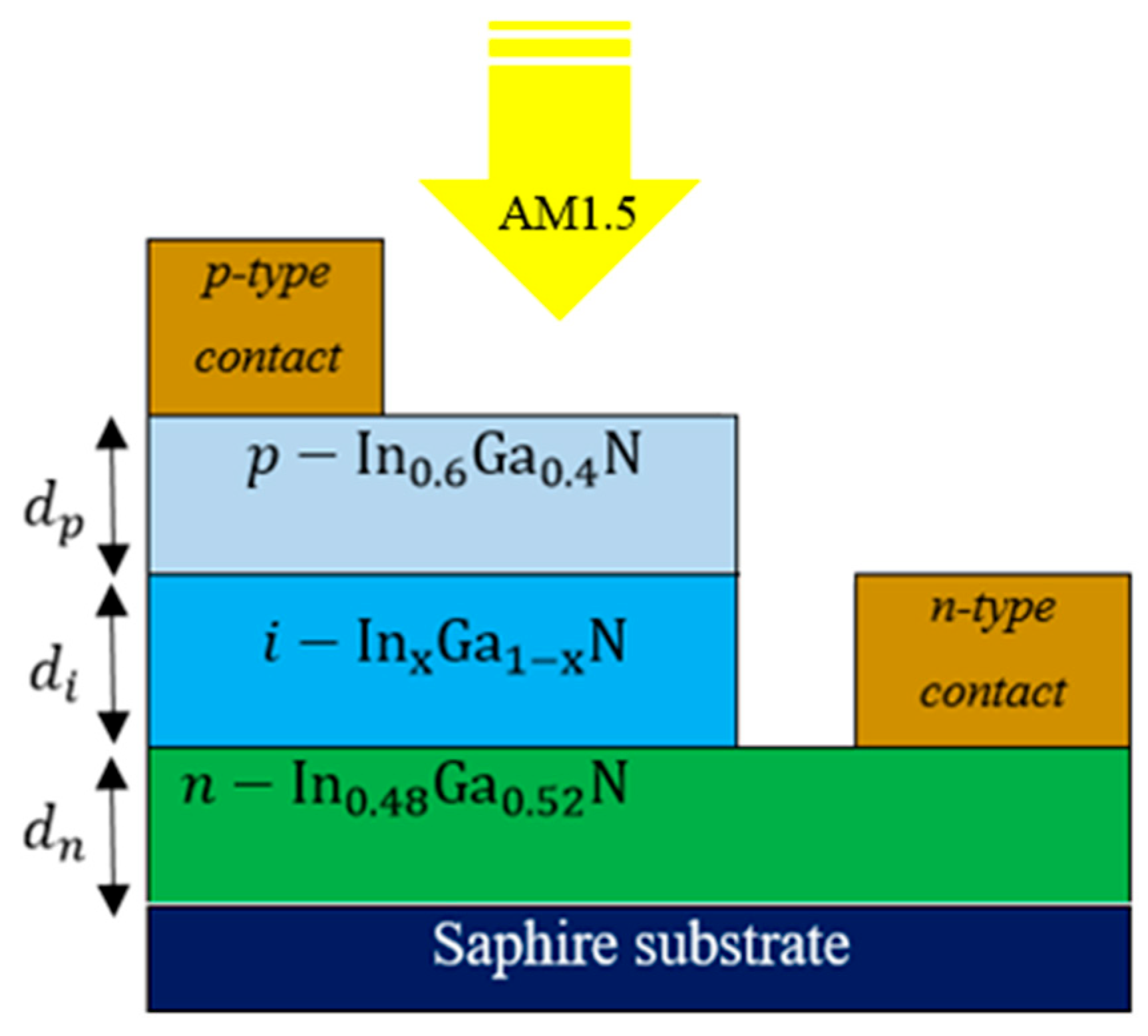
In this work, we focus on the p-i-n
-based solar cell structure, as illustrated in
Figure 1.
Figure 1 shows that the architecture, consisting of p-, i-, and n-type layers, is optimized to maximize light absorption and carrier separation. Our investigation evaluates the interplay between material properties, such as bandgap tuning, doping concentration, and layer thickness, and device architecture, with the goal of achieving higher energy conversion efficiency. SCAPS version 3.3.10 was utilized to simulate the proposed solar cell, a widely recognized tool for solar cell modeling and simulation. It plays a pivotal role in evaluating the feasibility of novel designs and optimizing physical parameters to maximize energy conversion efficiency. To enhance the readability of this work, we provide a list of the nomenclature and symbols used in this numerical simulation study, as outlined below in the nomenclature section.
The solar cell device under investigation consists of a p-i-n heterostructure grown on a sapphire substrate, with illumination incident from the p-contact side. It is composed of three primary layers: a p-type layer, which forms the base and also serves as the window layer; an i-type absorption layer for light harvesting; and a buried n-type emitter layer. This architecture is designed to establish an efficient built-in electric field for the separation and transport of photogenerated charge carriers.
Furthermore, while our model utilizes a conventional sapphire substrate to align with common industrial practice and the existing literature, we acknowledge that substrate engineering is a critical avenue for improving material quality. Alternative substrates such as ZnO, which offers a significantly better lattice match to InGaN, present a promising pathway to reducing dislocation densities and enhancing device performance, as has been previously demonstrated [
23]. Future experimental work should indeed consider such advanced substrate options in the practical realization of our optimized device design.
The initial indium compositions for the p-type and n-type layers were strategically selected to balance optoelectronic efficiency with material stability, guided by both theoretical principles and established experimental findings. The p-type composition was chosen to create favorable band offsets for efficient hole transport, while the n-type , with its lower indium content, offers superior crystal quality and higher electron mobility. This graded composition establishes a beneficial built-in electric field across the p-i-n structure, which promotes the separation of photogenerated charge carriers and enhances collection efficiency, forming the basis for our subsequent optimization studies.
The intrinsic (i-type) layer plays a critical role as the core of the device, designed to optimize charge carrier generation and separation. It ensures the full depletion of photogenerated carriers, which are then efficiently transported to their respective electrodes. This architecture creates a strong internal electric field, promoting efficient charge collection while minimizing recombination losses. As a result, the p-i-n structure is well-regarded for enhancing photocurrent generation and improving overall quantum efficiency [
24].
The SCAPS-1D platform enables precise modeling of solar cells by solving the coupled differential equations governing charge transport. Specifically, the Poisson equation describes the spatial distribution of the electrostatic potential (
) and establishes its relationship with the charge density:
where
e is the elementary charge,
is the vacuum permittivity,
is the relative permittivity,
p(x) and
n(x) are hole and electron densities,
and
represent donor and acceptor doping concentrations, and
and
are charge densities due to holes and electrons. This equation establishes the electric field profile within the device, which is critical for charge carrier separation and transport. Moreover, the continuity equations for electrons and holes describe their respective current densities as follows:
where
and
are current densities for electrons and holes,
G is the carrier generation rate, and R is the recombination rate. The generation rate depends on the material’s absorption coefficient and the incident photon flux, while the recombination rate is modeled using Shockley–Read–Hall (SRH) statistics. Hence, accurate modeling requires precise definition of the material parameters for
. Thus, the bandgap energy (
Eg) varies with the indium (In) composition (x) and is expressed as follows [
25]:
where
= 0.7 eV,
= 3.4 eV, and the bowing parameter C = 1.43 eV [
26] accounts for the deviation from linearity. It is important to note that the application of Equation (4) is subject to physical limitations inherent in the InGaN alloy system. The significant lattice mismatch (~11%) between the binary constituents, GaN and InN, induces substantial strain, particularly at high indium compositions. This can lead to thermodynamic instability and phase separation (i.e., the formation of In-rich and Ga-rich clusters), a phenomenon known as the “miscibility gap” [
27,
28]. In such cases of material inhomogeneity, the linear interpolation of the bandgap becomes less accurate, and the actual electronic properties can deviate from these idealized predictions. Therefore, our simulations are understood to be valid within the compositional ranges where InGaN can be grown as a stable, homogeneous alloy.
This tunable bandgap enables
to absorb a wide spectrum of solar radiation [
29,
30]. The relative permittivity (
) quantifies the material’s ability to reduce the electric field strength between charges and is given as follows [
31]:
The electron affinity (
) represents the energy required to move an electron from the conduction band to the vacuum level, calculated as follows [
32]:
The effective density of states for the conduction (
) and valence (
) bands are expressed as follows [
33]:
Carrier mobility (i.e.,
,
) quantifies the velocity of charge carriers under an electric field and depends on doping concentration
through the Caughey–Thomas model [
34,
35]:
Here,
,
and
are material-dependent parameters, and
is an empirical factor. These material properties, along with their spatial distribution, are crucial for accurately simulating charge transport and device performance. By integrating these equations and material parameters, SCAPS-1D provides a robust platform to investigate and optimize the performance of p-i-n
solar cells under standard AM1.5D illumination and at room temperature.
The power conversion efficiency of solar cells depends on key parameters, namely the open-circuit voltage
, the short-circuit current density
, and the fill factor FF, which are expressed as follows:
The reverse bias saturation current density
quantifies the leakage of minority carriers across the p-n junction. This leakage arises due to carrier recombination occurring in the neutral regions adjacent to the junction. It can be expressed as follows [
36]:
where
and
represent the diffusion lengths of minority carriers in the n and p regions, respectively.
and
denote the acceptor and donor concentrations, while
and
are the diffusion coefficients of minority carriers in the p and n regions.
It is important to note that the
and
constants for the ternary (In,Ga)N are derived using linear interpolation of the corresponding parameters for InN and GaN. The expressions for carrier diffusion lengths are as follows:
where
is the carrier lifetime obtained for InGaN as the linear interpolation of those of binary-related materials.
The carrier diffusion coefficients can be obtained as following:
The behavior of the FF is always affected by many factors, especially the series and shunt resistance, as well as partially the
values, as presented in the following equation [
37]:
where
.
The most important factor is the solar cell efficiency obtained as the ratio of the output power to the input power
, and it is expressed as follows [
25]:
where
is the optical input power of solar radiation AM1.5 G illumination
on the surface of solar cells.
To contribute to the improvement of solar energy conversion efficiency, this study considers the physical properties of the
alloy. The material-dependent parameters required for the modeling performed in this work are summarized in
Table 1. This table mainly illustrates the required parameters used in the numerical simulation of the investigated solar cell.
3. Results and Discussion
This section is devoted to discussing the results and findings obtained through the simulation. A significant challenge in solar energy research is the development of eco-friendly, cost-effective solar cells that maintain high efficiency (ɳ%) while utilizing ultra-thin absorber layers [
41]. Critical parameters, such as the acceptor and donor concentrations and the absorber layer thickness, play a pivotal role in determining the structural design and overall performance of solar cells. Optimizing these factors is essential for achieving superior energy conversion efficiency. In this study, simulations were performed at room temperature under standard solar conditions (1000 W/m
2, AM 1.5G) to simulate real-world operating conditions. Firstly, we applied the physical and structural parameters outlined in
Table 1 and
Table 2 to model the p-i-n solar cell consisting of p-type
, i-type
, and n-type
layers. The initial simulation results revealed an open-circuit voltage
of 0.89 V, a short-circuit current density
of 25.64 mA/cm
2, a fill factor FF of 83.68%, and an overall efficiency of conversion up to 18.10%.
Although ambient temperature (300 K) is commonly used as the reference condition for evaluating the performance of InGaN-based p-i-n solar cells, it is crucial to consider a broader temperature range for a more realistic assessment. In actual operating environments, these devices are subjected to significant thermal fluctuations, which can substantially influence their performance. This aspect has been previously investigated in our earlier work [
20,
42,
43]. Temperature variations can lead to bandgap narrowing, reduced open-circuit voltage, enhanced recombination processes, and diminished charge carrier mobility. Therefore, considering thermal effects is essential not only for evaluating the operational stability of the device but also for optimizing its design according to its intended application environment.
The optimizations were performed on the standard p-i-n solar cell structure by successively varying the thicknesses of the p-, i-, and n-layers to determine the optimal thickness for each. In addition, the uniform shallow donor density was varied between
and 1
to assess its impact on the solar cell’s efficiency. Similarly, the uniform shallow acceptor density was varied within the range of 1
to 8
to study its effect on performance. Finally, the indium content (x) in the
material of the intrinsic (i) layer was adjusted to examine its influence on the whole performance of the p-i-n solar cell. First, we optimized the thickness of the p-type layer (
) by varying it from 100 nm to 500 nm, as shown in
Figure 2.
Figure 2 illustrates the effect of varying the thickness of the p-type In
0.6Ga
0.4N layer on key performance parameters of the p-i-n InGaN-based solar cell. All other structural parameters were fixed: the intrinsic region remained In
0.52Ga
0.48N with an indium mole fraction x = 0.52 and a thickness d
i = 0.40 µm, while the n-type emitter was fixed at d
n = 0.06 µm. Panel (a) shows the relationship between the p-type layer thickness and two critical factors, efficiency (η) and fill factor (FF), while panel (b) displays the influence of p-type layer thickness on the short-circuit current density (
) and open-circuit voltage (
).
Figure 2a,b display the evolution of key performance parameters, efficiency, FF,
, and
, as functions of the p-layer thickness. It can be seen that increasing the p-layer thickness from 0.1 μm to 0.5 μm led to significant improvements in both photovoltaic conversion efficiency and
, which reached approximately 19.6% and 21.7% (28 mA/cm
2), respectively. The increase in efficiency is shown in
Figure 3a. Due to the enhanced light absorption and improved carrier collection efficiency associated with a thicker p-layer, greater charge carrier generation is promoted. However, it is important to note that the
increased slightly, by approximately 0.34%, with increasing dp , as shown in
Figure 3b. This small increase in
is likely due to the stronger internal electric field generated by the thicker p-layer, which enhances the separation of photogenerated electron–hole pairs, thus reducing recombination losses. In contrast, the FF showed a decrease, estimated to be 4.8%, as the p-layer thickness increased. This reduction in FF can be attributed to increased series resistance and potential charge transport losses in thicker layers, which slightly offset the gains in efficiency and current density. Despite this, the maximum values for efficiency,
, and
were obtained with a p-layer thickness of 0.5 μm, yielding values of 19.6%, 0.889 V, and 28 mA/cm
2, respectively. Thus, this demonstrates the critical role of optimizing the p-layer thickness in achieving the best trade-off between high efficiency, high current density, and acceptable fill factor. Moreover, the increase in efficiency and current density with thicker p-layers suggests that further improvements in carrier transport and light absorption are achievable by fine-tuning the thickness of each layer.
Figure 3a,b illustrate the impact of the i-layer (In
0.52Ga
0.48N) thickness (
) on the FF,
,
, and η of p-i-n InGaN-based solar cells. As shown, the thickness of the intrinsic i-layer plays a significant role in the performance of the solar cell. The design maintained rigorous structural parameter control: the intrinsic region remained In
0.52Ga
0.48N with an indium mole fraction x = 0.52 and p-type layer thickness d
p = 0.40 µm, and the n-type layer was fixed at d
n = 0.06 µm. The
was varied between 350 nm and 700 nm. In
Figure 4b, both the
and
exhibit moderate increases with increasing
. Specifically,
rises from 24.97 mA/cm
2 to 25.76 mA/cm
2, corresponding to a 3.16% increase as
increases from 350 nm to 700 nm. This increase is attributed to the enhanced photon absorption by the thicker i-layer, which generates a greater number of electron–hole pairs. Similarly,
increases from 0.883 to 0.907 V, a 2.7% increase, reflecting the improved charge carrier separation and reduced recombination. In addition,
Figure 4a reveals two distinct behaviors for η and FF as a function of
. A critical thickness (
) of approximately 0.4 μm is identified, which marks a shift in the efficiency behavior. For
, the efficiency decreases, while for
, it increases. Specifically, η slightly decreases from 17.9% to 17.87% when
is between 0.35 μm and 0.4 μm, representing a 0.17% reduction. However, for
0.4 μm, η increases significantly by 2.7%, reaching a maximum value of 18.35% at
. In contrast,
Figure 4b shows that the FF decreases gradually from 81.3% to 78.35% as
increases from 0.35 μm to 0.6 μm, a drop of 3.76%. Beyond 0.6 μm, there is a slight increase in the FF, which reaches 78.5% at
. These results are consistent with the understanding that increasing the thickness of the absorber layer enhances its capacity to absorb light. As the i-layer becomes thicker, it absorbs more photons, leading to the generation of more electron–hole pairs. This also reduces the recombination at the interface and increases the width of the depletion region, which contributes to higher charge carrier separation and collection efficiency, which is in good agreement with previously published works [
44].
Figure 4 presents a comprehensive parametric analysis examining the influence of n-layer thickness (d
n) variation across a range of 0.01–0.10 μm on critical photovoltaic performance parameters within p-i-n InGaN-based solar cell configurations. The experimental framework maintained rigorous structural parameter control: indium content was fixed at x = 0.52 (
composition), intrinsic layer thickness was held constant at d
i = 0.4 μm, and p-type layer thickness remained at d
p = 0.01 μm, thereby isolating the specific contribution of n-layer thickness modulation to overall device performance characteristics.
Figure 4a shows how η and FF change with the n-layer thickness (
). Both parameters follow similar trends as
increases from 10 nm to 100 nm. Specifically, η decreases slightly from 17.91% to 17.735%, a reduction of about 1%. This minor decrease is attributed to the increase in series resistance and potential charge transport losses in the thicker n-layer, which slightly diminishes the overall efficiency. While a thicker n-layer can provide more surface area for charge collection, it also leads to longer paths for carrier transport, increasing recombination rates and reducing the overall efficiency of the device.
In contrast,
Figure 4b illustrates the opposite trend for
and
. Both parameters show a slight increase as
increases, with the
rising by approximately 0.38% and the
increasing by about 0.4%. These increases suggest that a thicker n-layer facilitates better charge carrier transport, leading to improved charge separation and reduced recombination losses at the interface between the n-layer and the intrinsic layer. The small but noticeable improvements in
and
are indicative of a stronger internal electric field and better alignment of the energy bands, both of which enhance the overall device performance. Moreover, while the increase in
and
is modest, it is still significant, demonstrating that the n-layer thickness plays a critical role in optimizing the transport properties of the solar cell. A thicker n-layer can enhance the electric field, which contributes to better carrier collection and less recombination, improving the overall charge extraction from the device. However, this improvement comes with a trade-off, as the decrease in η suggests that increasing
beyond an optimal value could result in diminishing returns. The thicker n-layer leads to higher resistive losses and could limit the photocurrent generation due to additional material absorption or carrier scattering. Therefore, careful optimization of the n-layer thickness is essential to balance these competing effects and achieve the best overall performance for the solar cell.
To evaluate the effect of doping concentration, we simulated the structure with p-layer doping concentrations (
) ranging from
and n-layer doping concentrations (
) ranging from
, each considered separately. The layer thicknesses were set to 20 nm, 0.4 μm, and 0.2 μm for the n-, i-, and p-layers, respectively, and the indium content in the i-layer was fixed at x = 0.52 (
composition), while all other parameters were maintained as specified in
Table 1. The results for p-layer and n-layer doping concentrations are shown in
Figure 5 and
Figure 6, respectively. We commenced by investigating the variation in the doping concentration of the p-layer (
) on the key output parameters of the solar cell, including FF and η, shown in
Figure 6a, and
and
, presented in
Figure 6b. As shown in panel 6a and panel 6b, all key parameters, except for
, exhibit a near-exponential increase, reaching a saturation point at an
concentration of roughly
. Specifically, a maximum efficiency of around 19.2% is achieved at
, representing an 8.47% increase across the concentration range. Similarly, the FF increases by approximately 8.6%, and
improves by about 25.27% within the same doping concentration range. This enhancement in efficiency and
is attributed to the improved management of carrier dynamics, particularly the reduction in recombination losses, which allows for a more effective separation of the electron–hole pairs. The increase in
reflects the optimization of internal processes, such as the enhanced alignment of quasi-Fermi levels and reduced recombination at the p-n junction. However, the increase in
leads to a noticeable decrease in
, which exhibits an almost exponential decline from 25.25 to 22.2 mA/cm
2, representing a 13.74% reduction. This decrease can be explained by the reduction in radiative recombination, which, although beneficial for improving
, limits the net generation of carriers and, consequently, reduces the short-circuit current density. This trade-off underscores the delicate balance between improving voltage and maintaining a high current density in the optimization of solar cell performance.
As illustrated in
Figure 6a,b, all major parameters, except for
, show a nearly exponential increase before reaching saturation at a donor doping concentration of approximately
. Additionally, in
Figure 7a, both the efficiency (η) and FF exhibit similar trends, increasing as
rises. The efficiency reaches a maximum of 17.98%, corresponding to a 5.76% increase, while the fill factor achieves a peak value of 80.6%, representing a 7.47% improvement. These improvements indicate that increasing the donor concentration optimizes the charge transport properties of the window layer, which enhances overall carrier collection and reduces recombination losses, thereby improving both η and FF. Conversely,
Figure 7b shows the behavior of
and
. The
increases slightly, from 25.165 to 25.2085 mA/cm
2, reflecting a 0.17% increase as
increases from
to
. This modest increase in
is consistent with the enhanced carrier transport and the increased photon absorption in the device due to the optimized donor concentration. In contrast, the
decreases exponentially, dropping from 0.8990 to 0.8858 V, which corresponds to a 1.49% reduction across the same doping range. This reduction in
can be explained by the higher concentration of donor impurities, which leads to increased recombination at the junction and a reduction in the built-in electric field, thus lowering the voltage.
These results demonstrate the delicate balance between optimizing and through doping concentration. While increasing improves current density and efficiency, it also introduces trade-offs, such as the slight reduction in . Therefore, tuning the donor concentration is crucial to maximizing the overall performance of the solar cell, where the goal is to achieve the best combination of high photocurrent and voltage.
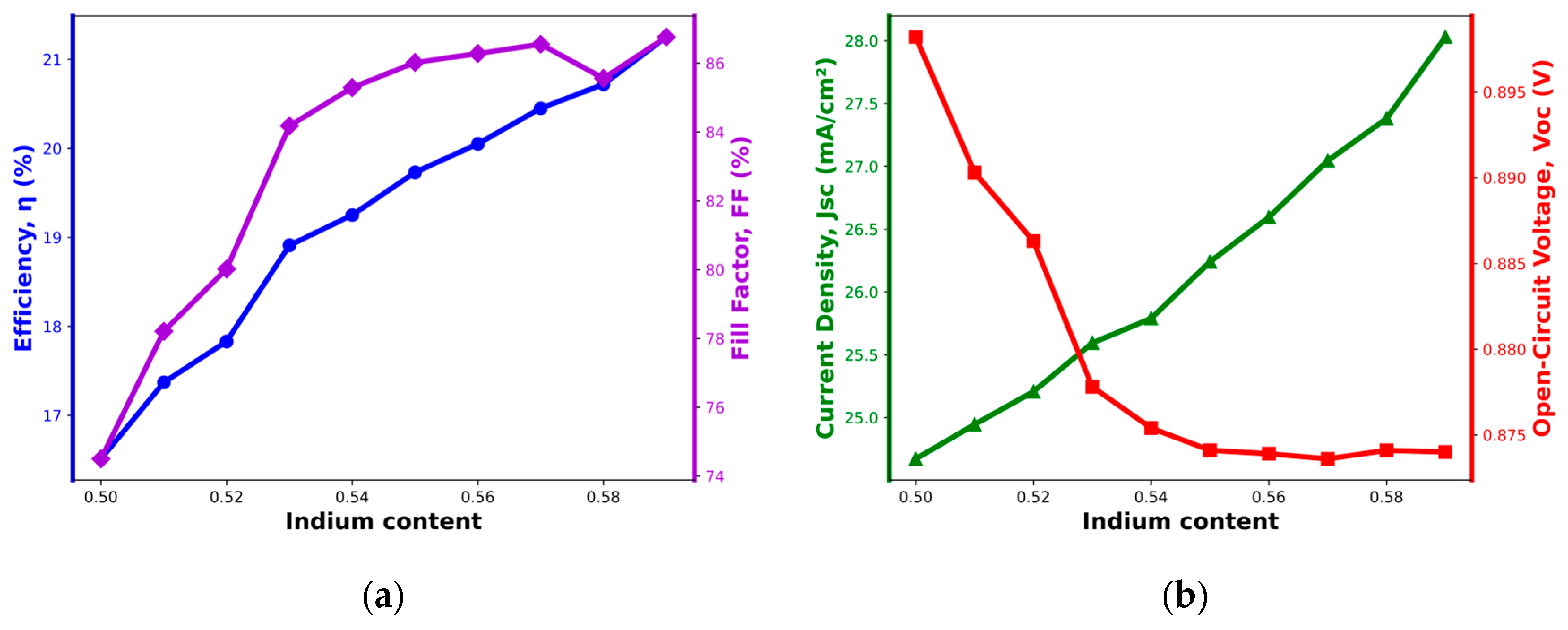
Here, the optimization of the indium composition (x) in the active layer (
) has been investigated by adjusting the energy bandgap between 1.69 eV and 1.46 eV.
Figure 7 presents the variations in key solar cell parameters efficiency, FF,
, as well as
as functions of the indium composition, which goes from 0.50 to 0.59, which has been selected to provide reliable and significant simulation results. The design employed rigorous parametric control: intrinsic layer thickness was maintained constant at d
i = 0.4 μm, p-type layer thickness remained fixed at d
p = 0.2 μm, and n-type layer thickness was held at d
n = 0.06 μm, thereby isolating the specific contribution of indium content modulation to overall device performance metrics.
From
Figure 7a, it is evident that η increases linearly, rising from 16.46% to over 21.40%, corresponding to a substantial 30.01% improvement within the studied range of indium content. This enhancement can be attributed to the reduction in bandgap energy as the indium concentration increases, which leads to greater photon absorption, especially in the low-energy photon range. As a result, the intrinsic i-layer absorbs more light, which increases the generation of electron–hole pairs and subsequently boosts the
, significantly improving the total output of the solar cell. Furthermore, the FF increases by approximately 16.1%, reaching a maximum value of 86.4%, indicating improved charge collection and reduced recombination.
Moreover,
Figure 7b shows the behavior of
and
as a function of indium content. Two distinct trends can be observed. First, the
increases from 24.2 to 28.2 mA/cm
2, a 16.52% improvement. This increase is primarily due to enhanced photon absorption and the subsequent generation of more electron–hole pairs. As the indium concentration increases, the narrowing of the bandgap allows for more effective absorption of photons, particularly in the visible and near-infrared regions, which contributes to the observed rise in
. In contrast, the
exhibits a quasi-exponential decrease, dropping from 0.898 to 0.874 V, representing a 2.75% reduction. A critical threshold,
, is identified, which governs the behavior of
: for indium fractions lower than
, the
continues to decrease, while for fractions higher than
, the
stabilizes at approximately 0.874 V. This behavior can be explained by the interplay between the built-in potential of the junction and the material’s properties. At
, a maximum
of around 0.9 V is observed. As
increases, the polarization-induced potential barrier initially contributes to a higher
, due to better band alignment between the p-type and n-type layers. However, beyond a certain indium content, material strain and defect formation increase, which leads to enhanced carrier recombination. This recombination reduces the effective charge separation at the junction, thereby lowering the
. Therefore, while increasing the indium content improves
and efficiency due to enhanced photon absorption, it also leads to a decrease in
due to the increased strain and recombination at higher indium concentrations. The observed trade-off between
and
emphasizes the importance of optimizing the indium composition to balance these effects and achieve the best overall performance for the solar cell. Despite that, this study emphasizes the importance of optimizing layer thicknesses, doping concentrations, and indium composition in enhancing the performance of
-based p-i-n solar cells. Future work should focus on experimental validation of these findings, strain management strategies for high indium content, and the development of tandem architectures to further boost efficiency. Additionally, addressing interface properties and evaluating environmental stability will be crucial for advancing these devices toward practical and durable applications in renewable energy systems.
While this study focuses on optimizing a specific compositional framework, it is worth noting that the pursuit of wider bandgap tunability in InGaN systems is an active area of research. Pushing indium concentrations to their limits presents significant thermodynamic and crystallographic challenges. Consequently, alternative materials engineering philosophies are gaining traction. These include the use of quantum-confined heterostructures (e.g., quantum wells) to manage strain, the development of novel compliant substrates, and the exploration of quaternary alloys like BInGaN, which may offer comparable bandgap modulation with improved material stability [
45]. Such advanced methodologies represent a viable pathway toward realizing the full potential of nitride-based photovoltaics. Finally, while the present simulations were conducted at a standard temperature of 300 K, we acknowledge that the thermal stability of these devices is of paramount practical interest. As we have demonstrated in previous work [
37], temperature fluctuations significantly impact device performance through mechanisms like bandgap narrowing and increased recombination rates. Future investigations should therefore consider the optimization of these device structures across a wider range of operating temperatures to ensure robust performance in real-world terrestrial and aerospace environments.


 ,
, 


