Article

Nanoindentation-Induced Deformation Mechanisms in Sintered Silver: A Multiscale Study Combining Experimental and Molecular Dynamics Simulations

1
College of Intelligent Robotics and Advanced Manufacturing, Fudan University, Shanghai 200433, China
2
Research Institute of Fudan University in Ningbo, Ningbo 315336, China
*
Author to whom correspondence should be addressed.
Crystals 2025, 15(7), 620; https://doi.org/10.3390/cryst15070620
Submission received: 21 May 2025 / Revised: 24 June 2025 / Accepted: 30 June 2025 / Published: 2 July 2025
(This article belongs to the Section Crystal Engineering)

Abstract

Sintered silver, widely used in WBG electronic device packaging for its excellent electrothermal properties and high-temperature stability, faces challenges in macroscopic mechanical behavior and reliability due to porosity, especially for pressureless sintered silver. However, the intrinsic pores inside sintered material introduce uncertainties during nanoindentation tests for mechanical characterization. This study investigated the impact of pore distribution on the dislocation behavior of pressureless sintered silver during nanoindentation. Firstly, pressureless sintered silver models with 8–33% porosity were prepared and characterized through scanning electron microscope (SEM) for porosity, electron backscatter diffraction (EBSD) for the geometrically necessary dislocation (GND) density distribution, and transmission electron microscopy (TEM) for the crystal structure and microscopic strain. The EBSD results indicated that nanoindentation caused localized plastic deformation in sintered silver, closely related to its porous structure. The TEM results revealed that sintered silver undergoes dislocation slip during nanoindentation, leading to complex dislocation network formation, while the strain decreased with distance from the indentation. To further investigate the relationship of pore distribution and dislocation behavior during nanoindentation, molecular dynamics (MD) simulations were carried out. The MD results revealed that the dislocation distribution was consistent with the EBSD and TEM results. During loading, with the increased porosity from 10% to 23.7%, the total dislocation length was reduced by 63%, while it led to a 38% increase in total dislocation length with the average pore size decreased from 3.84 nm to 2.88 nm under similar porosity conditions. This study improves the understanding of the deformation mechanisms of porous sintered silver under nanoindentation and provides insight into the mechanical characterization of porous materials.

1. Introduction

With the development of power electronics, wide band-gap (WBG) electronic components have been widely used [1,2,3]. Silver sintering technology, due to its excellent properties and reliability, has become crucial for interconnecting high-temperature, high-power WBG devices [4,5,6,7]. The porosity of sintered silver greatly affects its mechanical properties, potentially causing cracks and compromising reliability [8,9]. Researchers have been focused on optimizing the mechanical properties through materials, processing conditions, and interconnect designs [10,11,12,13,14,15,16,17]. During the actual applications, the thickness of such interconnect materials is usually around 20 μm to 100 μm. For characterizing the mechanical properties, nanoindentation technology is usually applied [18,19]. To gain a deeper understanding of the microstructure of sintered silver and its effect on mechanical properties, advanced characterization techniques such as electron backscatter diffraction [20,21,22] and transmission electron microscopy [23,24,25] have been widely used. Recent studies have focused on the relationship between the microstructure and mechanical properties of sintered silver particles. Xu et al. [26] developed a reverse analysis method to extract constitutive parameters of silver nanoparticles (AgNPs) from nanoindentation experiments, proving effective for predicting stress–strain relationships.
Due to the intrinsic porous structure, the nanoindentation results for sintered silver fluctuate, mainly due to the porous microstructures and the grain boundaries. During nanoindentation tests, the indenter may cause a stress concentration point and a crack source during deformation. Wang et al. [27] found through finite element simulation and experimental verification that the pores of AlN ceramic at grain boundaries are prone to expand and connect under applied load, which ultimately leads to cracking of the material along the grain boundaries. Yang et al. [28] observed the amorphization of KDP crystals after nanoindentation by TEM, and combined MD simulations to reveal the mechanism of deformation behaviors such as amorphization and dislocations. These studies showed that the combination of experimental and MD simulations provided an effective method for further analysis of material properties during nanoindentation measurements.
However, the mechanism of the effect of pore structure on the nanoindentation measurements is still unclear. Further investigation into the defect evolution and elastoplastic deformation of sintered silver is needed. Therefore, this study presents an analysis of pressureless sintered silver subjected to nanoindentation experiments. The scanning electron microscope (SEM) results confirmed the samples’ microstructural characteristics, establishing a reliable basis for subsequent electron backscatter diffraction (EBSD) and transmission electron microscopy (TEM) analyses. By integrating characterization techniques (SEM, EBSD, and TEM) with molecular dynamics (MD) simulations, the study delves into how pore distribution influences the deformation mechanisms of pressureless sintered silver during nanoindentation. It elucidates the interaction between pore structure and dislocation dynamics, offering a theoretical foundation for enhancing the practical performance of sintered silver.

2. Materials and Methods

2.1. Materials

The sintered silver samples investigated in this study consisted of 85 wt% sub-micron silver particles and 15 wt% organic solvents. The solvent for silver paste was formulated with terpineol (T), which served as a dispersant and polyethylene glycol (PEG), which functioned as a binder, in a mass ratio of 1:2.
The sintered silver joint sample preparation followed a three-step process: dispensing, die attachment, and pressureless sintering. First, the silver paste was precisely dispensed onto a direct bonded copper (DBC) substrate in a cross-pattern using an automated dispensing system with controlled pressure and speed. Next, silver-plated silicon dummy chips (4 × 4 × 0.32 mm3) were accurately positioned and attached onto the paste pattern using an automatic die bonder with precisely controlled attachment pressure. Finally, the assembled samples underwent pressureless sintering in a nitrogen atmosphere following a designed thermal profile: heating at 5 °C/min to 130 °C with a 30 min hold, further heating to 260 °C with a 2 h hold, and then cooling to room temperature at 5 °C/min. This sintering process effectively removed the organic components while promoting the formation of sintering necks between silver particles, resulting in a porous yet mechanically robust silver joint structure.
To characterize the microstructure of the sintered silver interconnection layer, cross-sectional samples of the sintered silver joints were prepared. The 6 parallel sintered silver joint samples were cut and mounted in a single epoxy resin, followed by vacuum treatment for 30 min. The samples were then left to cure at room temperature for 12 h. Systematic grinding was performed using a LaboForce-100 semi-automatic grinder manufactured by Struers, based in Copenhagen, Denmark. Initially, coarse grinding was carried out with 120-grit sandpaper, progressing systematically to finer grits up to 3000-grit. Subsequently, fine polishing was conducted using first 1 μm and then 0.25 μm polishing suspensions. After thorough ultrasonic cleaning and drying, the sample surface quality was confirmed using an optical microscope, thereby completing the sample preparation process.

2.2. Experimental Methods

In this paper, the nanoindentation instrument iNano produced by KLA, San Jose, CA, USA, is used. The results of nanoindentation were analyzed theoretically based on the Oliver–Pharr method to obtain the hardness and elastic modulus.
Morphology and porosity analysis were performed on samples with polished surfaces using a Gemini 300 field emission scanning electron microscope (SEM) from ZEISS, Oberkochen, Germany. The porosity was then calculated by processing the SEM images with image analysis software ImageJ 1.53. The porosity is calculated as follows:
ω = ω p o r e ω t o t a l ,
where ω p o r e represents the pore area and ω t o t a l represents the total chip bonding area.
Electron backscatter diffraction (EBSD) analysis was performed on an Oxford C-Swift+ system equipped with a field emission scanning electron microscope. To obtain high-quality EBSD images, the sample surfaces were first subjected to chemical–mechanical polishing (CMP) to remove the surface strain layer. The EBSD scans were then performed at the cross-section of the nanoindentation region, with the accelerating voltage at 20 kV and the working distance at 12.1 mm. Finally, the EBSD data were analyzed using AZtecCrystal 2.1 software to evaluate grain orientation distribution and local strain distribution, as well as to calculate the geometrically necessary dislocation (GND) density. GND refers to dislocations generated due to geometric constraints during the plastic deformation process of materials, serving as an important indicator of local deformation during nanoindentation [29,30,31]. The AZtecCrystal 2.1 software employs a kernel average misorientation (KAM) method to quantify local strain gradients, where the orientation difference between neighboring measurement points is used to calculate the GND density according to the following equation [32,33]:
ρ G N D = θ μ b
where μ is the magnitude of the Burgers vector, b is the characteristic length of the dislocation, and ∇θ is the orientation gradient. It is worth mentioning that data points with confidence index (CI) below 0.1 were excluded from the analysis to maintain data quality [34].
Transmission electron microscopy (TEM) samples were prepared using a dual-beam focused ion beam microscope (FEI Scios 2). To protect the surface of the samples, a protective layer of platinum (Pt) approximately 2 μm thick was deposited on the indentation region before extraction. Subsequently, cross-sectioned thin slices were cut using a Ga+ ion beam with an accelerating voltage of 30 kV. The slice needed to be precisely positioned at the deepest part of the indentation, with a depth of about 5 μm. TEM observations were performed on a FEI Tecnai F20 field emission transmission electron microscope manufactured by Thermo Fisher Scientific, located in Hillsboro, OR, USA, and operated at 200 kV. Bright-field (BF) and dark-field (DF) imaging modes were used to observe dislocation structure and distribution. Selected area electron diffraction (SAED) was applied afterwards to determine the crystal orientation and analyze the strain field. To study the deformation, the microstructure of different regions around the indentation was characterized, including the regions directly below, at the edges, and far away from the indentation test point.
The samples used in this study were derived from 2 of the 6 parallel samples. Both samples underwent initial nanoindentation experiments and SEM characterization. SEM results indicated that the two samples possessed comparable microstructural characteristics. After SEM, the samples were subjected to subsequent EBSD and TEM analyses for the characterization of microstructure morphology and deformation behaviors.

2.3. Simulation Methods

To investigate the dislocation behavior during nanoindentation at an atomic scale, molecular dynamics (MD) simulations were conducted in this study. Considering the size of the nanoindenter test region and the limitation of MD modeling, this study only focused on monocrystalline silver (0 0 1) with various pore distributions. The modeling details and simulation processes are shown in Figure 1.
Firstly, the nanoindentation MD models of monocrystalline silver (0 0 1) were developed. To simplify the simulation process, pores were modeled as ideal spherical structures within a cubic lattice. The cubic structure and spherical pores were assumed to extend infinitely with a periodic arrangement. Under this idealized model, the porosity was calculated as the ratio of the spherical pore volume to the volume of the cubic unit cell. This approach assumes uniform pore distribution and consistent spacing, allowing for straightforward porosity calculations while maintaining computational efficiency. Based on this method, several distinct sets of pore characteristics were generated, as illustrated in Figure 1.
The model consists of an indenter and a silver specimen. As shown in Figure 1, a spherical diamond indenter (purple, 10 nm diameter) was used for nanoindentation simulation. The atoms in the silver specimens were divided into three distinct layers according to their boundary conditions and physical properties: (1) boundary fixed layer atoms (red, 2 nm thickness at the bottom), where atomic positions remain fixed throughout the simulation; (2) constant temperature layer atoms (blue, 2 nm thickness), which maintain thermal equilibrium by coupling with a heat bath; and (3) Newtonian layer atoms (yellow, 20 nm thickness), which follow classical molecular dynamics equations of motion and represent the primary deformation zone. During the nanoindentation test, the specimen is generally required to be fixed on the platform. Therefore, it is necessary to set a fixed layer of atoms at the bottom of the silver model. The fixed layer atom has a fixed effect on the specimen so that the specimen does not move in the Z-axis direction. The atom connected to the fixed layer atom was defined as the constant temperature layer atom, which was set to a constant temperature state by a velocity determination method. The purpose is to absorb the heat generated by the indenter or silicon carbide specimen during the indentation process. Among them, the motion of atoms in the constant temperature layer and Newtonian layer in the system follows Newton’s second law. To tune the simulation results closer to the experiments, the Z-axis of the indentation model was set as the free boundary condition. To eliminate the influence of the specimen boundary on the simulation results, the specimen was set to periodic boundary conditions in both the X and Y directions.
After constructing the model, the atoms were initially arranged on a lattice, followed by energy minimization and relaxation for stabilization. Relaxation was performed using an isothermal isobaric (NPT) ensemble until the system energy stabilized and reached a minimum. The nanoindentation simulation was carried out based on such a stabilized MD model. The MD simulation process of nanoindentation was set as follows: Firstly, the diamond indenter was set to descend at a constant velocity during loading, and then ascend at the same constant velocity during unloading once the maximum indentation depth was reached. In this process, the ambient temperature is set to 298 K, interatomic interactions between silver atoms are governed by the EAM potential [35], while the interaction between the indenter and silver atoms of the Newtonian layer is expressed using the Morse potential with parameters D = 0.1 eV, α = 1.7 Ǻ−1, and r0 = 2.2 Ǻ [36]. The diamond indenter is treated as a rigid body due to its high hardness compared to silver [37]. The indentation parameters were set to a maximum penetration depth of 30 Å, an initial distance of 10 Å from the indenter to the surface, and a loading speed of 0.1 Å/ps. To ensure statistical reliability and quantify the uncertainty in simulation results, each group (Groups 0–3) was subjected to five independent simulation runs with the same identical structural and simulation parameters.
Finally, the MD simulation results obtained by LAMMPS 3Nov2022 software were imported into OVITO 3.7.11 and Origin 2025b software to complete the drawing of load–depth curves. Dislocation distribution maps of the monocrystalline silver during the indentation of the diamond indenter were obtained by using the Dislocation Extraction Algorithm (DXA). Furthermore, statistical analysis was performed on five repeated simulations for each group to calculate the mean and standard deviation of total dislocation length at both the loading completion stage and unloading completion stage, thereby ensuring the reliability of the simulation results.

3. Results and Discussion

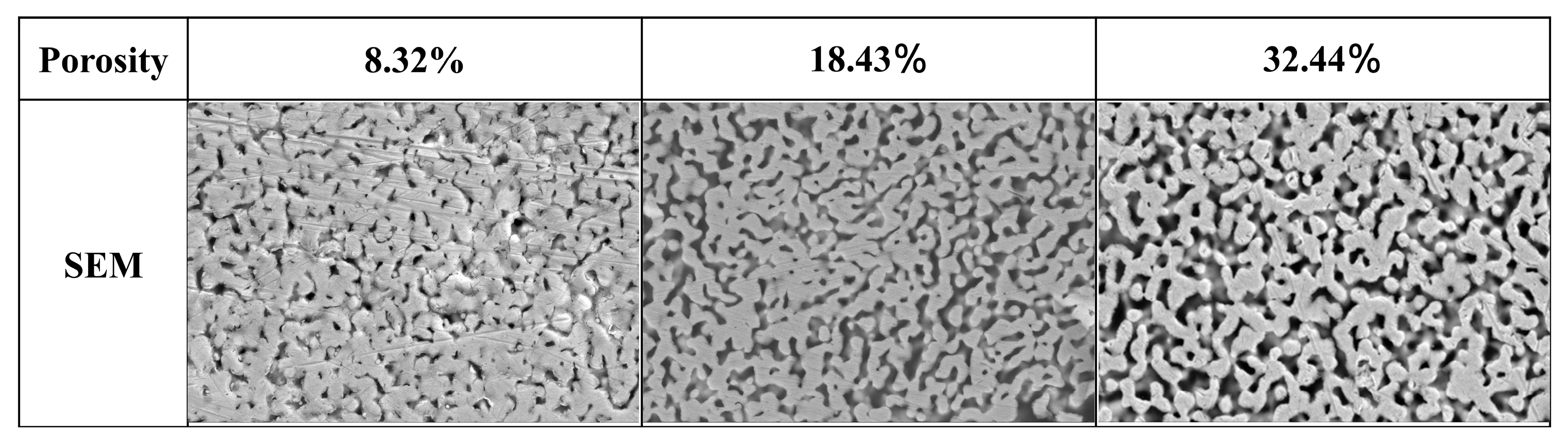
3.1. SEM Characterization Results

3.1.1. Porosity Characterization

This study employed two parallel sintered silver samples for SEM characterization. For each sample, 10 random locations were selected for SEM imaging, totaling 20 observation areas. Subsequently, the acquired SEM images were processed using ImageJ 1.53 software to calculate the porosity of each region.
Figure 2 presents the SEM images and porosity for three different positions of the sintered silver sample. Results indicate that the porosity of the sintered silver sample varies between approximately 8% and 33%, reflecting the spatial inhomogeneity of the microstructure of sintered silver. In addition, the two parallel samples have comparable microstructural characteristics. This demonstrates the consistency and repeatability of the sample preparation process. Three representative regions were selected and displayed in Figure 2 to visually demonstrate the porous structure characteristics. The SEM characterization highlighted the diverse porosity of sintered silver, providing experimental data for subsequent MD simulations.

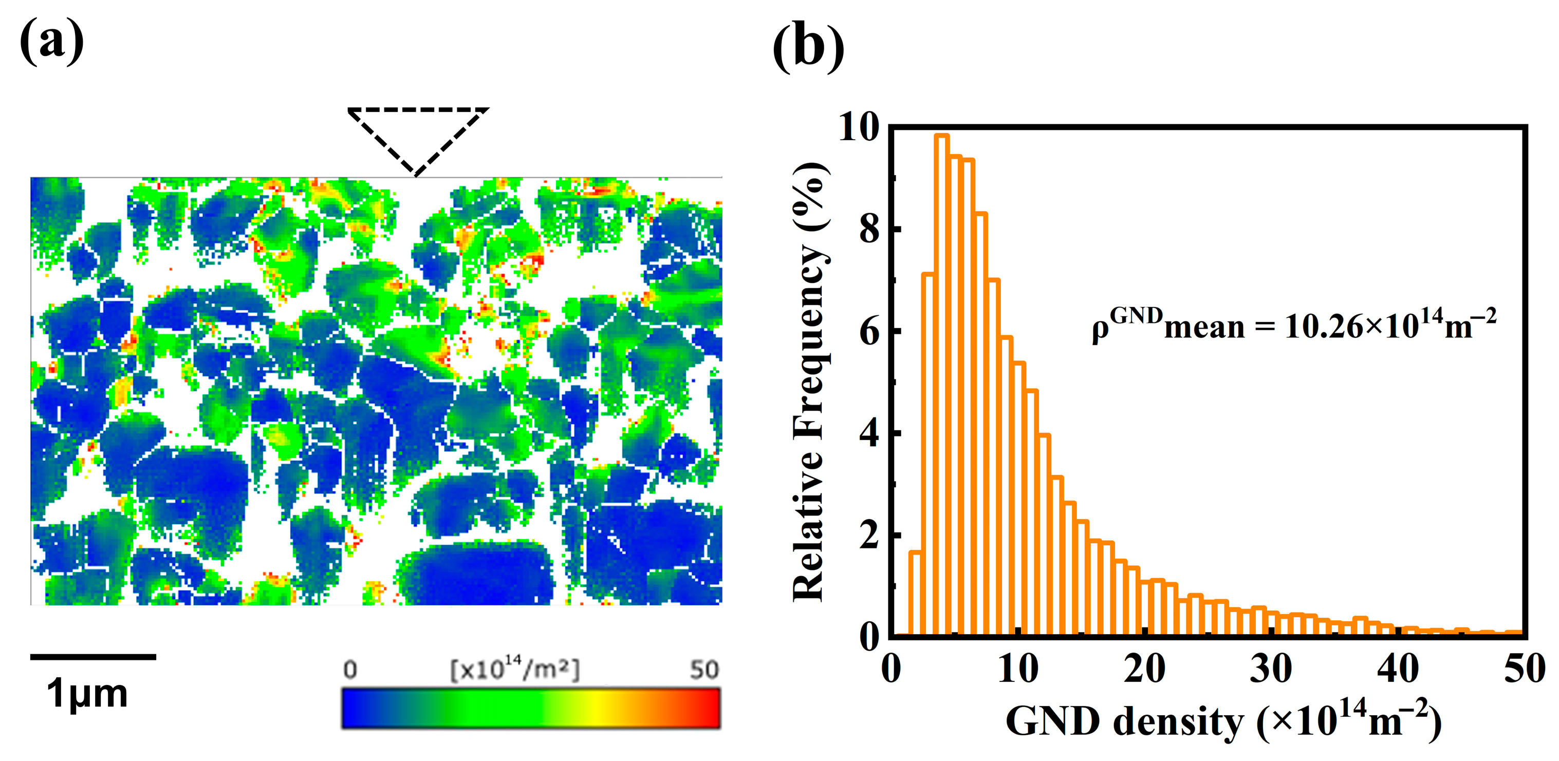
3.1.2. EBSD Characterization Results

EBSD characterization reveals that nanoindentation induces an “island-like” GND density distribution in sintered silver, which was influenced by the porous structure. Figure 3 presents the EBSD analysis of the nanoindentation area in the sintered silver sample. The analysis was conducted on a cross-sectional plane aligned with the nanoindentation direction. Figure 3a displays the GND density distribution, where triangular markers indicate the indentation position. Colors represent GND density levels, with blue denoting low density to red indicating high density. Figure 3b provides a statistical histogram of the GND density.
As shown in Figure 3a, the EBSD results reveal an inhomogeneous GND density distribution around the indentation. The GND density is higher near the indentation, reflecting greater plastic deformation. With the increase in distance from the indentation, the GND density decreased, which indicates an indentation-induced strain gradient. It is worth noting that the GND density is higher in the vicinity of pores. These pores could serve as stress concentration regions, leading to dislocation formation and pile-up. This confirms that stress concentration at pore edges enhances local plastic deformation.
Furthermore, the GND density distribution exhibits discontinuities associated with the porous network structure. Pores restrict dislocation movement, leading to their accumulation between adjacent pores and the formation of “island-like” regions with high GND density. The statistical distribution of the GND density is shown in Figure 3b. The average GND density is 10.26 × 10¹⁴ m−2, with most areas falling within the range of 5–15 × 1014 m−2. Regions with GND densities exceeding 20 × 1014 m−2 are less common, indicating that plastic deformation is primarily localized near the indentation test point.
Additionally, intergranular variations in GND density distribution exist within the indentation’s influence zone, likely due to differing deformation capacities of grains with varying orientations. The GND density distribution also reflects the non-uniform accumulation of dislocations in the microstructure. Especially in porous sintered silver, the pores not only act as stress concentration sources to promote dislocation formation, but also act as barriers to dislocation movement, leading to dislocation accumulation as shown in the GND distribution.

3.2. TEM Characterization Results

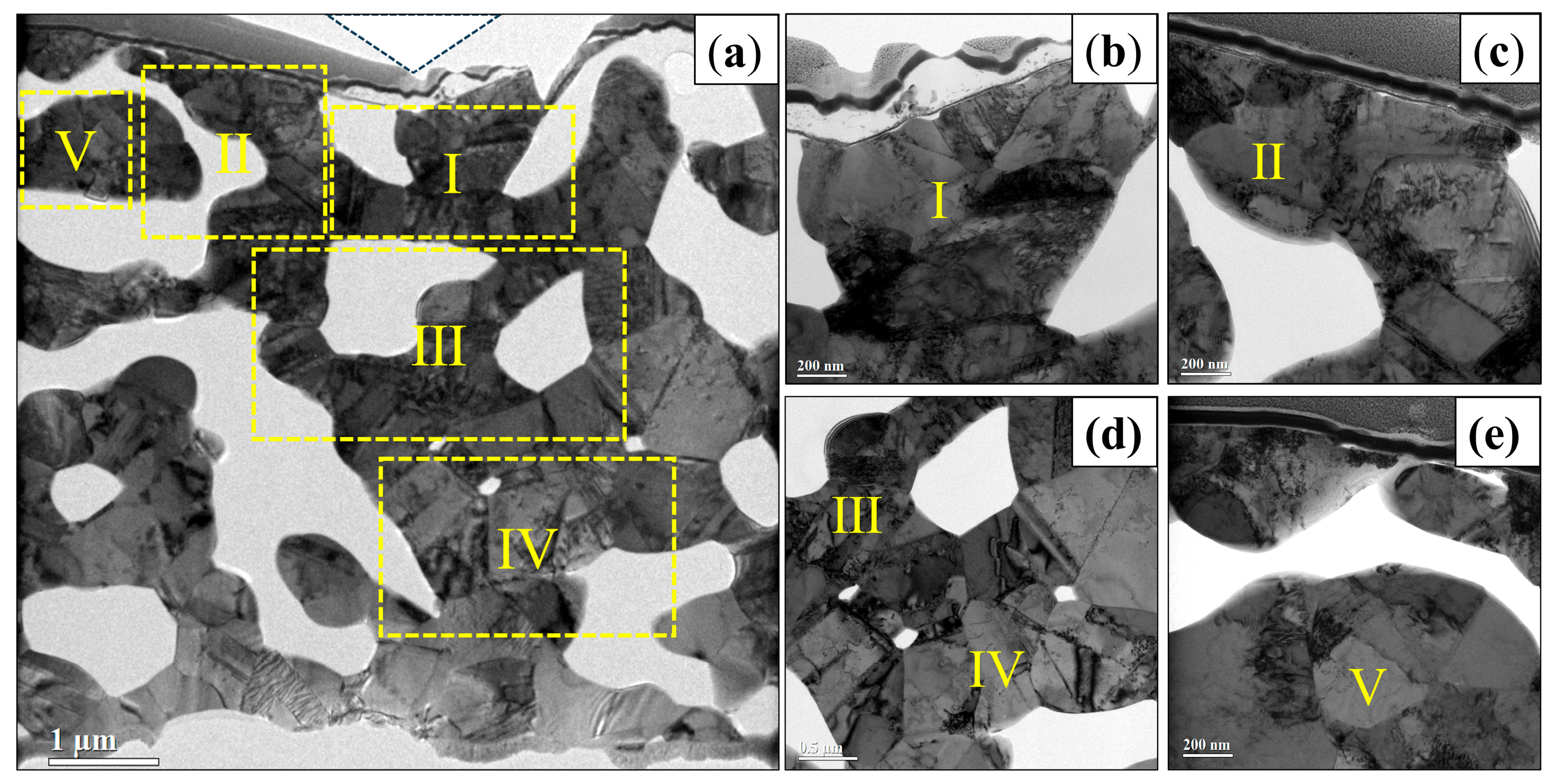
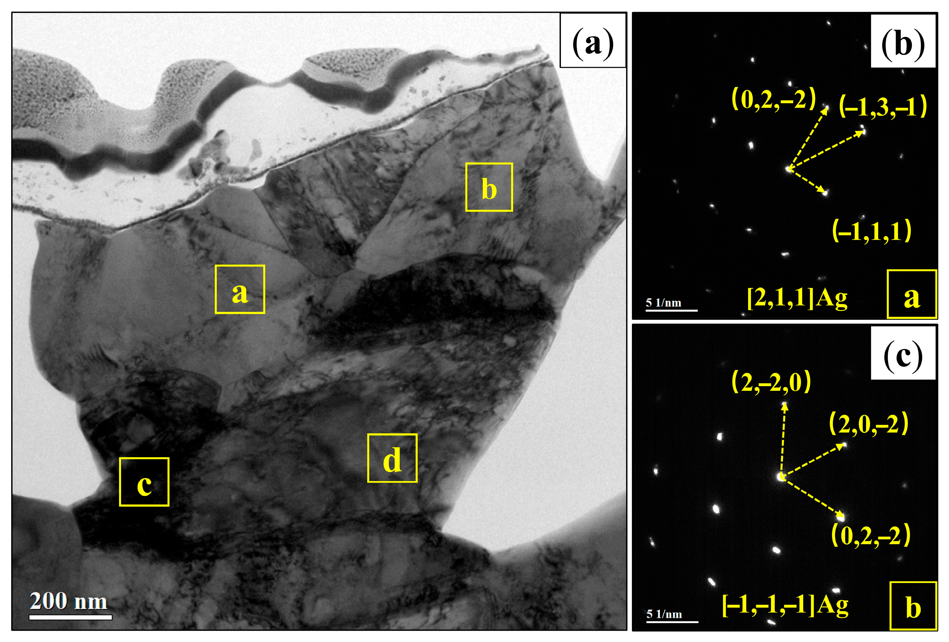
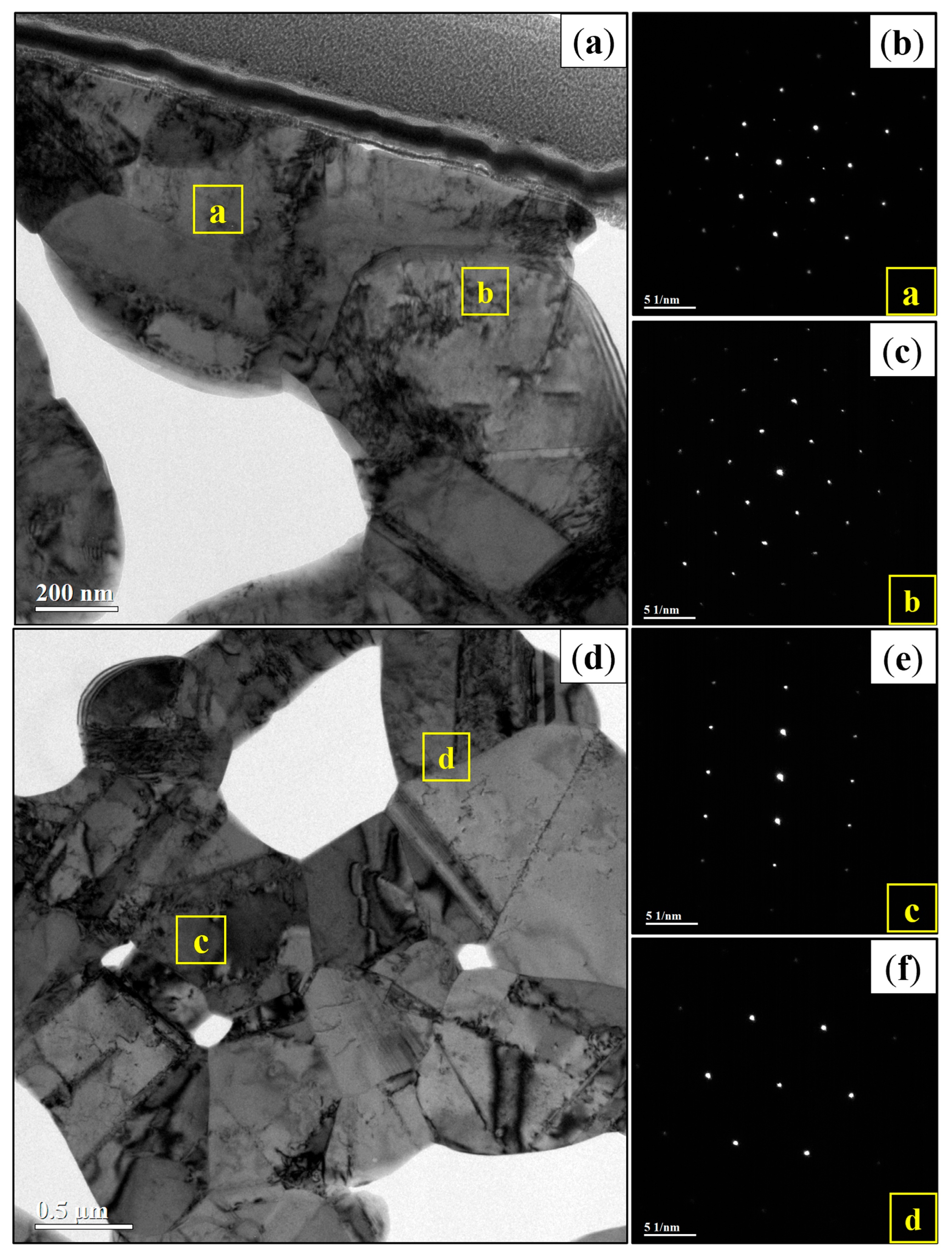
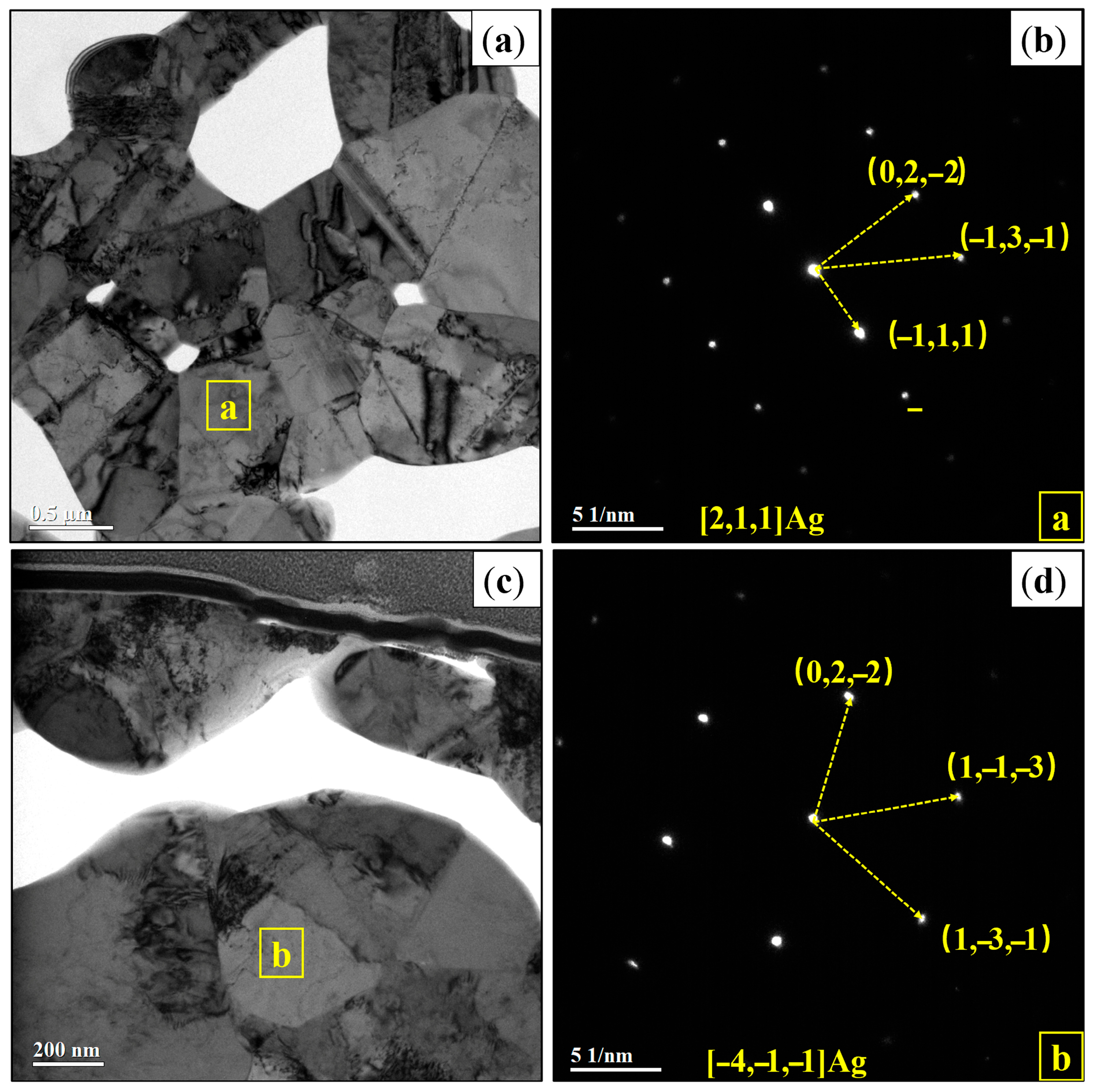
3.2.1. Microstructure and Division of the Sintered Silver

Previous EBSD results revealed that the influence of nanoindentation is more pronounced within approximately 3 µm from the maximum indentation depth along the indentation direction. Based on this, three regions were identified in the cross-section of the nanoindentation sample according to their distance from the indentation site: the region directly below the indentation (≤1 μm), the region at the edge of the indentation (1–3 μm), and the region far away from the indentation (>3 μm).
To systematically investigate the effect of nanoindentation experiments on the microstructure of sintered silver, five representative regions were selected for detailed analysis in this study, as shown in Figure 4. Figure 4a demonstrates the overall preview of the TEM cross-section test, in which the triangle marked the indentation test area and the yellow dashed boxes marked the five representative regions: Region I (within the region directly below the indentation), Region II and Region III (within the region at the edge of the indentation), Region IV and Region V (within the region far away from the indentation). The high-resolution TEM images of these regions are shown in Figure 4b–e, respectively, revealing the microstructural features of each region and demonstrating the gradual attenuation of indentation-induced structural changes.
In this study, the differentiation of the regions is based on the relative position, supplemented by other features. The relative position refers to the spatial location of the cross-section of the sintered silver sample relative to the indentation, while the auxiliary features include microstructural features and diffraction pattern features. This comprehensive differentiation criterion effectively reduces the interference of the microstructural inhomogeneity formed during the sintering process of sintered silver on the experimental results. It enables the study to focus on the mechanism of the influence of the nanoindentation process on the microstructural evolution of sintered silver. The indentation-induced stress field shows a continuous gradient distribution from the center outward, with smooth transitions between regions. In addition, different magnifications were applied in the TEM for the overall and regional images, which supported the existence of the nanoindentation-induced microstructural evolution.
As shown in Figure 4a, sintered silver exhibits two microstructural features: grain structure and pore network. In terms of grains, the sintered silver grains present an irregular polygonal morphology with an uneven grain size distribution, mainly concentrated in the range of 200–1000 nm. The grain boundaries are recognizable, showing a line-like structure with obvious contrast between light and dark, which indicates that a complete grain boundary network was formed during the sintering process. A slight strain contrast was observed at some grain boundaries, which may be related to the residual strain formed during the sintering process. The residual strain mainly stems from thermal stresses during sintering and lattice mismatch between silver nanoparticles. These factors influence subsequent deformation behavior, potentially acting as a dislocation source and affecting the material’s mechanical properties. In terms of pore structure, a distinctive feature of sintered silver is its porous network structure, where the pores are mainly distributed between the grains, presenting irregular shapes with sizes ranging from tens of nanometers to hundreds of nanometers. These pores are the result of the sintering of silver nanoparticles.

3.2.2. Deformation Analysis of the Sintered Silver During Nanoindentation

TEM characterization results of Region I (within the region directly below the indentation) reveal a high-density complex dislocation network structure, indicating that the region directly below the indentation has undergone severe plastic deformation. As shown in Figure 5a, the dislocation density in this region is relatively high and exhibits a complex network-like distribution, indicating that multiple slip systems are activated simultaneously. The dislocation lines were interwoven into a network with variable directions, forming a typical dislocation cell structure, which indicated the stress concentration phenomenon during the indentation deformation process. Figure 5b,c display the SAED images of Region a and Region b. These images correspond to the face-centered cubic (FCC) structure of silver, with crystallographic band axes [2 1 1] and [−1 −1 −1], respectively. This indicates localized lattice rotation and inhomogeneous strain distribution around the indentation. The coexistence of these band axes further confirms the non-uniform strain distribution. The (111) interplanar spacings measured from Region a, Region b, Region c, and Region d are 0.232 nm, 0.237 nm, 0.232 nm, and 0.234 nm, respectively, with an average of 0.23375 nm. Compared to the standard (111) interplanar spacing for silver (0.2359 nm), this represents a microscopic strain of approximately 0.91%, consistent with the deformation caused by direct indentation. The slightly larger (111) interplanar spacing in Region b (0.237 nm) suggests a non-uniform strain distribution, likely related to dislocation activity and localized stress release.
TEM characterization results of Region II and Region III (within the region at the edge of the indentation) reveal more ordered dislocation distribution and lower lattice strain, indicating that the region at the edge of the indentation has undergone less plastic deformation. As shown in Figure 6a,d, the dislocation densities in the region at the edge of the indentation are lower than those in the region directly below the indentation, while higher than those in the region far away from the indentation. The distribution of dislocations is more organized, with most dislocations aligned in a specific direction, forming an obvious slip band structure. This indicates that plastic deformation is mainly realized by a few preferentially oriented slip systems in the edge region of the indentation. The SAED images for Region a, Region b, Region c, and Region d are shown in Figure 6b,c,e,f, respectively. The (111) interplanar spacing was measured for Region a, Region b, and Region c, yielding values of 0.235 nm, 0.236 nm, and 0.235 nm, with an average of 0.2354 nm. This corresponds to a microscopic strain of approximately 0.22% compared to the standard value. This lower strain indicates that the extent of plastic deformation in the region at the edge of the indentation (Region II and Region III) is less than that in the region directly below the indentation (Region I).
TEM characterization results of Region IV and Region V (within the region far away from the indentation) show lower dislocation density and lattice spacing close to standard values, indicating the region far away from the indentation is less affected by the indentation stress field. This region is relatively far away from the center of the indentation, which is less affected by the indentation stress field, as a reference region for the study of the microstructure of sintered silver. As shown in Figure 7a,c, the dislocation densities in Region IV and Region V are low, which are lower than those in the indentation region. Figure 7b,d display the SAED images, confirming the coexistence of [2 1 1] and [−4 −1 −1] band axes. The (111) interplanar spacing is 0.235 nm and 0.236 nm, respectively, with an average value of 0.2355 nm, which is very close to the standard lattice spacing of silver (0.2359 nm), with a deviation of only 0.17%. This indicated that for the region far away from the indentation (Region IV and V), the residual strain remained in the sintered silver. Compared to the region directly below the indentation (Region I), the deviation is only 0.91%. Combined with the analysis of EBSD results, Region IV and V could both serve as references, representing the original state of the sintered silver including the porous network structure, irregular polygonal grains, and initial dislocations of lower density.
SAED images reveal that even in regions far away from the indentation, localized lattice rotation and non-uniform strain distribution exist, which are attributed to the sintering process itself and represent inherent microstructural features of sintered silver. Therefore, this study focuses on the observation of dislocation structure, lattice parameter comparison, and GND density distribution analysis to explain the indentation-induced plastic deformation more effectively. Based on the TEM observation and SAED image analysis, it is clear that the plastic deformation of sintered silver under the action of nanoindentation is mainly realized through the dislocation slip mechanism. In the region directly below the indentation, due to the complex stress state, multiple slip systems are activated at the same time, leading to an extremely high dislocation density and forming a complex dislocation network. In the indentation edge region, the stress state is relatively simple and mainly activates the slip systems along specific directions, forming an orderly dislocation arrangement and distinct slip bands. At the microscopic scale, the dislocation structure observed by TEM is mainly concentrated in the localized region around the indentation, and the dislocation density decreases rapidly with increasing distance from the indentation. This is consistent with the trend of GND density distribution measured by EBSD. In addition, the lattice parameters of different regions were measured and reveal that the lattice microscopic strain decreased with increasing distance from the indentation, further reflecting the spatial distribution characteristics. Combined with the dislocation distribution and lattice strain analyses, it is possible that during nanoindentation, sintered silver initially experiences substantial dislocation slip, forming a complex network structure. Dislocation density diminishes with increasing distance from the indentation, resulting in the observed intricate microstructural features.

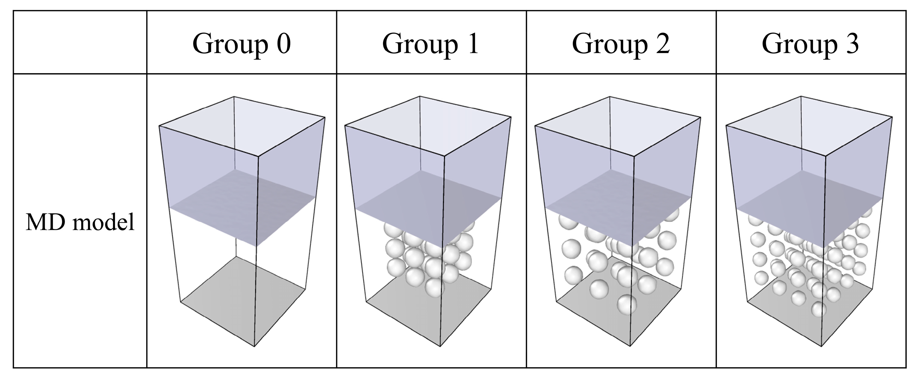
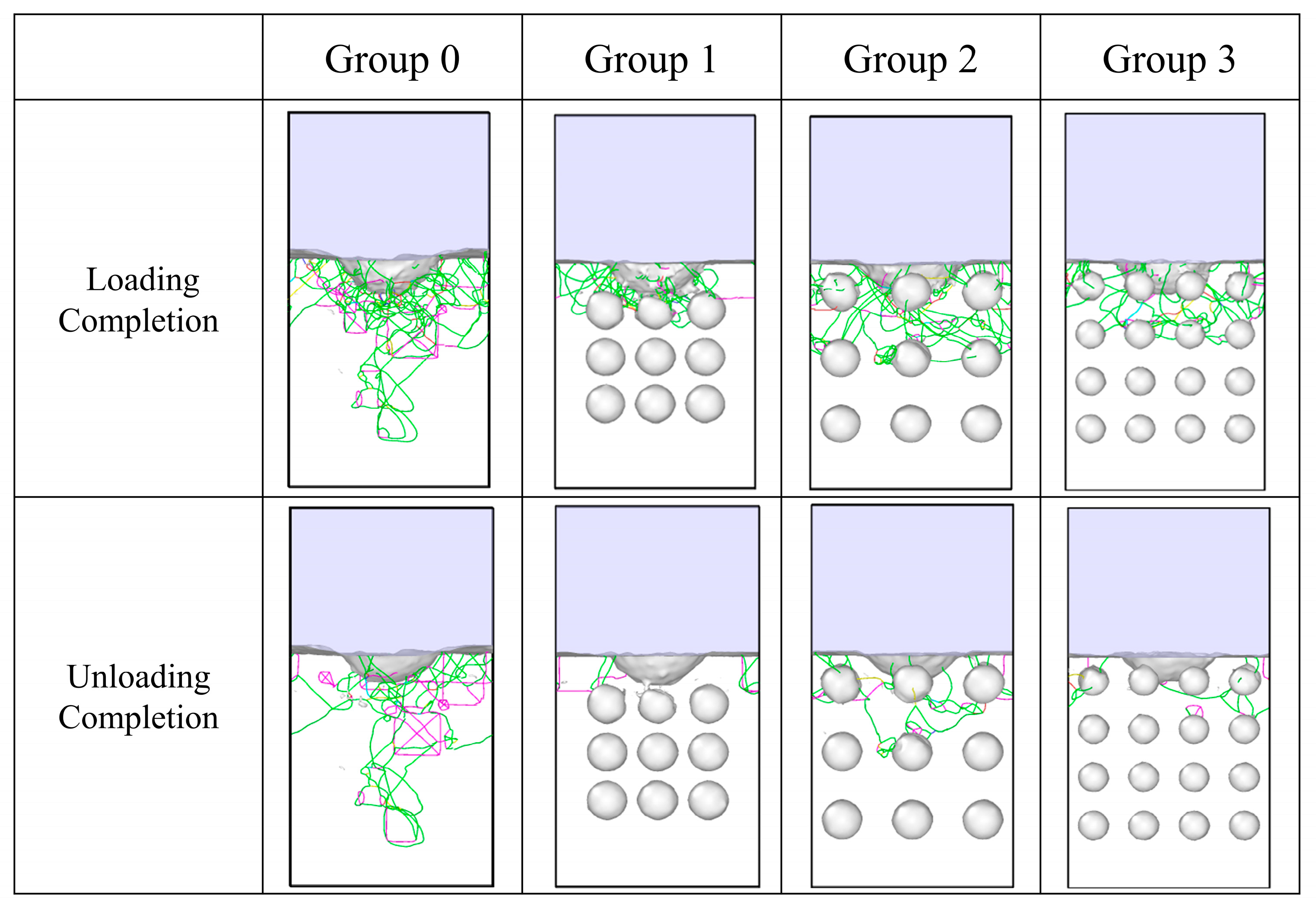
3.3. MD Simulation Results

In this work, MD simulations were carried out to investigate the mechanisms of dislocation formation, evolution, and disappearance during nanoindentation at an atomic scale. Since the size of the indenter and the depth of the indentation in the MD simulation are much smaller than those in the actual experiments, the MD simulations are essentially considered to be an atomic-scale description of the deformation in the very early stages of the nanoindentation. Based on the experimentally measured porosity range of sintered silver (8–33%), four distinct models were designed as shown in Figure 8. As shown in Figure 8, Group 0 represents pore-free monocrystalline silver, while Groups 1–3 have different pore distribution. As shown in Figure 1, the pore configurations are designed to investigate two primary parameters: porosity and average pore size. Group 1 and Group 3 have the same average pore spacing (5 nm) but different porosity (23.7% for Group 1 and 10% for Group 3), enabling the study of how the porosity influences deformation. Meanwhile, Group 2 and Group 3 share the similar porosity (8.6% and 10%) with different average pore size (3.84 nm for Group 2 and 2.88 nm for Group 3), allowing the investigation of the impact of average pore size on deformation behavior under comparable porosity conditions. This parametric design systematically explores how pore distribution characteristics affect dislocation behavior during nanoindentation.
The nanoindentation load–depth curve illustrates the impact of pore distribution on the mechanical response during nanoindentation. Figure 9 presents the averaged load–depth curves with standard deviations for the four models (Groups 0–3), obtained from five independent MD simulations conducted for each configuration. It should be noted that the maximum load correlates directly with the hardness in nanoindentation testing and simulation, due to the surface resistance to plastic deformation [38]. Group 0 has the highest maximum load of 0.46 μN, while Groups 1–3 have lower maximum loads (0.34 μN, 0.39 μN, and 0.43 μN, respectively), demonstrating that the pores reduce the hardness of silver. During nanoindentation, it is observed that the load curve continues to ascend after the sudden load drop until the deformation energy of the subsequent stage is released again. This cyclic pattern represents specific events in the development of dislocation structures during indentation and is consistent with existing research [39], which validates the MD simulation approach. In addition, hysteresis in unloading curves relates to adhesion between the indenter and silver atoms, with varying slopes and residual deformations across models, indicating that pore distribution affects elastic recovery.
Analysis of dislocation configurations across different pore distribution models reveals the influence of pore distribution on dislocation propagation and disappearance during nanoindentation. Figure 10 presents dislocation configurations for the models at loading and unloading completion. The green lines represent the Shockley partial dislocations, blue lines for total dislocations, rose-red lines for compression bar dislocations, yellow lines for Hirth dislocations, and red lines for other types of dislocations. In all groups, the Schottky dislocation (green lines) is the predominant type of dislocation.
EBSD analysis in Section 3.1.2 demonstrates that GND density decreases with distance from the indentation, indicative of an indentation-induced strain gradient. The TEM characterization in Section 3.2.2 confirms this trend and reveals that lattice microscopic strain decreased with increasing distance from the indentation, further supporting the spatial distribution characteristics observed in the MD simulations. As shown in Figure 10, the dislocations form a complex network mainly in the hemispherical area below the indentation, with dislocation density decreasing with distance from the indentation, consistent with the EBSD findings and TEM observations. Specifically, the MD simulation results demonstrate the same decreasing trend of defect density with distance as observed in the EBSD analysis and TEM observations, validating the reliability of the computational approach and confirming the indentation-induced strain gradient mechanism at the atomic scale.
As shown in Figure 10, distinct dislocation behaviors are observed across different pore distribution. Group 0 (pore-free) exhibits extensive dislocation networks throughout the material during loading and substantial remaining dislocations after unloading. It indicated the plastic deformation and the limited elastic recovery. The dislocation density in the pore-containing models (Groups 1–3) is clearly lower than in the pore-free model (Group 0), demonstrating that pores overall suppress dislocation propagation. In Group 1, fewer dislocations mainly concentrate in narrow regions between pores. Most dislocations disappear after unloading, with only a small number remaining, demonstrating better elastic recovery. Group 2 has more dislocations than Group 3, with a broader distribution due to increased pore spacing, allowing more dislocation movement. A portion of dislocations, particularly around pores, remain after unloading, confirming that the dislocations are pinned by pores.
Quantitative analysis of the total length of dislocation further reveals the influence of pore distribution on dislocation behavior during nanoindentation. Figure 11 compares the total dislocation length across different models based on statistical analysis of five independent simulation runs for each group. At loading completion, Group 0 exhibits the longest total dislocation length (7751.06 ± 1006.71 nm), while Group 1 shows the shortest (2263.14 ± 462.24 nm), with Group 2 and Group 3 at 5946.57 ± 403.77 nm and 3687.85 ± 391.64 nm, respectively. Comparing Group 3 and Group 1, the porosity increases from 10% to 23.7%, leading to a 63% decrease in total dislocation length, indicating that higher porosity restricts dislocation propagation due to the blocking effect of pores. Comparing Group 2 and Group 3, while maintaining similar porosity (8.6% vs. 10%), the average pore size decreases from 3.84 nm to 2.88 nm, leading to a 38% increase in total dislocation length. This indicates that smaller, more evenly dispersed pores enhance dislocation propagation.
After unloading, the total dislocation length decreases across all models: Group 0 decreases by 22% to 6042.53 ± 828.45 nm, Group 1 by 67% to 752.34 ± 190.02 nm, Group 2 by 39% to 3650.71 ± 601.41 nm, and Group 3 by 70% to 1091.23 ± 560.74 nm. This indicates that pore distribution affects the dislocation annihilation, thereby enhancing elastic recovery capabilities. Groups 1 and 3 achieve similar high dislocation disappearance rates (67% and 70%, respectively) through different mechanisms. Group 1 benefits from high porosity (23.7%) that provides abundant pore–matrix interfaces for dislocation annihilation, while Group 3 benefits from smaller average pore size (2.88 nm) that creates more uniformly distributed annihilation sites. Comparing Group 2 and Group 3, while maintaining similar porosity (8.6% vs. 10%), the average pore size decreases from 3.84 nm to 2.88 nm, leading to a 31% increase in dislocation disappearance rate from 39% to 70%. This indicates that smaller and more evenly dispersed pores could enhance the dislocation annihilation efficiency, further promoting the elastic recovery.
This MD method provides quantitative insights into the relationship between the pore microstructure and the dislocation behavior in sintered silver, establishing a foundation for optimizing pore distribution to enhance mechanical properties. Further work could focus on investigating the effects of pore shape and connectivity on deformation mechanisms, as well as extending the analysis to different loading conditions and strain rates.

4. Conclusions

This study combines experimental characterization (SEM, EBSD, and TEM) with MD simulations to investigate the deformation mechanisms of pressureless sintered silver during nanoindentation. The following conclusions are drawn:
  • SEM characterization reveals that the sintered silver sample enabled a typical porous network structure with a porosity of 8% to 33%, which was further set as key parameters for subsequent MD simulations.
  • EBSD characterizations reveal that sintered silver under nanoindentation exhibited localized plastic deformation, which was closely related to the porous network structure. The pore both promoted dislocation formation and restricted dislocation motion, leading to the observed GND density distribution.
  • TEM characterization revealed distinct regional variations in microstructural evolution following nanoindentation. By examining dislocation structures and comparing lattice parameters, this study explored the mechanisms of nanoindentation-induced plastic deformation. The findings indicated that during nanoindentation, sintered silver initially experienced substantial dislocation slip, forming a complex network structure. Dislocation density diminished with increasing distance from the indentation.
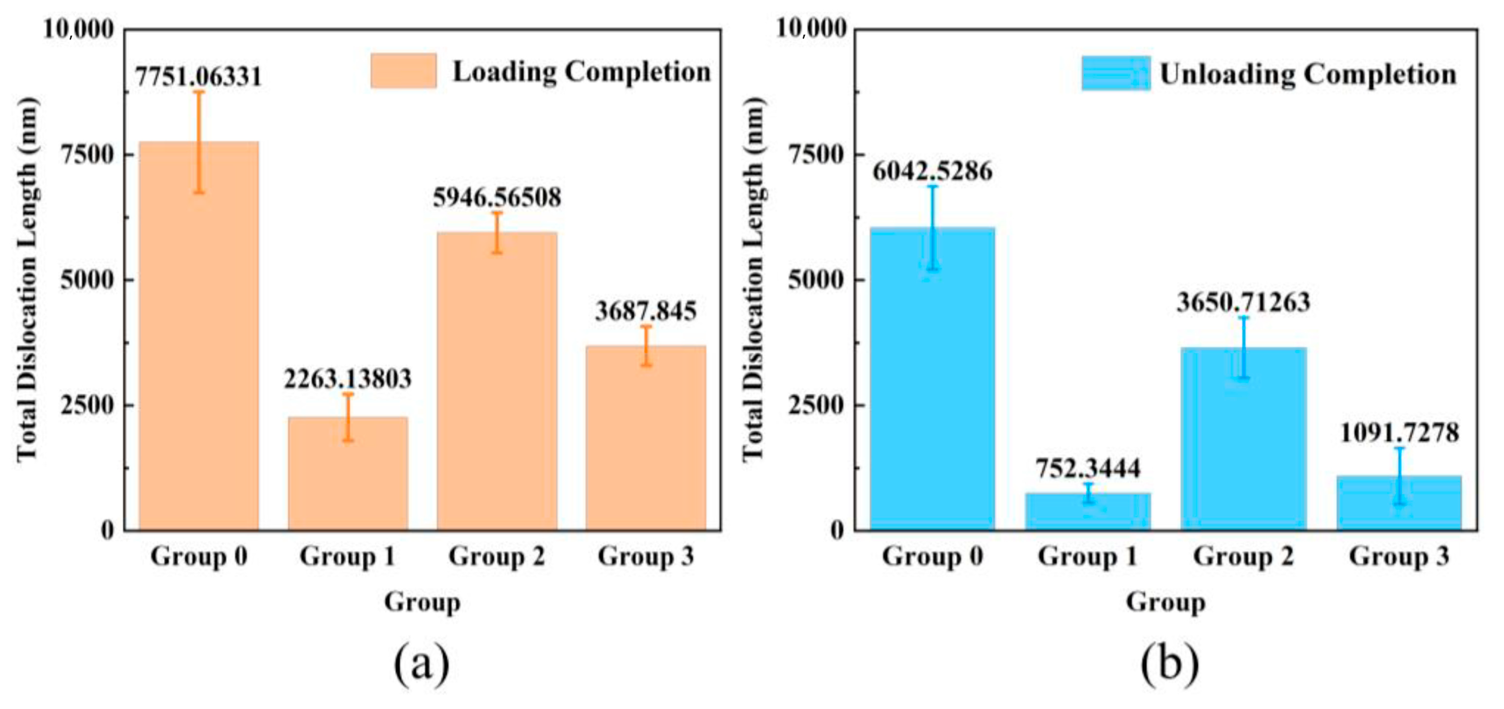
  • MD simulation results showed that the dislocation density decreased with distance from the indentation test point, which corroborated the EBSD and TEM experimental findings. Quantitative analysis further revealed that the total dislocation length was influenced by the pore parameters, namely porosity and the average pore size. During loading, the total dislocation length was reduced by 63% with a 13.7% increase in porosity (from 10% to 23.7%). When the average pore size decreased from 3.84 nm to 2.88 nm, it led to a 38% increase in the total dislocation length. During unloading, it is found that the smaller average pore size (from 3.84 nm to 2.88 nm) enhanced the dislocation disappearance rate by 31% (from 39% to 70%). Higher porosity provides abundant pore–matrix interfaces for dislocation annihilation, while smaller average pore size creates more uniformly distributed annihilation sites. Pores could alter the dislocation propagation pathways, thus affecting the dislocation nucleation and annihilation processes, which leads to the influence on mechanical response during nanoindentation.
This integrated experimental and simulation approach promotes the understanding of the deformation mechanisms of sintered silver during nanoindentation, highlighting the interplay between porosity and dislocation dynamics. This work not only advances the understanding of porous metallic materials under nanoindentation tests but also provides insights for optimizing sintered silver microstructures in high-performance electronic applications.

Author Contributions

Conceptualization, Y.S.; methodology, Y.S.; software, Y.S.; validation, Y.S.; formal analysis, Y.S.; investigation, Y.S.; resources, P.L., X.W. and H.C.; data curation, Y.S.; writing—original draft preparation, Y.S.; writing—review and editing, P.L. and Y.S.; visualization, Y.S.; supervision, P.L.; project administration, P.L.; funding acquisition, P.L. All authors have read and agreed to the published version of the manuscript.

Funding

This research was funded by the National Natural Science Foundation of China under Grant 62304051, Shanghai Science & Technology Commission under Grant 24500790700, and Shanghai SiC Power Devices Engineering & Technology Research Center (19DZ2253400).

Data Availability Statement

The original contributions presented in this study are included in the article. Further inquiries can be directed to the corresponding author.

Acknowledgments

In this work, the authors would like to thank Heraeus Materials Technology Shanghai Ltd. for prototype validation and characterization support. During the preparation of this study, the authors used GenAi for the purpose of polishing the article. The authors have reviewed and edited the output and take full responsibility for the content of this publication.

Conflicts of Interest

The authors declare no conflicts of interest.

Abbreviations

The following abbreviations are used in this manuscript:
EBSDElectron Backscatter Diffraction
SAEDSelected Area Electron Diffraction
PEGPolyethylene Glycol
SEMScanning Electron Microscope
TEMTransmission Electron Microscopy
GNDGeometrically Necessary Dislocation
MDMolecular Dynamics

References

  1. Matallana, A.; Ibarra, E.; López, I.; Andreu, J.; Garate, J.I.; Jordà, X.; Rebollo, J. Power module electronics in HEV/EV applications: New trends in wide-bandgap semiconductor technologies and design aspects. Renew. Sustain. Energy Rev. 2019, 113, 109264. [Google Scholar] [CrossRef]
  2. Roccaforte, F.; Alquier, D.; Kimoto, T.; Agarwal, A. Silicon Carbide materials and devices: Power electronics and innovative applications. Mater. Sci. Semicond. Process. 2024, 182, 108675. [Google Scholar] [CrossRef]
  3. Ngwashi, D.K.; Luong Viet, P. Recent review on failures in silicon carbide power MOSFETs. Microelectron. Reliab. 2021, 123, 114169. [Google Scholar] [CrossRef]
  4. Wang, X.; Chen, H.; Yang, Z.; Liu, W.; Zeng, Z.; Zhang, G.; Zhang, J.; Fan, J.; Liu, P. Microstructure evolution and micromechanical behavior of solvent-modified Cu–Ag composite sintered joints for power electronics packaging at high temperatures. J. Mater. Res. Technol. 2024, 30, 8433–8450. [Google Scholar] [CrossRef]
  5. Yan, H.; Liang, P.; Mei, Y.; Feng, Z. Progress and Considerations on Pressure-less Low-temperature Sintering of Nano-silver for Packaging Power Electronic Devices. J. Power Supply 2020, 18, 15–23. [Google Scholar]
  6. Peng, P.; Hu, A.; Gerlich, A.P.; Zou, G.; Liu, L.; Zhou, Y.N. Joining of Silver Nanomaterials at Low Temperatures: Processes, Properties, and Applications. ACS Appl. Mater. Interfaces 2015, 7, 12597–12618. [Google Scholar] [CrossRef] [PubMed]
  7. Won, M.; Kim, D.; Yang, H.; Oh, C. Low-Temperature Sinterable Cu@Ag Paste with Superior Strength Driven by Pre-Heating Process. Energies 2023, 16, 5419. [Google Scholar] [CrossRef]
  8. Song, R.; Yuan, F.; Su, Y.; Wang, S.; Zhang, X. Infrared Radiation-Assisted Non-Pressure Sintering of Micron-Sized Silver for Power Electronic Packaging. Electronics 2024, 13, 1492. [Google Scholar] [CrossRef]
  9. Agyakwa, P.A.; Robertson, S.; Dai, J.; Mouawad, B.; Zhou, Z.; Liu, C.; Johnson, C.M. Microstructural Response of Highly Porous Sintered Nano-silver Particle Die Attachments to Thermomechanical Cycling. J. Electron. Mater. 2024, 53, 1561–1576. [Google Scholar] [CrossRef]
  10. Chen, C.; Suganuma, K. Microstructure and mechanical properties of sintered Ag particles with flake and spherical shape from nano to micro size. Mater. Des. 2019, 162, 311–321. [Google Scholar] [CrossRef]
  11. Liu, J.; Lv, W.; Chen, C.; Kang, Y. Atomic insight in fusion mechanism of heterogeneous and homogeneous sintering: Cu and Ag nanoparticles. Results Phys. 2024, 57, 107411. [Google Scholar] [CrossRef]
  12. Wang, N.; Si, X.; Zhang, B.; Gao, J.; Li, M.; Lin, T.; Li, R.; Li, C.; Qi, J.; Cao, J. Micro-Ag particle interlayer with high dislocation density for sintered-joining of Al2O3 and AlN in air. Ceram. Int. 2024, 50 Pt A, 29153–29168. [Google Scholar] [CrossRef]
  13. Chen, C.; Choe, C.; Kim, D.; Zhang, Z.; Long, X.; Zhou, Z.; Wu, F.; Suganuma, K. Effect of oxygen on microstructural coarsening behaviors and mechanical properties of Ag sinter paste during high-temperature storage from macro to micro. J. Alloys Compd. 2020, 834, 155173. [Google Scholar] [CrossRef]
  14. Wang, J.; Yodo, S.; Tatsumi, H.; Nishikawa, H. Reliability-enhanced microscale Ag sintered joint doped with AlN nanoparticles. Mater. Lett. 2023, 349, 134845. [Google Scholar] [CrossRef]
  15. Ma, Y.; Li, X.; Zhang, H. Effect of Grain Structure of Gold Plating Layer on Environmental Reliability of Sintered Ag-Au Joints. Materials 2024, 17, 1844. [Google Scholar] [CrossRef]
  16. Li, W.; Chen, C.; Nishijima, M.; Ueshima, M.; Nishikawa, H.; Suganuma, K. Improved thermal shock reliability of Ag paste sintered joint by adjusted coefficient of thermal expansion with Ag-Si atomized particles addition. Mater. Des. 2024, 246, 113308. [Google Scholar] [CrossRef]
  17. Borysiuk, V.; Lyashenko, I.A.; Popov, V.L. Molecular Dynamics Study of Friction between Ag Nanoparticle and Two-Dimensional Titanium Carbide Ti2C (MXene). Crystals 2024, 14, 272. [Google Scholar] [CrossRef]
  18. Long, X.; Guo, Y.; Su, Y.; Siow, K.S.; Chen, C. Constitutive, creep, and fatigue behavior of sintered Ag for finite element simulation of mechanical reliability: A critical review. J. Mater. Sci.-Mater. Electron. 2022, 33, 2293–2309. [Google Scholar] [CrossRef]
  19. Yang, F.; Liu, S.; Zhou, Z.; Chen, Z.; Liu, L.; Liu, C.; Liu, C. Mechanical properties of intermetallic compounds at elevated temperature by nanoindentation. In Proceedings of the 2019 IEEE 69TH Electronic Components and Technology Conference (ECTC), Las Vegas, NV, USA, 28 May 2019; pp. 850–854. [Google Scholar]
  20. Song, E.; Andani, M.T.; Misra, A. Investigation of grain size and geometrically necessary dislocation density dependence of flow stress in Mg-4Al by using nanoindentation. Acta Mater. 2024, 265, 119633. [Google Scholar] [CrossRef]
  21. Wu, Y.; Zou, G.; Wang, S.; Guo, W.; Zhang, H.; Liu, L. Interfacial bonding mechanisms of sintered Cu nanoparticles on different metallization surfaces. Surf. Interfaces 2024, 46, 104173. [Google Scholar] [CrossRef]
  22. Xu, Y.; Zhou, Z.; Dong, M.; Zhou, W.; Nomura, N. SiC nanofiber-reinforced Ag matrix composites exhibiting high strength and ductility. Mater. Sci. Eng. A 2024, 916, 147352. [Google Scholar] [CrossRef]
  23. Zou, T.; Wu, T.; Lang, Z.; Wang, W.; Ye, Z.; Yang, J.; Huang, J. Microstructure and failure behavior of polycrystalline joint with near composition to the base material of single crystal superalloy with large orientation deviation. Eng. Fail. Anal. 2025, 170, 109249. [Google Scholar] [CrossRef]
  24. Wang, D.; Zhang, Z.; Liu, D.; Deng, X.; Shi, C.; Gu, Y.; Liu, X.; Liu, X.; Wen, W. The damage mechanism in copper studied using in situ TEM nanoindentation. Nanoscale Adv. 2024, 6, 2002–2012. [Google Scholar] [CrossRef]
  25. Lai, Y.-C.; Ying, Y.; Yadav, D.; Guerrero, J.; Hu, Y.-J.; Xie, K.Y. In situ TEM observations and molecular dynamics simulations of deformation defect activities in Mg via nanoindentation. J. Magnes. Alloys 2023, 11, 4513–4524. [Google Scholar] [CrossRef]
  26. Long, X.; Jia, Q.; Shen, Z.; Liu, M.; Guan, C. Strain rate shift for constitutive behaviour of sintered silver nanoparticles under nanoindentation. Mech. Mater. 2021, 158, 103881. [Google Scholar] [CrossRef]
  27. Tang, P.; Feng, J.; Wan, Z.; Huang, X.; Yang, S.; Lu, L.; Zhong, X. Influence of grain orientation on hardness anisotropy and dislocation behavior of AlN ceramic in nanoindentation. Ceram. Int. 2021, 47, 20298–20309. [Google Scholar] [CrossRef]
  28. Xu, Y.; Qiu, X.; Li, W.; Wang, S.; Ma, N.; Ueshima, M.; Chen, C.; Suganuma, K. Development of high thermal conductivity of Ag/diamond composite sintering paste and its thermal shock reliability evaluation in SiC power modules. J. Mater. Res. Technol. 2023, 26, 1079–1093. [Google Scholar] [CrossRef]
  29. Chamma, L.; Pipard, J.-M.; Arlazarov, A.; Richeton, T.; Lecomte, J.-S.; Berbenni, S. A combined EBSD/nanoindentation study of dislocation density gradients near grain boundaries in a ferritic steel. Mater. Tech. 2022, 110, 203. [Google Scholar] [CrossRef]
  30. Chamma, L.; Pipard, J.-M.; Arlazarov, A.; Richeton, T.; Berbenni, S. A plasticity-induced internal length mean field model based on statistical analyses of EBSD and nanoindentation data. Int. J. Plast. 2025, 189, 104327. [Google Scholar] [CrossRef]
  31. Javaid, F.; Xu, Y.; Bruder, E.; Durst, K. Indentation size effect in tungsten: Quantification of geometrically necessary dislocations underneath the indentations using HR-EBSD. Mater. Charact. 2018, 142, 39–42. [Google Scholar] [CrossRef]
  32. Dziaszyk, S.; Payton, E.J.; Friedel, F.; Marx, V.; Eggeler, G. On the characterization of recrystallized fraction using electron backscatter diffraction: A direct comparison to local hardness in an IF steel using nanoindentation. Mater. Sci. Eng. A-Struct. Mater. Prop. Microstruct. Process. 2010, 527, 7854–7864. [Google Scholar] [CrossRef]
  33. Calcagnotto, M.; Ponge, D.; Demir, E.; Raabe, D. Orientation gradients and geometrically necessary dislocations in ultrafine grained dual-phase steels studied by 2D and 3D EBSD. Mater. Sci. Eng. A-Struct. Mater. Prop. Microstruct. Process. 2010, 527, 2738–2746. [Google Scholar] [CrossRef]
  34. De Vincentis, N.S.; Field, D.P. Factors affecting Confidence Index in EBSD analysis. Ultramicroscopy 2021, 225, 113269. [Google Scholar] [CrossRef] [PubMed]
  35. Wang, X.; Wang, X.; Liu, M.; Wang, Y. Melting suspending of Ag nano-particles monitored by molecular dynamics simulation. Chem. Phys. 2019, 527, 110459. [Google Scholar] [CrossRef]
  36. Zhu, P.; Hu, Y.; Wang, H. Molecular dynamics simulations of atomic-scale friction in diamond-silver sliding system. Chin. Sci. Bull. 2009, 54, 4555–4559. [Google Scholar] [CrossRef]
  37. Goel, S.; Cross, G.; Stukowski, A.; Gamsjaeger, E.; Beake, B.; Agrawal, A. Designing nanoindentation simulation studies by appropriate indenter choices: Case study on single crystal tungsten. Comput. Mater. Sci. 2018, 152, 196–210. [Google Scholar] [CrossRef]
  38. Zhao, J.; Zhang, Y.; Cui, C.; Wang, B. Insights into nanomechanical behavior of ettringite: Simulations of nanoindentation based on molecular dynamics. Mater. Today Commun. 2025, 43, 111637. [Google Scholar] [CrossRef]
  39. Mes-adi, H.; Lablali, M.; Ait ichou, M.; Ou-khouya, A.; Tahiri, M.; Saadouni, K.; Mazroui, M. Atomistic insight of deformation mechanisms and mechanical characteristics of nano-scale silver (100) using nanoindentation. Mater. Today Commun. 2024, 40, 110086. [Google Scholar] [CrossRef]
Figure 1. Schematic diagram of MD simulation and experimental procedures: (a) XZ Plane of the MD Model; (b) XY Plane of the MD Model.
Crystals 15 00620 g001
Figure 2. Representative SEM images and porosity of the sintered silver samples.
Crystals 15 00620 g002
Figure 3. EBSD results of the nanoindentation cross-section of sintered silver: (a) GND density distribution; (b) GND density statistical histogram.
Crystals 15 00620 g003
Figure 4. TEM microscopic structure division diagram of the sintered silver indentation area: (a) overall preview and region division; (b) Region I; (c) Region II; (d) Region III and Region IV; (e) Region V.
Crystals 15 00620 g004
Figure 5. TEM and SAED images of Region I (Yellow a–d Indicate Randomly Selected Points for SEAD and Interplanar Spacing Calculations, Consistently Marked in Subsequent Figure 6 and Figure 7): (a) TEM BF image of Region I; (b,c) SAED images of Region a and Region b.
Crystals 15 00620 g005
Figure 6. TEM and SAED images of Region II and Region III: (a) TEM BF image of Region II; (b,c) SAED images of Region a and Region b; (d) TEM BF image of Region III; (e,f) SAED images of Region c and Region d.
Crystals 15 00620 g006
Figure 7. TEM and SAED images of Region IV and Region V: (a) TEM BF image of Region IV; (b) SAED image of Region a; (c) TEM BF image of Region V; (d) SAED image of Region b.
Crystals 15 00620 g007
Figure 8. MD models of monocrystalline silver (001) with different pore distributions for nanoindentation simulation (Group 0: no pores; Groups 1–3: various pore distribution).
Crystals 15 00620 g008
Figure 9. Indentation load–depth curve of monocrystalline silver (001) with different pore distribution for nanoindentation simulation (Group 0: no pores; Groups 1–3: various pore distribution).
Crystals 15 00620 g009
Figure 10. Dislocation configurations at loading and unloading completion during nanoindentation of monocrystalline silver (001) under different pore distribution (Group 0: no pores; Groups 1–3: various pore distribution).
Crystals 15 00620 g010
Figure 11. Total length of dislocation at (a) loading and (b) unloading completion during nanoindentation of monocrystalline silver (001) under different pore distribution (Group 0: no pores; Groups 1–3: various pore distribution).
Crystals 15 00620 g011
Disclaimer/Publisher’s Note: The statements, opinions and data contained in all publications are solely those of the individual author(s) and contributor(s) and not of MDPI and/or the editor(s). MDPI and/or the editor(s) disclaim responsibility for any injury to people or property resulting from any ideas, methods, instructions or products referred to in the content.

