
Electronic Quality Enhancement of Multicrystalline Silicon via SiNx and H2 Plasma Passivation Using Plasma-Enhanced Chemical Vapor Deposition for Photovoltaic Applications


 and
and
Abstract
1. Introduction
2. Materials and Methods
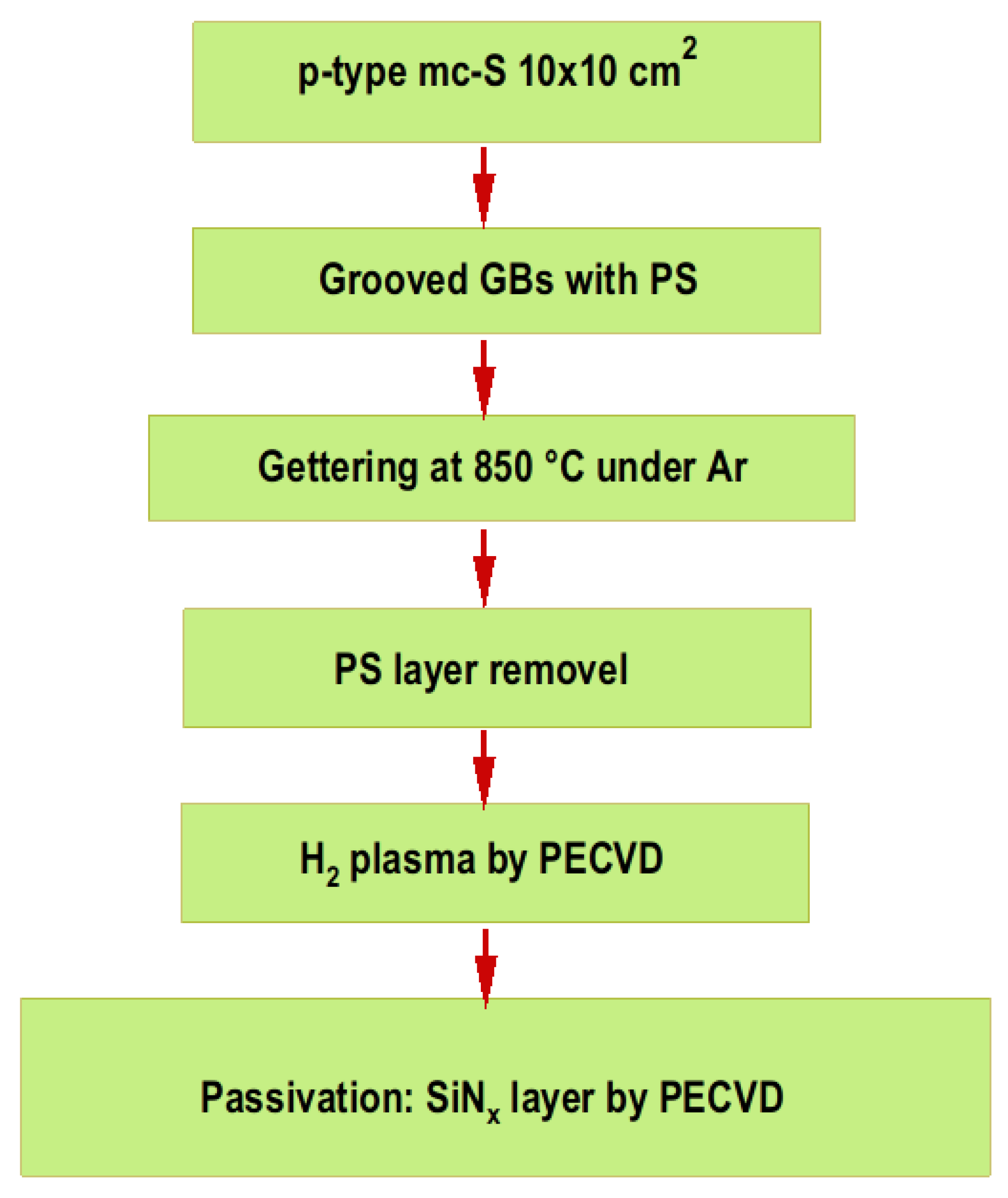
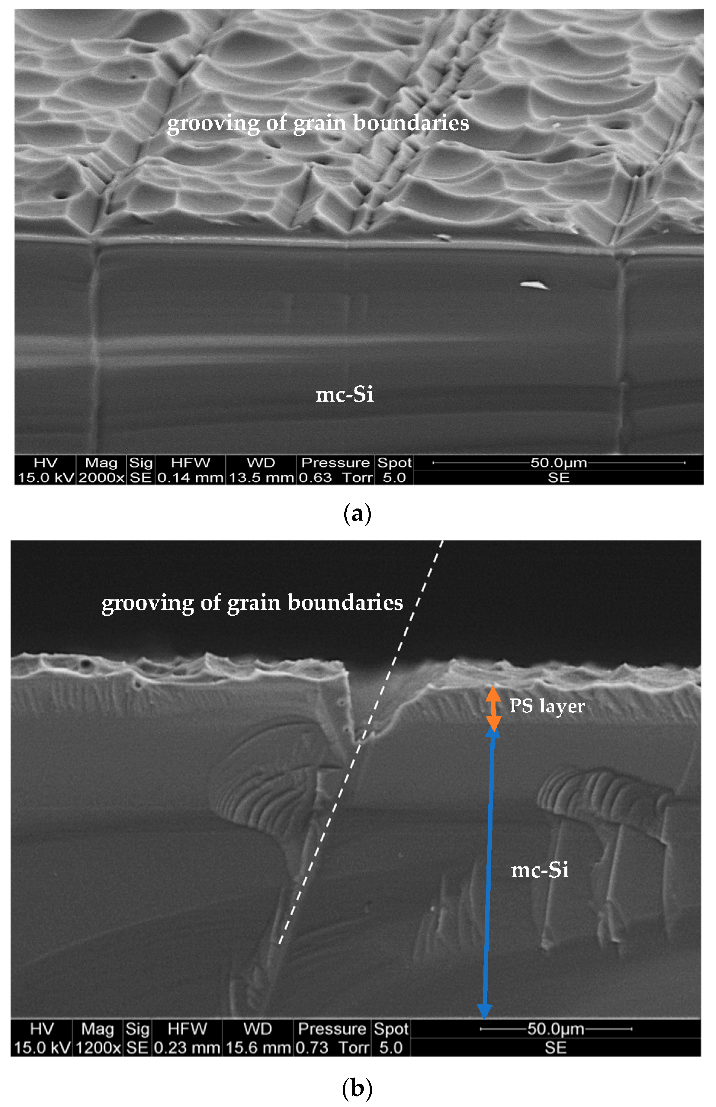
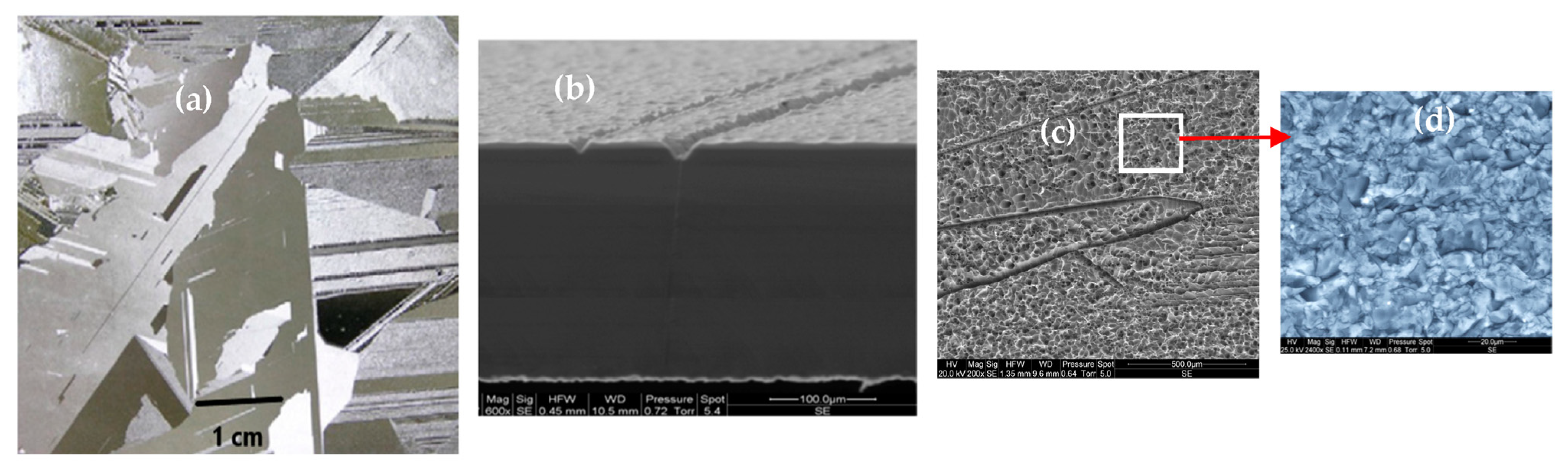
2.1. Sample Preparation for the PECVD Process
2.2. PECVD Application
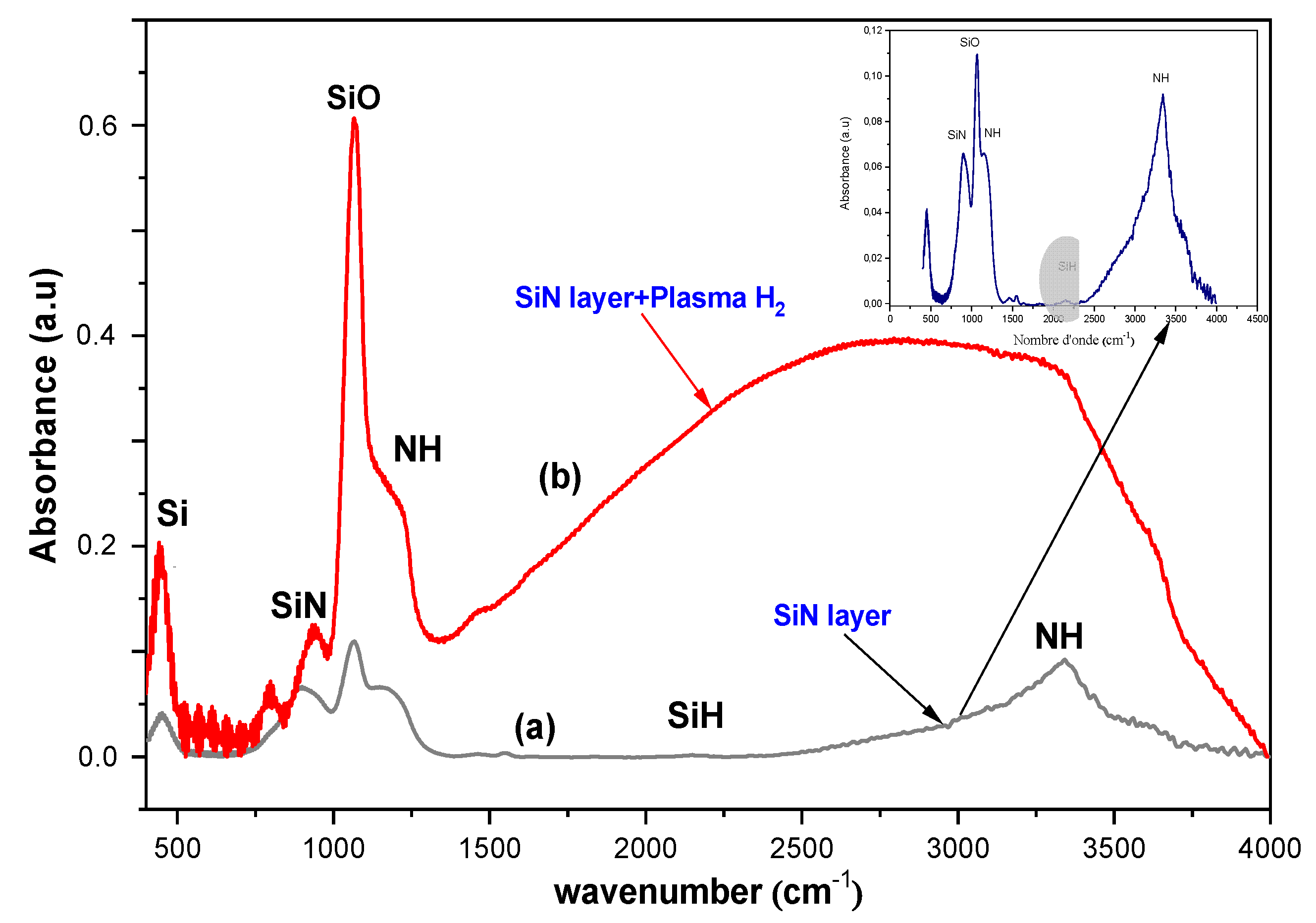
2.3. Characterization Tools
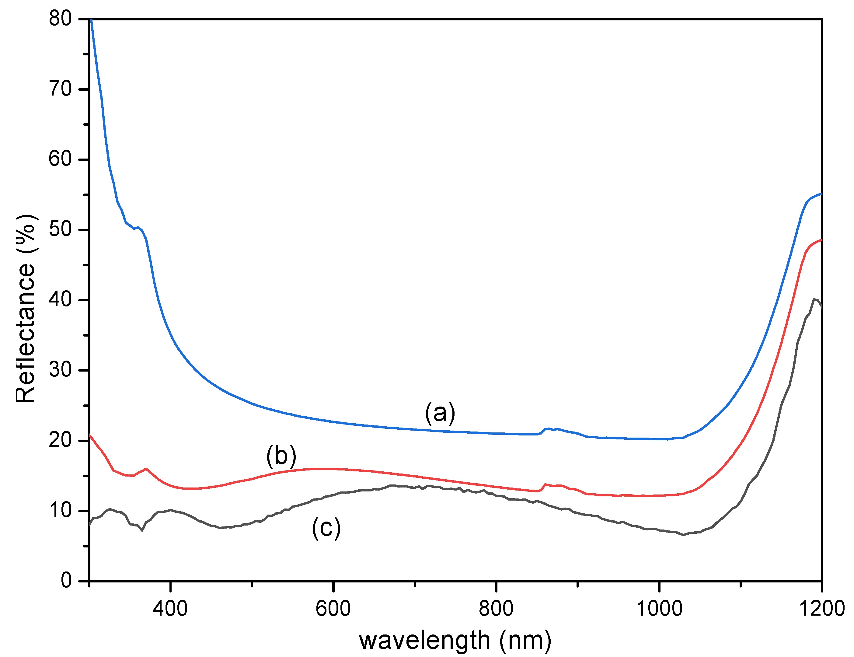
3. Results and Discussion
4. Conclusions
Author Contributions
Funding
Data Availability Statement
Conflicts of Interest
References
- Yu, H.J.J.; Geoffron, P. Solar PV market and policies. In Photovoltaic Solar Energy Conversion; Academic Press: Cambridge, MA, USA, 2020; pp. 413–437. [Google Scholar]
- Allouhi, A.; Rehman, S.; Buker, M.S.; Said, Z. Up-to-date literature review on Solar PV systems: Technology progress, market status and R&D. J. Clean. Prod. 2022, 362, 132339. [Google Scholar]
- Hoffmann, W. PV solar electricity industry: Market growth and perspective. Sol. Energy Mater. Sol. Cells 2006, 90, 3285–3311. [Google Scholar] [CrossRef]
- Jäger-Waldau, A. Snapshot of photovoltaics—March 2025. EPJ Photovolt. 2025, 16, 22. [Google Scholar] [CrossRef]
- Ding, H.; Zhou, D.Q.; Liu, G.Q.; Zhou, P. Cost reduction or electricity penetration: Government R&D-induced PV development and future policy schemes. Renew. Sustain. Energy Rev. 2020, 124, 109752. [Google Scholar]
- Ballif, C.; Haug, F.J.; Boccard, M.; Verlinden, P.J.; Hahn, G. Status and perspectives of crystalline silicon photovoltaics in research and industry. Nat. Rev. Mater. 2022, 7, 597–616. [Google Scholar] [CrossRef]
- Di Sabatino, M.; Hendawi, R.; Garcia, A.S. Silicon solar cells: Trends, manufacturing challenges, and AI perspectives. Crystals 2024, 14, 167. [Google Scholar] [CrossRef]
- Fraunhofer Institute for Solar Energy Systems, ISE. Photovoltaics Report; ISE: Freiburg, Germany, 2023. [Google Scholar]
- Green, M.A.; Dunlop, E.D.; Hohl-Ebinger, J.; Yoshita, M.; Kopidakis, N.; Bothe, K.; Hinken, D.; Rauer, M.; Hao, X. Solar cell efficiency tables (Version 60). Prog. Photovolt. Res. Appl. 2022, 30, 687–701. [Google Scholar] [CrossRef]
- Ogundipe, O.B.; Okwandu, A.C.; Abdulwaheed, S.A. Recent advances in solar photovoltaic technologies: Efficiency, materials, and applications. GSC Adv. Res. Rev. 2024, 20, 159–175. [Google Scholar] [CrossRef]
- Vodapally, S.N.; Ali, M.H. A comprehensive review of solar photovoltaic (PV) technologies, architecture, and its applications to improved efficiency. Energies 2022, 16, 319. [Google Scholar] [CrossRef]
- Yamaguchi, M.; Masuda, T.; Araki, K.; Sato, D.; Lee, K.H.; Kojima, N.; Yamazaki, M. Development of high-efficiency and low-cost solar cells for PV-powered vehicles application. Prog. Photovolt. Res. Appl. 2021, 29, 684–693. [Google Scholar] [CrossRef]
- Yamaguchi, M.; Dimroth, F.; Geisz, J.F.; Ekins-Daukes, N.J. Multi-junction solar cells paving the way for super high-efficiency. J. Appl. Phys. 2021, 129, 240901. [Google Scholar] [CrossRef]
- Green, M.A.; Bremner, S.P. Energy conversion approaches and materials for high-efficiency photovoltaics. Nat. Mater. 2017, 16, 23–34. [Google Scholar] [CrossRef]
- Ashraf, M.; Ayaz, M.; Khan, M.; Adil, S.F.; Farooq, W.; Ullah, N.; Nawaz Tahir, M. Recent trends in sustainable solar energy conversion technologies: Mechanisms, prospects, and challenges. Energy Fuels 2023, 37, 6283–6301. [Google Scholar] [CrossRef]
- Yu, W.; Xue, Y.; Mei, J.; Zhou, X.; Xiong, M.; Zhang, S. Segregation and removal of transition metal impurities during the directional solidification refining of silicon with Al-Si solvent. J. Alloys Compd. 2019, 805, 198–204. [Google Scholar] [CrossRef]
- Lv, X.; Li, H.; Ding, D.; Yu, X.; Jin, C.; Yang, D. Interfacial characterization of non-metal precipitates at grain boundaries in cast multicrystalline silicon crystals. J. Cryst. Growth 2025, 652, 128042. [Google Scholar] [CrossRef]
- Wang, L.; Liu, J.; Li, Y.; Wei, G.; Li, Q.; Fan, Z.; He, D. Dislocations in Crystalline Silicon Solar Cells. Adv. Energy Sustain. Res. 2024, 5, 2300240. [Google Scholar] [CrossRef]
- Yoon, Y.; Yang, W.C.D.; Ha, D.; Haney, P.M.; Hirsch, D.; Yoon, H.P.; Zhitenev, N.B. Unveiling defect-mediated charge-carrier recombination at the nanometer scale in polycrystalline solar cells. ACS Appl. Mater. Interfaces 2019, 11, 47037–47046. [Google Scholar] [CrossRef]
- Dasilva-Villanueva, N.; Catalán-Gómez, S.; Marrón, D.F.; Torres, J.J.; García-Corpas, M.; del Cañizo, C. Reduction of trapping and recombination in upgraded metallurgical grade silicon: Impact of phosphorous diffusion gettering. Sol. Energy Mater. Sol. Cells 2022, 234, 111410. [Google Scholar] [CrossRef]
- Kwak, J.I.; Nam, S.H.; Kim, L.; An, Y.J. Potential environmental risk of solar cells: Current knowledge and future challenges. J. Hazard. Mater. 2020, 392, 122297. [Google Scholar] [CrossRef]
- Achref, M.; Khezami, L.; Mokraoui, S.; Rabha, M.B. Effective surface passivation on multi-crystalline silicon using aluminum/porous silicon nanostructures. Surf. Interfaces 2020, 18, 100391. [Google Scholar] [CrossRef]
- Rabha, M.B.; Salem, M.; El Khakani, M.A.; Bessais, B.; Gaidi, M. Monocrystalline silicon surface passivation by Al2O3/porous silicon combined treatment. Mater. Sci. Eng. B 2013, 178, 695–697. [Google Scholar] [CrossRef]
- Khezami, L.; Jemai, A.B.; Alhathlool, R.; Rabha, M.B. Electronic quality improvement of crystalline silicon by stain etching-based PS nanostructures for solar cells application. Sol. Energy 2016, 129, 38–44. [Google Scholar] [CrossRef]
- Ullah, N.; Ahmad, A.; Sarfaraz, R.; Khalid, S.; Ali, I.; Younas, M.; Rezakazemi, M. Challenges and solutions in solar photovoltaic technology life cycle. ChemBioEng Rev. 2023, 10, 541–584. [Google Scholar] [CrossRef]
- Alrasheedi, N.H. The effects of porous silicon and silicon nitride treatments on the electronic qualities of multicrystalline silicon for solar cell applications. Silicon 2024, 16, 1765–1773. [Google Scholar] [CrossRef]
- Almeshaal, M.A.; Abdouli, B.; Choubani, K.; Khezami, L.; Rabha, M.B. Study of porous silicon layer effect in optoelectronics properties of multi-crystalline silicon for photovoltaic applications. Silicon 2023, 15, 6025–6032. [Google Scholar] [CrossRef]
- Maruska, H.P.; Ghosh, A.K.; Rose, A.; Feng, T. Hall mobility of polycrystalline silicon. Appl. Phys. Lett. 1980, 36, 381–383. [Google Scholar] [CrossRef]
- Liu, A.; Sun, C.; Sio, H.C.; Zhang, X.; Jin, H.; Macdonald, D. Gettering of Transition Metals in High-Performance Multicrystalline Silicon by Silicon Nitride Films and Phosphorus Diffusion. J. Appl. Phys. 2019, 125, 043103. [Google Scholar] [CrossRef]
- Sun, C.; Liu, A.; Samadi, A.; Chan, C.; Ciesla, A.; Macdonald, D. Transition Metals in a Cast-Monocrystalline Silicon Ingot Studied by Silicon Nitride Gettering. Phys. Status Solidi RRL 2019, 13, 1900456. [Google Scholar] [CrossRef]
- Le, T.T.; Hameiri, Z.; Truong, T.N.; Yang, Z.; Macdonald, D.; Liu, A. Impurity gettering by silicon nitride films: Kinetics, mechanisms, and simulation. ACS Appl. Energy Mater. 2021, 4, 10849–10856. [Google Scholar] [CrossRef]
- Liu, A.Y.; Sun, C.; Markevich, V.P.; Peaker, A.R.; Murphy, J.D.; Macdonald, D. Gettering of Interstitial Iron in Silicon by Plasma-Enhanced Chemical Vapour Deposited Silicon Nitride Films. J. Appl. Phys. 2016, 120, 193103. [Google Scholar] [CrossRef]
- Liu, A.; Hameiri, Z.; Wan, Y.; Sun, C.; Macdonald, D. Gettering Effects of Silicon Nitride Films from Various Plasma-Enhanced Chemical Vapor Deposition Conditions. IEEE J. Photovolt. 2019, 9, 78–81. [Google Scholar] [CrossRef]
- Raji, M.; Gurusamy, A.; Manikkam, S.; Perumalsamy, R. Monocrystalline Silicon Wafer Recovery Via Chemical Etching from End-of-Life Silicon Solar Panels for Solar Cell Application. Silicon 2024, 16, 3669–3688. [Google Scholar] [CrossRef]
- Yousuf, H.; Khokhar, M.Q.; Rahman, R.; Mengmeng, C.; Aida, M.N.; Madara, P.C.; Yi, J. Enhanced field-assisted passivation and optical properties improvement of PECVD deposited SiNx: H thin film. Opt. Mater. 2025, 162, 116885. [Google Scholar]
- Fukata, N.; Sasaki, S.; Murakami, K.; Ishioka, K.; Nakamura, K.G.; Kitajima, M.; Haneda, H. Hydrogen molecules and hydrogen-related defects in crystalline silicon. Phys. Rev. B 1997, 56, 6642. [Google Scholar] [CrossRef]
- Job, R.; Ulyashin, A.G.; Fahrner, W.R.; Markevich, V.P.; Murin, L.I.; Lindstrom, J.L.; Enge-mann, J. Bulk and surface properties of Cz silicon after hydrogen plasma treatments. In Proceedings-SPIE the International Society for Optical Engineering; International Society for Optical Engineering: Bellingham, WA, USA, 1999; pp. 209–222. [Google Scholar]
- Job, R.; Ulyashin, A.G.; Fahrner, W.R. The evolution of hydrogen molecule formation in hy-drogen-plasma-treated Czochralski silicon. Mater. Sci. Semicond. Process. 2001, 4, 257–260. [Google Scholar] [CrossRef]
- Istratov, A.A.; Buonassisi, T.; Pickett, M.D.; Heuer, M.; Weber, E.R. Control of metal impurities in “dirty” multicrystalline silicon for solar cells. Mater. Sci. Eng. B 2006, 134, 282–286. [Google Scholar] [CrossRef]
- Dimassi, W.; Derbali, L.; Bouaïcha, M.; Bessaïs, B.; Ezzaouia, H. Two-dimensional LBIC and Internal-Quantum-Efficiency investigations of grooved grain boundaries in multicrystalline silicon solar cells. Sol. Energy 2011, 85, 350–355. [Google Scholar] [CrossRef]
- Lelièvre, J.F.; Fourmond, E.; Kaminski, A.; Palais, O.; Ballutaud, D.; Lemiti, M. Study of the composition of hydrogenated silicon nitride SiNx: H for efficient surface and bulk passivation of silicon. Sol. Energy Mater. Sol. Cells 2009, 93, 1281–1289. [Google Scholar] [CrossRef]
- Rebib, F.; Tomasella, E.; Bêche, E.; Cellier, J.; Jacquet, M. FTIR and XPS investigations of a-SiOxNy thin films structure. J. Phys. Conf. Ser. 2008, 100, 082034. [Google Scholar] [CrossRef]
- Mohamed, H. FTIR and Spectroscopic Ellipsometry Investigations of the Electron Beam Evaporated Silicon Oxynitride Thin Films. Phys. B Condens. Matter 2011, 406, 211–215. [Google Scholar] [CrossRef]
- Ghosh, H.; Mitra, S.; Saha, H.; Datta, S.K.; Banerjee, C. Argon plasma treatment of silicon nitride (SiN) for improved antireflection coating on c-Si solar cells. Mater. Sci. Eng. B 2017, 215, 29–36. [Google Scholar] [CrossRef]
- Macdonald, D.; Cuevas, A.; Kinomura, A.; Nakano, Y.; Geerligs, L.J. Transition-metal profiles in a multicrystalline silicon ingot. J. Appl. Phys. 2005, 97, 033523. [Google Scholar] [CrossRef]
- Cecchetto, L.; Serenelli, L.; Agarwal, G.; Izzi, M.; Salza, E.; Tucci, M. Highly textured multi-crystalline silicon surface obtained by dry etching multi-step process. Sol. Energy Mater. Sol. Cells 2013, 116, 283–290. [Google Scholar] [CrossRef]
- Ben Rabha, M.; Mohamed, S.B.; Dimassi, W.; Gaidi, M.; Ezzaouia, H.; Bessais, B. Reduction of absorption loss in multicrystalline silicon via combination of mechanical grooving and porous silicon. Phys. Status Solidi C 2011, 8, 883–886. [Google Scholar] [CrossRef]
- Macdonald, D.; Mäckel, H.; Cuevas, A. Effect of gettered iron on recombination in diffused regions of crystalline silicon wafers. Appl. Phys. Lett. 2006, 88, 092105. [Google Scholar] [CrossRef]
- Mäckel, H.; Lüdemann, R. Detailed study of the composition of hydrogenated SiNx layers for high-quality silicon surface passivation. J. Appl. Phys. 2002, 92, 2602–2609. [Google Scholar] [CrossRef]

| Pu (mbar) | P (mTorr) | T (°C) | Time (s) | RF (W) | SiH4 (sccm) | NH3 (sccm) | H2 (sccm) | |
|---|---|---|---|---|---|---|---|---|
| H2 Plasma | 2 × 10⁻¹ | 700 | 300 | 50 | 60 | - | - | 100 |
| SiNx Layer | 2 × 10⁻¹ | 700 | 300 | 900 | 5 | 3 | 70 | - |
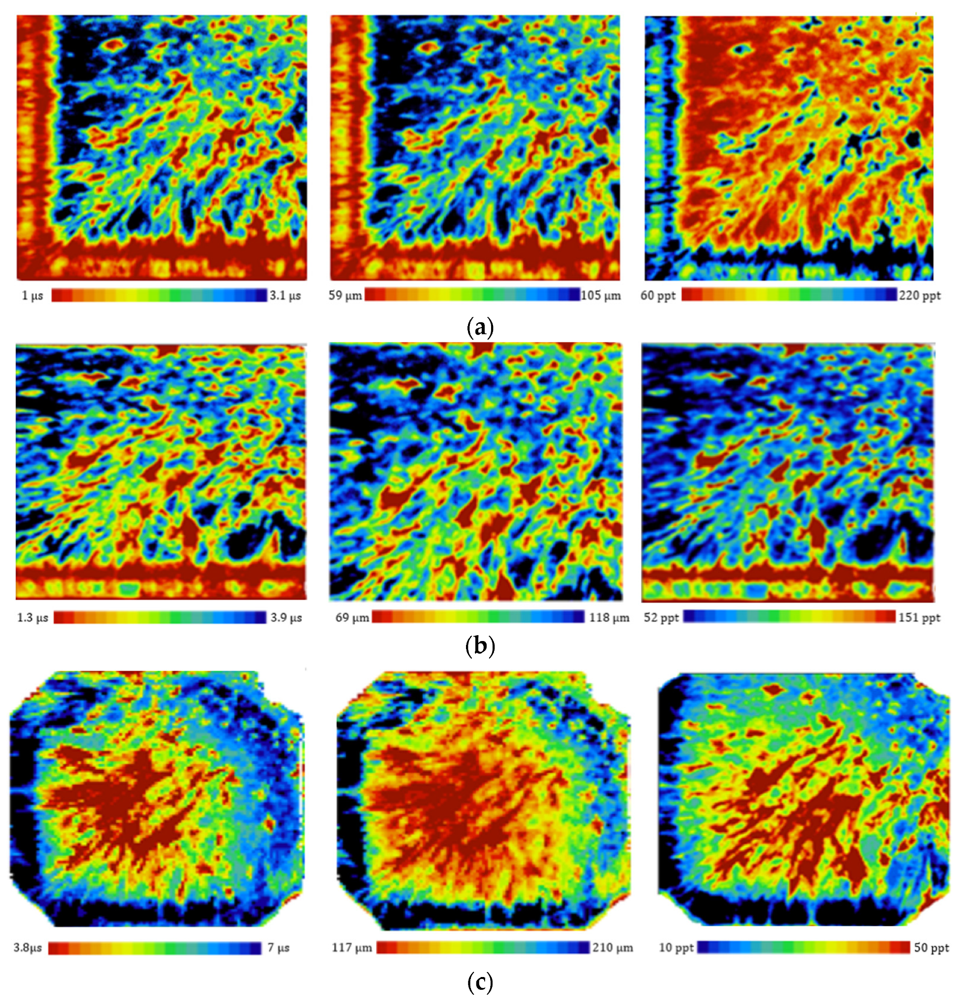
| τeff (µs) | Ldiff (µm) | [Fe] (ppt) | |
|---|---|---|---|
| Bare mc-Si | 1.0–3.1 ± 0.1 | 059–105 ± 5 | 060–220 ± 10 |
| T-mc-Si | 1.3–3.9 ± 0.1 | 069–118 ± 5 | 052–151 ± 10 |
| SiNx/H2 | 3.8–7.0 ± 0.1 | 117–210 ± 5 | 010–050 ± 10 |
Disclaimer/Publisher’s Note: The statements, opinions and data contained in all publications are solely those of the individual author(s) and contributor(s) and not of MDPI and/or the editor(s). MDPI and/or the editor(s) disclaim responsibility for any injury to people or property resulting from any ideas, methods, instructions or products referred to in the content. |
© 2025 by the authors. Licensee MDPI, Basel, Switzerland. This article is an open access article distributed under the terms and conditions of the Creative Commons Attribution (CC BY) license (https://creativecommons.org/licenses/by/4.0/).
Share and Cite
Mannai, A.; Benabderrahmane Zaghouani, R.; Choubani, K.; Almeshaal, M.A.; Rabha, M.B.; Dimassi, W. Electronic Quality Enhancement of Multicrystalline Silicon via SiNx and H2 Plasma Passivation Using Plasma-Enhanced Chemical Vapor Deposition for Photovoltaic Applications. Crystals 2025, 15, 498. https://doi.org/10.3390/cryst15060498
Mannai A, Benabderrahmane Zaghouani R, Choubani K, Almeshaal MA, Rabha MB, Dimassi W. Electronic Quality Enhancement of Multicrystalline Silicon via SiNx and H2 Plasma Passivation Using Plasma-Enhanced Chemical Vapor Deposition for Photovoltaic Applications. Crystals. 2025; 15(6):498. https://doi.org/10.3390/cryst15060498
Chicago/Turabian StyleMannai, Achref, Rabia Benabderrahmane Zaghouani, Karim Choubani, Mohammed A. Almeshaal, Mohamed Ben Rabha, and Wissem Dimassi. 2025. "Electronic Quality Enhancement of Multicrystalline Silicon via SiNx and H2 Plasma Passivation Using Plasma-Enhanced Chemical Vapor Deposition for Photovoltaic Applications" Crystals 15, no. 6: 498. https://doi.org/10.3390/cryst15060498
APA StyleMannai, A., Benabderrahmane Zaghouani, R., Choubani, K., Almeshaal, M. A., Rabha, M. B., & Dimassi, W. (2025). Electronic Quality Enhancement of Multicrystalline Silicon via SiNx and H2 Plasma Passivation Using Plasma-Enhanced Chemical Vapor Deposition for Photovoltaic Applications. Crystals, 15(6), 498. https://doi.org/10.3390/cryst15060498