Article

Numerical Simulation of the Effect of APCVD Reactor Tilted Ceiling Height on Silicon Epitaxial Layer Thickness Uniformity

by
Ba-Phuoc Le
1,
Jyh-Chen Chen
1,*,
Chieh Hu
2,
Wei-Jie Lin
2,
Chun-Chin Tu
2 and
Liang-Chin Chen
2
1
Department of Mechanical Engineering, National Central University, Taoyuan City 320, Taiwan
2
Research and Development Division, Global Wafer Co., Ltd., Hsinchu City 300, Taiwan
*
Author to whom correspondence should be addressed.
Crystals 2025, 15(5), 477; https://doi.org/10.3390/cryst15050477
Submission received: 22 April 2025 / Revised: 10 May 2025 / Accepted: 16 May 2025 / Published: 18 May 2025
(This article belongs to the Section Inorganic Crystalline Materials)

Abstract

As the linewidth of semiconductor nanostructures continues to decrease, the criteria for acceptable surface homogeneity of silicon (Si) epi-films are becoming increasingly stringent. To address this challenge, the effect of different tilted ceiling heights on the Si epi thickness homogeneity in an atmospheric pressure chemical vapor deposition (APCVD) reactor is investigated numerically. In this study, the deposition temperature on the wafer is controlled at 1373 K. When a tilted ceiling with decreasing height along the streamwise direction is used, the average gas mixture velocity increases with the streamwise direction, which can reduce the impact of flow distortion caused by the rotation of the susceptor. At the same time, the growth of the reaction boundary layer on the wafer is suppressed, which helps with the diffusion of trichlorosilane (TCS) on the wafer surface. This makes the drop in the TCS concentration along the streamwise direction more linear, thereby improving the linearity of the growth rate on the wafer surface along the streamwise direction. Therefore, the present results for a reactor without an inlet plate show that the thickness homogeneity across the entire surface of the wafer after a complete susceptor rotation can be significantly improved by linearly reducing the ceiling height in the streamwise direction. A further increase in the inclination of the inclined ceiling leads to a further improvement in the deposition homogeneity. However, the growth rate values at the same position perpendicular to the streamwise direction are inconsistent, which is not conducive to deposition homogeneity. This shortcoming can be improved upon by using a four-inlet plate reactor with an inclined top plate and by properly selecting the position of each partition and the inlet gas mixture velocity of each inlet channel, thereby greatly increasing the deposition homogeneity of the Si epi-layer. For the cases considered in this study, the deposition thickness non-homogeneity across the wafer surface decreased from 38% to 3%.

1. Introduction

Integrated circuits and other microelectronic devices are typically built upon silicon (Si) wafer [1,2,3,4,5,6]. High-purity Si ingots produced via the Czochralski crystal growth technique are commonly used to fabricate these wafers, but still contain very small amounts of oxygen and carbon impurities, as well as crystal defects [7]. In order to meet the requirements of advanced microelectronic devices, and to improve the electrical properties of the wafer, the atmospheric pressure chemical vapor deposition (APCVD) process is usually used to grow a very high purity Si epi-layer on the surface of the Si wafer [8,9,10,11,12,13,14,15,16]. Indeed, the production yield of semiconductor chips is affected by the flatness of this Si epi-layer on the Si wafer. As the nanometer line width further shrinks [17,18,19,20,21,22,23], the surface flatness requirement of this growth layer becomes higher. This becomes the main challenge in growing flatter Si epi-layers during the APCVD process.
There are two main modeling approaches to simulate of epi growth during CVD processes. Atomistic modeling, typically using density functional theory, can provide insights into atomic-scale interactions, surface reactions, and cluster stability, while reactor-scale modeling enables the study of gas flow, thermal distribution, and species transport within the reactor chamber [24,25,26,27]. Reaction modeling is particularly suitable for studying and optimizing the macro-scale design of APCVD systems to improve film thickness homogeneity and deposition efficiency. Various types of APCVD reactors have been utilized to grow the Si epi-layers on Si wafers, including horizontal, vertical, and barrel reactors [28,29,30]. To reduce the production cost of semiconductor manufacturing, large-sized Si wafers are used [31]. Among these reactors, the horizontal APCVD reactor is considered particularly suitable for depositing large-sized wafers, especially 12-inch (300 mm) Si wafers [32,33,34]. In a horizontal APCVD reactor, as the chemical reactions occurring on the wafer surface consume trichlorosilane (TCS), the reaction boundary layer thickness increases along the streamwise direction, leading to a higher growth rate (GR) at the front edge of the wafer than at the rear edge. This results in non-homogeneous deposition of the Si epi-layer on the wafer surface. Wafer rotation is employed to improve the thickness homogeneity by averaging out the higher GR in the front region and the lower GR in the rear region [34]. However, due to the different travel distances of the fluid flow at different wafer front edge positions and the nonlinear distribution of the GR along the streamwise direction caused by the reaction boundary layer, the degree of improvement in the non-homogeneous Si layer deposition caused by susceptor rotation is limited [35]. Le et al. [35] suggested that an ideal GR distribution on the wafer is necessary to achieve perfect thickness homogeneity under susceptor rotation: the GR at the same location perpendicular to the streamwise direction should remain constant, with a linear decrease from the wafer front edge to the rear edge. A common approach to achieve this linear GR reduction from the wafer front edge to the rear edge is to use a higher inlet gas mixture velocity [34,35,36]. This approach also helps minimize the variation in GR difference between the wafer’s front and rear edges. A high inlet gas mixture velocity combined with susceptor rotation can significantly improve deposition homogeneity [34,35,36]. However, the size of the reactor chamber required for the deposition of 12-inch Si wafers is much larger and the gas flow inside the reaction chamber has to travel a longer distance. The Reynolds number (Re) is proportional to the distance traveled by the gas flow and the inlet gas mixture velocity, so it will be larger for larger reaction chamber sizes and higher inlet gas mixture velocities. When Re is higher than a critical value (Rec = 5 × 10 5   for a flat plate flow), the flow pattern changes from a laminar to a transitional flow. In previous studies [3,4,34,35,36,37,38,39], the gas mixture velocity at the inlet has typically ranged from 0.1 m/s to 0.78 m/s, meaning that the order of Re for a 12-inch Si wafer reactor can be as high as O( 10 4 ) . In horizontal APCVD reactors [3,4,5,10,12,34,35,36,37,38,39,40,41,42], the susceptor temperature (973–1500 K) is much higher than the ceiling temperature (400–823 K), so the flow within the reactor might be destabilized by buoyancy [43]. Therefore, the critical Re value might be degraded by buoyancy [43]. Additionally, higher gas mixture velocities at the inlet lead to reactant wastage. To keep the laminar flow inside the reactor and to save on the use of TCS, a low gas inlet velocity is adopted for the deposition of large-size Si wafers. Le et al. [35] found that for small inlet gas mixture velocities, the flow pattern within the reactor is significantly distorted by the susceptor rotation, which also causes non-homogeneity of Si epi-layer deposition. To improve the homogeneity of the Si epi-layer, they proposed using a multi-inlet channel with an appropriate inlet velocity at each inlet to ensure that the instantaneous GR distribution on the wafer is close to the ideal GR distribution [35]. They also showed that the non-homogeneity of Si epi-layer deposition can be further improved by using higher inlet velocities. The average gas flow velocity in the reactor chamber can be enlarged by reducing the cross-sectional area normal to the streamwise direction. The cross-sectional area along the streamwise direction can be decreased by using a sloped ceiling design which suppresses the reaction boundary layer thickness on the wafer surface [44]. Apparently, for small inlet velocities, very highly uniform silicon epi-layer deposition may be achieved by using multiple inlet channels in combination with a sloped ceiling. Therefore, this study used numerical simulation methods to investigate the growth process of silicon epi-layers onto 12-inch (300 mm) silicon wafers in a multi-inlet channel horizontal APCVD with a sloped ceiling. A series of numerical computations was performed to analyze the relationship between the tilted ceiling and the linear GR reduction from the front edge to the rear edge of the wafer. Optimization of the shape of the tilted ceiling and the gas mixture velocities at the inlet to achieve a more uniform Si epi-layer are also discussed.

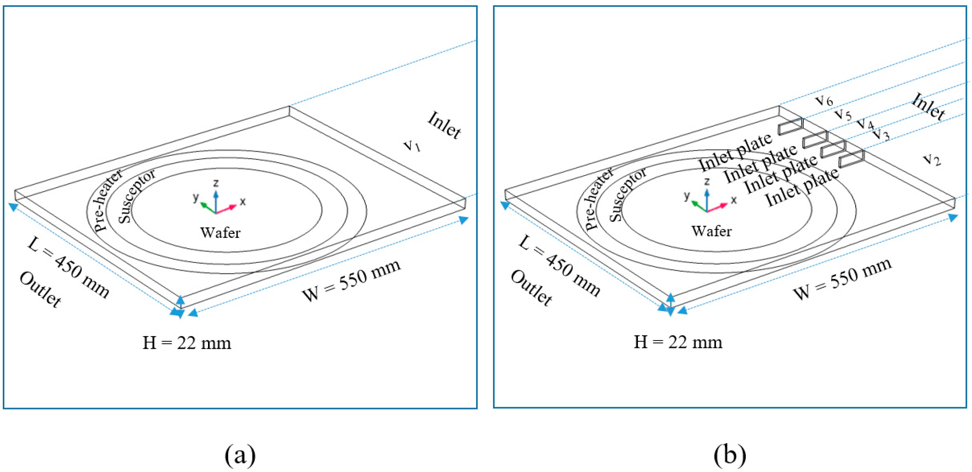
2. Physical System, Governing Equations, and Mathematical Formulation

Figure 1a,b, respectively, show schematic diagrams of the designs used in this study: design 1 (no-inlet plate reactor) and design 2 (four-inlet plate reactor). The ceiling shape is the same. The reactor used in this study was the same as in our previous study [35]. The origin of the coordinate system is fixed at the wafer center and the directions of x, y, and z axes are shown in Figure 1. The reactor dimensions are L = 450 mm × W = 550 mm × H = 22 mm. In our previous study [35], five inlet plates were installed at −95 mm, 0 mm, 47.5 mm, 95 mm, and 161 mm in the y direction. However, it was found that, after optimizing the inlet gas mixture velocity, the velocities on both sides of the inlet plate at −95 mm were the same. Therefore, the inlet plate at −95 mm was removed in this study, and four inlet plates (Figure 1b) were used instead of five inlet plates. The important components were a preheater (radius: 220 mm), a susceptor (radius: 190 mm), and a wafer (radius: 150 mm). Based on our previous study [35,45], the temperatures at the wafer, susceptor, and pre-heater surfaces were chosen to be 1373 K, and the temperature of the reactor wall and gas mixture at the inlet were 823 K and 300 K, respectively. The H2 and TCS gas was well mixed before entering the inlet, and the TCS mass fraction was 0.55. The gas mixture velocity at the inlet of design 1 (v1) was 0.06 m/s. To compare the results obtained between designs 1 and 2 following changes in the height of the outlet, the overall volumetric flow rate entering design 2 was maintained equal to that of design 1. In the case of design 2, there were five channels and, therefore, five velocities at the inlet that should be optimized to improve film thickness homogeneity over the wafer surface. In order to do so, in our previous study [35], the gas mixture velocities at the inlets of the five-inlet plate were adjusted to obtain a constant GR at the same position perpendicular to the streamwise direction. The susceptor was rotated clockwise at 32 rpm. Figure 2 shows schematic diagrams of the APCVD reactor along the xz plane, with and without a change in the outlet height. The height of the ceiling decreased linearly from the position corresponding to the front edge of the wafer to the position corresponding to the rear edge of the wafer. The purpose of this design is to speed up the average velocity of the mixed gas along the streamwise direction, thereby inhibiting the growth of the reaction boundary layer on the wafer, encouraging a linear reduction in the GR on the wafer along the streamwise direction, thereby achieving better thickness homogeneity on the wafer. The reactor height remained constant from the position of the rear edge of the wafer to the outlet. The effect of changing the outlet height was investigated for three cases, including 22 mm, 16 mm, and 10 mm, as shown in Figure 2.

2.1. Governing Equations

The detailed formulation of the governing equations can be found in studies [45,46]. A brief summary is described below:
Mass conservation:
· ρ m U = 0 ,
where ρ m is the gas mixture density, and U is the gas mixture velocity.
Momentum conservation:
ρ m U · U = · p I + μ m U + U T 2 3 μ m · U I + ρ m g ,
where p is the gas mixture pressure, I is the identity tensor, μ m is the mean viscosity of the gas mixture, and g is the gravitational acceleration.
Energy conservation:
· ρ m c p T U = · λ T ,
where cp is the specific heat coefficient of the gas mixture, λ is the thermal conductivity coefficient of the gas mixture, and T is the temperature of the gas mixture.
Conservation of chemical species i (i = SiHCl3, H2 and HCl):
ρ m U · w i = · J i ,
where wi is the mass fraction of chemical species i and J i   is the flux of the diffusive mass transport.
Surface reaction:
For details of the surface reaction, please see Habuka et al. [46]. A summary of the overall reaction and the GR on the wafer is shown below:
Overall reaction on the wafer surface:
SiHCl3 + H2 → Si + 3HCl.
Growth rate:
G R = M s i k o v e r a l l S i H C l 3 [ H 2 ] ρ S i ,
where GR is the growth rate, MSi is the molar mass of Si, koverall is the overall rate constant of Equation (5), [SiHCl3] is the molar concentration of SiHCl3, [H2] is the molar concentration of H2, and ρ S I i is the density of Si.

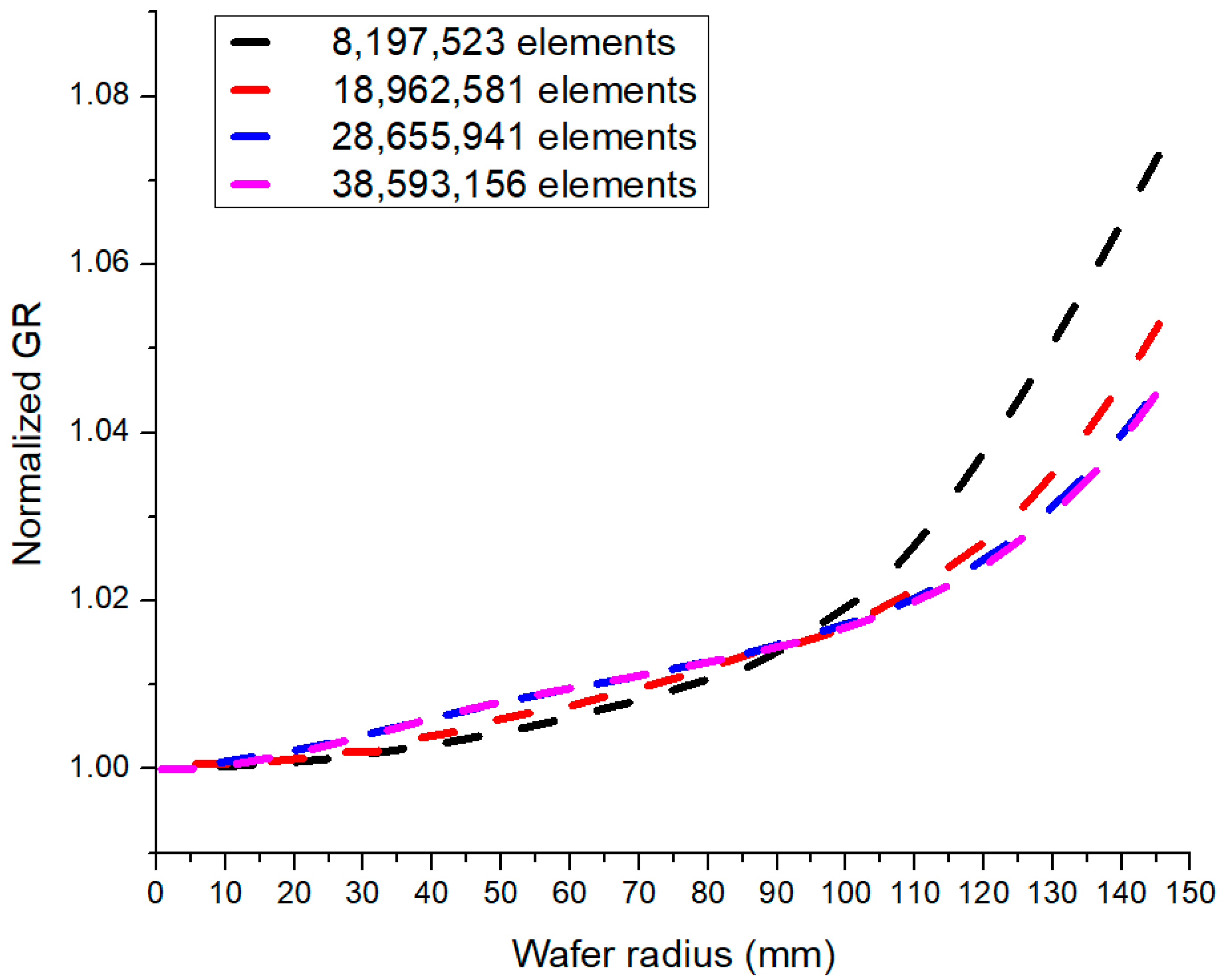
2.2. Numerical Procedure

As in previous studies [35,45,47,48], we used COMSOL Multiphysics software version 6.2 to simulate the fluid dynamics, the heat and mass transfer, and the surface reaction of the CVD process. The study by [45] demonstrated good correlation between the simulation and experimental results for the Si epi APCVD process; therefore, the same approach using COMSOL Multiphysics software version 6.2 was adopted in this study. The governing equations of mass, momentum, energy, and chemical species were solved using the finite element method with linear interpolation functions to estimate the velocity field, pressure distribution, temperature, and species mass fractions. The mesh structure near the wafer surface, the tilted ceiling, and the front and rear edges of the wafer was carefully refined because of rapid changes in the variables. Mesh-independent tests were conducted to evaluate the impact of the resolution of the mesh on the simulation results. The normalized GR for the entire wafer was defined by taking the deposition thickness at each location after a complete rotation, and then dividing this by the deposition thickness at the center of the wafer [35,45]. Examination of the normalized GR under different mesh conditions showed that the normalized GR varied little across the wafer when the number of the mesh elements was higher than 28,655,941 (Figure 3). In addition, when the relative tolerance was set below 0.001, the variation in the GR on the wafer was not obvious. Consequently, the mesh configuration for this study was finalized to have 28,655,941 elements at a relative tolerance of 0.001.

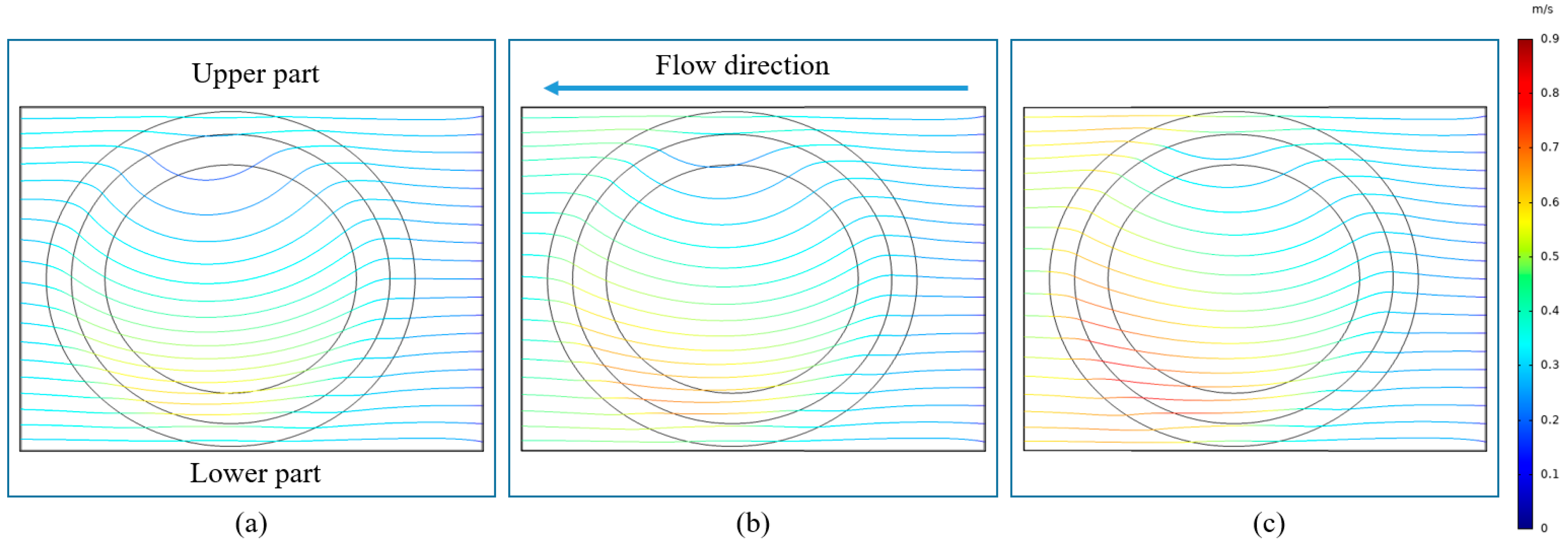
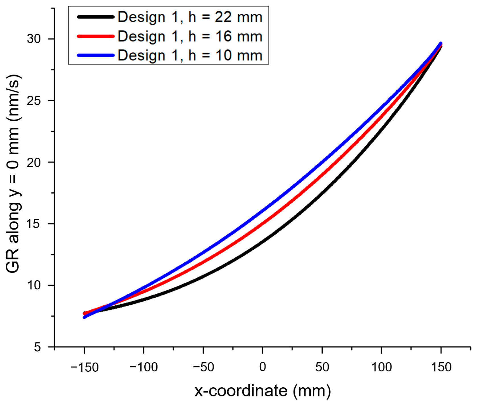
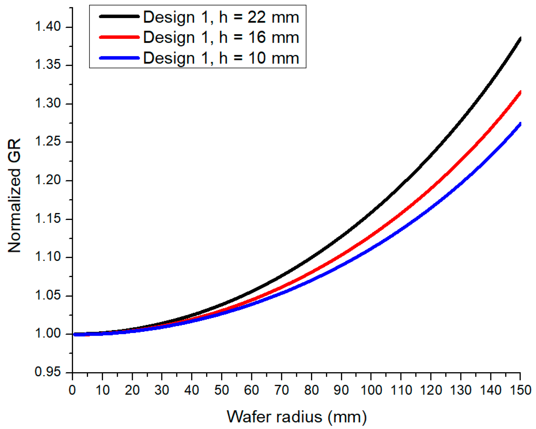
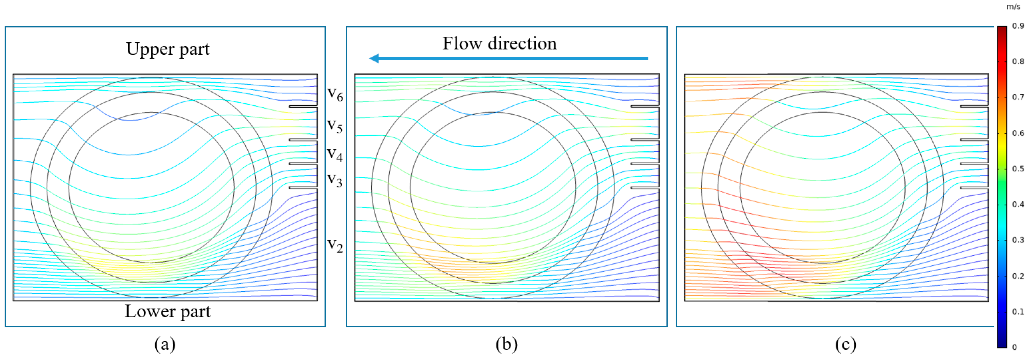
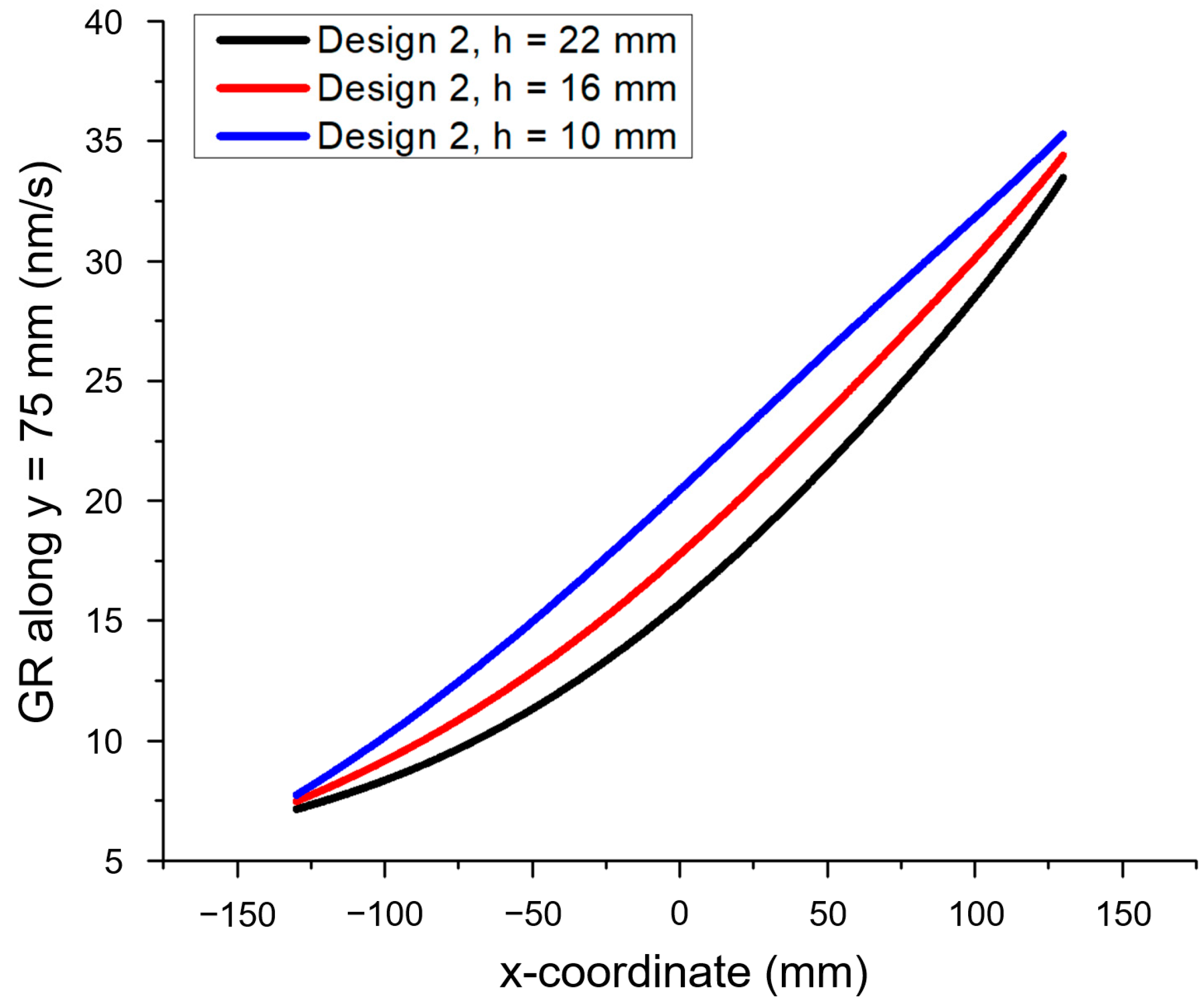
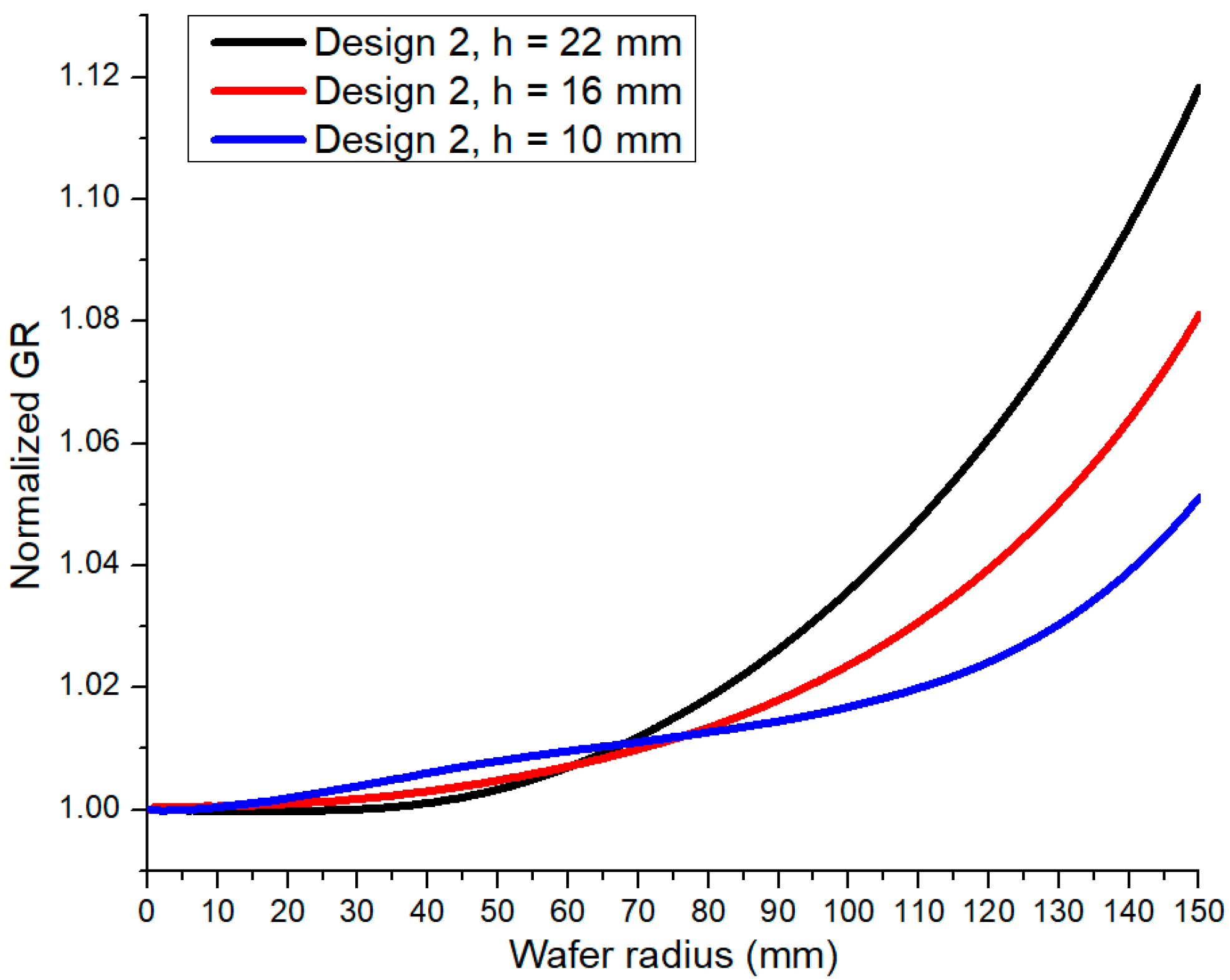
3. Results and Discussion

Figure 4 shows the velocity variation in the xz plane along the streamwise direction through the centerline (y = 0 mm) for design 1 with outlet heights of 22 mm, 16 mm, and 10 mm, and Figure 5 displays the streamlines starting from the inlet at z = 11 mm for these cases. It is obvious that when the outlet height was reduced, the cross-sectional area perpendicular to the streamwise direction decreased, resulting in higher gas mixture velocities. Therefore, the gas mixture velocity from the region at the front edge of the wafer increased along the streamwise direction, as shown in Figure 4. As the susceptor rotated clockwise, streamlines flowed from the inlet to the lower part of the wafer (y < 0 region) and then to the upper part (y > 0 region) (Figure 5). When the height of the outlet was smaller, the influence of the susceptor rotation on the streamlines was smaller because the gas mixture velocity along the streamwise direction was higher. It can be seen that as the outlet height decreased, the streamlines became straighter. Figure 6 and Figure 7 show the TCS concentrations and GR values on the wafer for design 1 with outlet heights of 22 mm, 16 mm, and 10 mm. The TCS was consumed along the streamwise direction at the pre-heater, susceptor, and wafer surface due to surface reactions at high temperature (1373 K). The higher the gas mixture velocity along the streamwise direction, the thinner the reaction boundary layer on the wafer, and the easier it is for TCS to diffuse onto the wafer surface. Since the susceptor rotated clockwise, the gas mixture velocity in the lower part (y < 0 region) along the streamwise direction was higher than the gas mixture velocity in the upper part (y > 0 region) (Figure 5). Therefore, the TCS concentration in the lower part of the wafer (y < 0 region) was higher than that in the upper part (y > 0 region), resulting in a higher GR in the lower part (y < 0 region). It can be seen from Figure 6 and Figure 7 that this effect lessened as the height of the outlet decreased because the effect of the rotation of the susceptor became smaller. Furthermore, the TCS concentration and GR on the wafer appear to be parabolic in shape due to the differences in distance traveled by the gas flow caused by the circular shape of the pre-heater and the wafer. A lower outlet height resulted in higher gas mixture velocity along the streamwise direction, which in turn produced a higher TCS concentration and GR along the streamwise direction on the wafer and reduced the asymmetric effects caused by susceptor rotation (see Figure 6 and Figure 7). Figure 8 shows the GR along the streamwise direction through the centerline (y = 0 mm) of design 1. The GR increased in the streamwise direction as the outlet height decreased due to higher flow velocities. The GR enhancement expanded along the streamwise direction in the front edge region of the wafer. This enhancement was weakened in the rear edge region due to the significant reduction of TCS supply. However, the TCS toward the rear edge of the wafer (x = −150 mm) was still insufficient, so there was no increase with a decreasing outlet height. Therefore, there was no significant difference in the GR at the rear edge of the wafer for outlet heights of 22, 16, and 10 mm. Hence, the GR decreased more linearly from the front edge to the rear edge of the wafer. Figure 9 shows the normalized GR obtained for design 1 using different outlet heights. When the outlet height was reduced, there was a significant improvement in the linear reduction in the GR along the streamwise direction, which improved the thickness homogeneity across the wafer, as shown in Figure 9.
From the results shown in Figure 7, it can be observed that the GR at locations perpendicular to the streamwise direction (GR at the same x-coordinates) were not close to the same values. Our previous study [35] showed that the use of a multi-inlet plate reactor with appropriate flow speeds in different flow channels can make the GR distribution on the wafer approach a constant value perpendicular to the streamwise direction. Therefore, combining a sloped ceiling with a multi-inlet plate design may bring the GR distribution closer to the ideal, further improving the thickness homogeneity on the wafer. A schematic diagram of the reactor is shown in Figure 1b. The gas inlet velocities v2, v3, v4, v5, and v6 of design 2, which produced good deposition homogeneity, were 0.01 m/s, 0.1 m/s, 0.12 m/s, 0.23 m/s, and 0.01 m/s, respectively [35]. These were the velocities used in this study. The streamlines starting from the inlets of design 2 are shown in Figure 10. In these cases, the streamlines were also affected by the clockwise rotation of the susceptor. The streamlines starting for inlet velocities v3 and v4 covered the lower part of the wafer (y < 0 region), while the streamlines for inlet velocity v5 covered the upper part of the wafer (y > 0 region). When the outlet height was lower, the gas mixture velocity along the streamwise direction was higher (Figure 10), so the effect of clockwise rotation on the streamlines was reduced. The TCS concentrations and GR on the wafer surface from design 2 with different outlet heights are shown in Figure 11 and Figure 12. When the outlet height was 22 mm, the results were the same as the best case considered in our previous study [35], that is, except at the rear edge of the wafer, the GR was closer to a constant value at the same x-coordinate. It is worth pointing out that the v5 inlet provided more TCS than the v4 and v3 inlets (v5 = 0.23 m/s > v4 = 0.12 m/s > v3 = 0.1 m/s). When the flow velocity was higher, the rotational effect of the susceptor was weaker, in which case, more TCS was carried to the upper part of the wafer (y > 0 region) due to the enhanced flow velocity caused by the reduced outlet height. Hence, the enhancement of the TCS concentration and GR was more significant in the upper part (y > 0 region) than in the lower part (y < 0 region). Figure 13, Figure 14 and Figure 15 show the GR on the wafer along the streamwise direction at y = 75 mm, 0 mm, and −75 mm, respectively, for three different outlet heights. It is clear that the linear GR reduction at three y positions along the streamwise direction improved with decreasing outlet height. Figure 16 shows the normalized GR on the wafer for design 2 obtained with outlet heights of 22, 16, and 10 mm. In general, as the outlet height decreased from 22 mm to 10 mm, the overall thickness non-homogeneity was significantly reduced due to the improved linear reduction in the GR along the streamwise direction. However, on the wafer with a radius of less than 70 mm, there was a slight deterioration in the thickness homogeneity as the outlet height decreased.
It can be seen from Figure 11 that, as the outlet height decreased, the unevenness of the TCS concentration in the upper (y > 0 region) and lower parts of the wafer (y < 0 region) near the front edge became more obvious. Consequently, the GR at the same x-coordinate became less consistent (Figure 12) in this region as the outlet height decreased. In order to further enhance the homogeneity of the deposited layer, the inlet gas mixture velocities of design 2 with an outlet height of 10 mm needed to be further adjusted to achieve a more consistent GR at the same x-coordinate. According to our previous research results [35], inlet gas mixture velocity v5 should be reduced to decrease the TCS concentration in the upper region of the wafer (y > 0 region), while inlet gas mixture velocities v3 and v4 should be increased to enhance the TCS concentration in the lower region of the wafer (y < 0 region). The optimized values for an outlet height of 10 mm, while keeping the total inlet volume flow rate the same as in the previous cases, were v2 = 0.01 m/s, v3 = 0.139 m/s, v4 = 0.153 m/s, v5 = 0.18 m/s, and v6 = 0.01 m/s. In this case, the differences among inlet gas mixture velocities v3, v4, and v5 were smaller than with the previous design 2. This reduction in the velocity difference was beneficial to flow stability inside the reactor, as larger velocity differences between adjacent flows may lead to the formation of local vortices and thus to inhomogeneous deposition. Figure 17 shows the streamlines starting from the inlet, the TCS concentration on the wafer, and the GR on the wafer for the optimized case of design 2 with an outlet height of 10 mm. By comparing Figure 17a with Figure 10c, it can be seen that in this new case, since the inlet velocity of v5 was smaller, the region of streamline influence was smaller. On the other hand, the increase in the velocities of v3 and v4 affected a larger streamline region. The lower inlet velocity of v5 resulted in lower TCS concentrations and GR in the upper part of the wafer (y > 0 region), while the higher inlet velocities of v3 and v4 resulted in higher TCS concentrations and GR in the lower part of the wafer (y < 0 region) (Figure 11c and Figure 17b; Figure 12c and Figure 17c). The decrease in the inlet gas mixture velocity of v5 and the increase in the inlet gas mixture velocities of v3 and v4 drove the GR at the same x-coordinate in the front edge closer to a consistent value. As can be seen in Figure 18, an enhancement in the thickness homogeneity on the wafer was achieved with a reduction in the velocity of v5 and increasing velocities of v3 and v4.

4. Conclusions

This study investigated the effect of a tilted ceiling on the homogeneity of the Si epi-layer deposited on an Si wafer. The chemical reactions, flow dynamics, and heat and mass transport in a simplified APCVD reactor were simulated. When an inclined top plate with decreasing height in the streamwise direction was used, the cross-sectional area of the flow channel decreased along the streamwise direction. Therefore, the average gas flow velocity increased, which reduced the impact of gas flow distortion caused by the rotation of the susceptor. On the other hand, when the gas mixture velocity along the streamwise direction was higher, the growth of the reactive boundary layer on the wafer was suppressed, which helped the diffusion of TCS on the wafer surface. This led to a linear decrease in the TCS concentration along the streamwise direction, thereby improving the linearity of the GR on the wafer surface along the streamwise direction. Hence, the present results for a no-inlet plate reactor (design 1) show that the thickness homogeneity on the wafer can be significantly improved using a tilted top ceiling where the height decreases along the streamwise direction. An increase in the inclination of the inclined top plate further enhanced the deposition homogeneity. However, in the case of design 1, the GR values at the same location perpendicular to the streamwise direction were highly inconsistent. Therefore, a four-inlet plate reactor design (design 2) with a tilted ceiling was adopted to further improve the thickness homogeneity across the wafer. Under the same total volume flow rate conditions, more consistent GR values at the same x-coordinate were achieved by properly selecting the inlet gas mixture velocity for each inlet channel, further improving the homogeneity of the deposition. For design 1, under the conditions considered in this study, a linear reduction in the height of the reactor ceiling from 22 mm to 10 mm led to an improvement in the non-homogeneity of deposition thickness on the wafer from 38% to 28%, compared with the case where the ceiling height remains unchanged. The selection of the appropriate plate inlet positions and gas mixture velocity for each channel in design 2 can reduce the wafer thickness non-homogeneity to 3%, with a linear reduction in the ceiling height from 22 mm to 10 mm.

Author Contributions

Conceptualization: C.H., C.-C.T. and L.-C.C.; data curation: C.H. and C.-C.T.; formal analysis: B.-P.L. and W.-J.L.; funding acquisition: J.-C.C.; investigation: B.-P.L.; methodology: B.-P.L., J.-C.C. and W.-J.L.; project administration: J.-C.C. and L.-C.C.; resources, C.H. and C.-C.T.; software: B.-P.L. and W.-J.L.; supervision: J.-C.C.; writing—original draft: B.-P.L.; writing—review and editing: J.-C.C. All authors have read and agreed to the published version of the manuscript.

Funding

This research received no external funding.

Data Availability Statement

The original contributions presented in this study are included in the article. Further inquiries can be directed to the corresponding author.

Conflicts of Interest

Authors Chieh Hu, Wei-Jie Lin, Chun-Chin Tu and Liang-Chin Chen were employed by the company Global Wafer Co., Ltd. The remaining authors declare that the research was conducted in the absence of any commercial or financial relationships that could be construed as a potential conflict of interest.

References

  1. Kim, T.; Lee, J. Fabrication and characterization of silicon-on-insulator wafers. Micro Nano Syst. Lett. 2023, 11, 15. [Google Scholar] [CrossRef]
  2. Hossain, N.; Mahmud, M.Z.A.; Hossain, A.; Rahman, M.K.; Islam, M.S.; Tasnim, R.; Mobarak, M.H. Advances of materials science in MEMS applications: A review. Results Eng. 2024, 22, 102115. [Google Scholar] [CrossRef]
  3. Habuka, H.; Katayama, M.; Shimada, M.; Okuyama, K. Nonlinear increase in silicon epitaxial growth rate in a SiHCl3-H2 system under atmospheric pressure. J. Cryst. Growth 1997, 182, 352–362. [Google Scholar] [CrossRef]
  4. Habuka, H.; Fukaya, S.; Sawada, A.; Takeuchi, T.; Aihara, M. Flatness deterioration of silicon epitaxial film formed in a horizontal single-wafer epitaxial reactor II. Jpn. J. Appl. Phys. 2002, 41, 5692–5696. [Google Scholar] [CrossRef]
  5. Faller, F.R.; Hurrle, A. High-temperature CVD for crystalline-silicon thin-film solar cells. IEEE Trans. Electron Devices 1999, 46, 2048–2054. [Google Scholar] [CrossRef]
  6. Shimura, F. Semiconductor Silicon Crystal Technology, 1st ed.; Harcourt Brace Jovanovich: San Diego, CA, USA, 1989. [Google Scholar]
  7. Tilli, M.; Krockel, M.P.; Petzold, M.; Theuss, H.; Motooka, T.; Lindroos, V. Handbook of Silicon Based MEMS Materials and Technologies, 3rd ed.; Matthew Deans: London, UK, 2020. [Google Scholar]
  8. Li, C.; Li, C.; Jiang, H.; Chen, H.; Fang, H. Analysis of influencing factors on silicon epitaxial growth in horizontal single-wafer reactor through orthogonal test. Cryst. Res. Technol. 2024, 59, 2300237. [Google Scholar] [CrossRef]
  9. Ramadan, Z.; Im, I.T.; Park, C.W. Process optimization and modeling of the silicon growth in trichlorosilane-hydrogen gas mixture in a planetary CVD reactor. IEEE Trans. Semicond. Manuf. 2021, 34, 1–8. [Google Scholar] [CrossRef]
  10. Habuka, H.; Aoyama, Y.; Akiyama, S.; Otsuka, T.; Qu, W.F.; Shimada, M.; Okuayama, K. Chemical process of silicon epitaxial growth in a SiHCl3-H2 system. J. Cryst. Growth 1999, 207, 77–86. [Google Scholar] [CrossRef]
  11. Saito, A.; Miyazaki, K.; Matsui, M.; Habuka, H. In-situ observation of chemical vapor deposition using SiHCl3 nad BCl3 gases. Phys. Status Solidi 2015, 12, 953–957. [Google Scholar]
  12. Jeon, S.; Park, H.; Oh, H.J.; Kim, W.K. Computational modeling of a chemical vapor deposition reactor for epitaxial silicon formation. Sci. Adv. Mater. 2016, 8, 578–582. [Google Scholar] [CrossRef]
  13. Makino, S.; Inagaki, M.; Nakashima, K.; Kozawa, T.; Horinouchi, N. A simplified reaction reaction model and numerical analysis for Si depositon from SiHCl3-H2 system in vertical rotating disk reactors. J. Cryst. Growth 2016, 454, 156–163. [Google Scholar] [CrossRef]
  14. Miyazaki, K.; Saito, A.; Habuka, H. In situ measurement for evaluating temperature change related to silicon film formation in a SiHCl3-H2 system. ECS J. Solid State Sci. Technol. 2015, 5, 16–20. [Google Scholar] [CrossRef]
  15. Koosha, N.; Sabet, J.K.; Moosavian, M.A.; Amini, Y. Improvement of synthesized graphene structure through various solvent liquids at low temperatures by chemical vapor deposition method. Mater. Sci. Eng. B 2021, 274, 115458. [Google Scholar] [CrossRef]
  16. Saito, A.; Sakurai, A.; Habuka, H. Increase in silicon film deposition rate in SiHCl3-SiHx-H2 system. J. Cryst. Growth 2017, 468, 204–207. [Google Scholar] [CrossRef]
  17. Lundstrom, M.S.; Lam, M.A. Moore’s law: The journey ahead. Science 2022, 378, 722–723. [Google Scholar] [CrossRef]
  18. Jeong, J.; Lee, S.H.; Masuoka, S.A.; Min, S.; Lee, S.; Kim, S.; Myung, T.; Choi, B.; Sohn, C.W.; Kim, S.W.; et al. World’s first GAA 3nm foundry platform technology (SF3) with novel multi-bridge-channel-FET (MBCFETTM) Process. In Proceedings of the 2023 IEEE Symposium on VLSI Technology and Circuits (VLSI Technology and Circuits), Kyoto, Japan, 11–16 June 2023; pp. 1–2. [Google Scholar]
  19. Kao, I.; Chung, C. Wafer Manufacturing: Shaping of Single Crystal Silicon Wafers, 1st ed.; Wiley: Hoboken, NJ, USA, 2021. [Google Scholar]
  20. Kunle, M.; Baumgartl, J.; Ackermann, T. Uniformity improvement for 200mm APCVD epitaxial Si film by retrofit of applied materials epi centura. In Proceedings of the SEMI Advanced Semiconductor Manufacturing Conference, Saratoga Springs, NY, USA, 19–21 May 2014; Volume 25, pp. 389–392. [Google Scholar]
  21. Levinson, H.J. High-NA EUV lithography: Current status and outlook for the future. Jpn. J. Appl. Phys. 2022, 61, SD0803-1–SD0803-18. [Google Scholar] [CrossRef]
  22. Irikura, K.; Muroi, M.; Yamada, A.; Matsuo, M.; Habuka, H.; Ishida, Y.; Ikeda, S.I.; Hara, S. Advantages of a slim vertical gas channel at high SiHCl3 concentrations for atmospheric pressure silicon epitaxial growth. Mater. Sci. Semicond. Process. 2018, 87, 13–18. [Google Scholar] [CrossRef]
  23. Lee, H.; Lee, J.; Kim, S.; Lee, C.; Han, S.; Kim, M.; Kwon, W.; Park, S.K.; Veeraraghavan, S.; Kim, J.; et al. Improvement of depth of focus control using wafer geometry. SPIE Adv. Lithogr. 2015, 9424, 942428-1–942428-6. [Google Scholar]
  24. Pacheco, J.M.; Gueorguiev, G.K.; Martins, J.L. First-principles study of the possibility of condensed phases of endohedral silicon cage clusters. Phys. Rev. B 2002, 66, 033401. [Google Scholar] [CrossRef]
  25. Gueorguiev, G.K.; Stafstrom, S.; Hultman, L. Nano-wire formation by self-assembly of silicon-metal cage-like molecules. Chem. Phys. Lett. 2008, 458, 170–174. [Google Scholar] [CrossRef]
  26. Sibanda, D.; Oyinbo, S.T.; Jen, T.C. A review of atomic layer deposion modelling and simulation methodologies: Density functional theory and molecular dynamics. Nanotechnol. Rev. 2022, 11, 1332–1363. [Google Scholar] [CrossRef]
  27. Tian, Y.; Yan, Z.; Jiang, L.; Liu, R.; Liu, B.; Shao, Y.; Yang, X.; Lu, M. Multiscale models of CVD process: Review and prospective. Materials 2024, 17, 5131. [Google Scholar] [CrossRef]
  28. Holstein, W.L. Design and modeling of chemical vapor deposition reactors. Prog. Cryst. Growth Charact. Mater. 1992, 24, 111–211. [Google Scholar] [CrossRef]
  29. Fischer, A.; Kissinger, G.; Ritter, G.; Akhmetov, V.; Kittler, M. Plastic deformation in 200 mm silicon wafers arising from mechanical loads in vertical-type and horizontal-type furnaces. Mater. Sci. Eng. B 2009, 159–160, 103–106. [Google Scholar] [CrossRef]
  30. Sivaram, S. Chemical Vapor Deposition: Thermal and Plasma Deposition of Electronic Materials; Van Nostrand Reinhold: New York, NY, USA, 1995. [Google Scholar]
  31. Hahn, P.O. The 300 mm silicon wafer—A cost and technology challenge. Microelectron. Eng. 2001, 56, 3–13. [Google Scholar] [CrossRef]
  32. Deng, B.; Liu, Z.; Peng, H. Toward mass production of CVD graphene films. Adv. Mater. 2018, 31, 1800996. [Google Scholar] [CrossRef]
  33. Rinaldi, A.M.; Crippa, D. Chapter 1 CVD teachnologies for silicon: A quick survey. Semicond. Semimet. 2001, 72, 1–50. [Google Scholar]
  34. Kommu, S.; Wilson, G.M.; Khomami, B. A theoretical/experimental study of silicon epitaxy in horizontal single-wafer chemical vapor deposition reactors. J. Electrochem. Soc. 2000, 147, 1538–1550. [Google Scholar] [CrossRef]
  35. Le, B.P.; Chen, J.C.; Hu, C.; Lin, W.J.; Tu, C.C.; Chen, L.C. Numerical analysis of the use of multiple inlet plates to improve the thickness uniformity of silicon epitaxial layers during atmospheric pressure chemical vapor deposition. Results Eng. 2024, 24, 103688. [Google Scholar] [CrossRef]
  36. Kommu, S.; Khomami, B. High-volume single-wafer reactors for silicon epitaxy. Ind. Eng. Chem. Res. 2002, 41, 732–743. [Google Scholar] [CrossRef]
  37. Salinger, A.G.; Pawlowski, R.P.; Shadid, J.N.; Waanders, B.G.V.B. Computational analysis and optimization of a chemical vapor deposition reactor with large-scale computing. Ind. Eng. Chem. Res. 2004, 43, 4612–4623. [Google Scholar] [CrossRef]
  38. Habuka, H. Flatness deterioration of Silicon epitaxxial film formed using horizontal single-wafer epitaxial reactor. Jpn. J. Appl. Phys. 2001, 40, 6041–6044. [Google Scholar] [CrossRef]
  39. Habuka, H.; Fukaya, S.I.; Sawada, A.; Takeuchi, T.; Aihara, M. Formation mechanism of local thickness profile of silicon epitaxial film. J. Cryst. Growth 2004, 266, 327–332. [Google Scholar] [CrossRef]
  40. Fang, M.; Xiong, Y.Y.; Yuan, X.Z.; Liu, Y.W. Numerical analysis of the chemical vapor deposition of polysilicon in a trichlorosilane and hydrogen system. Energy Procedia 2014, 61, 1987–1991. [Google Scholar] [CrossRef]
  41. Habuka, H.; Katayama, M.; Shimada, M.; Okuyama, K. Numerical evaluation of Silicon-thin film growth from SiHCl3-H2 gas mixture in a horizontal vapor deposition reactor. Jpn. J. Appl. Phys. 1994, 33, 1977–1985. [Google Scholar] [CrossRef]
  42. Angermeier, D.; Monna, R.; Slaoui, A.; Muller, J.C. Modeling and analysis of the Silicon epitaxial growth with SiHCl3 in a horizontal rapid thermal chemical vapor deposiiton reactor. J. Electrochem. Soc. 1997, 144, 3256–3261. [Google Scholar] [CrossRef]
  43. Garbrecht, O. Large Eddy Simulation of Three-Dimentional Mixed Convection on a Vertical Plate. Ph.D. Thesis, RWTH Aachen University, Aachen, Germany, 2017. [Google Scholar]
  44. Cheng, T.S.; Hsiao, M.C. Numerical investigations of geometric effects on flow and thermal fields in a horizontal CVD reactor. J. Cryst. Growth 2008, 310, 3097–3106. [Google Scholar] [CrossRef]
  45. Le, B.P.; Lin, W.J.; Chen, J.C.; Hu, C.; Tu, C.C.; Chen, L.C. Numerical and experimental investigation of the effect of side injectors on the deposition rate near the wafer edge during atmospheric pressure chemical vapor deposition. Mater. Sci. Semicond. Process. 2024, 172, 108085. [Google Scholar] [CrossRef]
  46. Habuka, H.; Nagoya, T.; Mayusumi, M.; Katayama, M.; Shimada, M.; Okuyama, K. Model on transport phenomena and epitaxial growth of silicon thin film in SiHCl3-H2 system under atmospheric pressure. J. Cryst. Growth 1996, 169, 61–72. [Google Scholar] [CrossRef]
  47. Lin, W.J.; Chen, J.C. A numerical study of the effect of pulse duration on preventing particle generation during the AlN pulsed MOCVD process. Mater. Sci. Semicond. Process. 2022, 148, 106816. [Google Scholar] [CrossRef]
  48. Lin, W.J.; Chen, J.C. Numerical Study of Growth Rate and Purge Time in the AlN Pulsed MOCVD Process. Crystals 2022, 12, 1101. [Google Scholar] [CrossRef]
Figure 1. Schematic diagrams of the reactor without changing the outlet height for the (a) no-inlet plate reactor (design 1) and (b) the four-inlet plate reactor (design 2).
Crystals 15 00477 g001
Figure 2. Schematic diagrams of the APCVD reactor (xz plane view) with three outlet heights: h = 22 mm, h = 16 mm, and h = 10 mm.
Crystals 15 00477 g002
Figure 3. Mesh-independent test results for design 2 with an outlet height of 10 mm at v2 = 0.01 m/s, v3 = 0.1 m/s, v4 = 0.12 m/s, v5 = 0.23 m/s, and v6 = 0.01 m/s.
Crystals 15 00477 g003
Figure 4. Velocity distribution at v1 = 0.06 m/s in the xz plane along the streamwise direction through the centerline (y = 0 mm) for design 1 with outlet heights of 22 mm, 16 mm, and 10 mm, respectively.
Crystals 15 00477 g004
Figure 5. Streamlines starting from the inlet of design 1 at z = 11 mm with v1 = 0.06 m/s: (a) without changing the outlet height, h = 22 mm; (b) with changing the outlet height, h = 16 mm, and (c) with changing the outlet height, h = 10 mm. The color of the streamlines represents the velocity magnitude.
Crystals 15 00477 g005
Figure 6. TCS concentration on the wafer surface (xy plane at z = 0 mm) at v1 = 0.06 m/s for design 1: (a) without changing the outlet height, h = 22 mm; (b) with changing the outlet height, h = 16 mm, and (c) with changing the outlet height, h = 10 mm.
Crystals 15 00477 g006
Figure 7. GR on the wafer surface (xy plane at z = 0 mm) at v1 = 0.06 m/s for design 1: (a) without changing the outlet height, h = 22 mm; (b) with changing the outlet height, h = 16 mm, and (c) with changing the outlet height, h = 10 mm.
Crystals 15 00477 g007
Figure 8. GR at v1 = 0.06 m/s along the streamwise direction through the centerline (y = 0 mm) for design 1 with outlet heights of 22 mm, 16 mm, and 10 mm.
Crystals 15 00477 g008
Figure 9. Normalized GR at v1 = 0.06 m/s for design 1, with outlet heights of 22 mm, 16 mm, and 10 mm.
Crystals 15 00477 g009
Figure 10. Streamlines starting from the inlet of design 2 at z = 11 mm with v2 = 0.01 m/s, v3 = 0.1 m/s, v4 = 0.12 m/s, v5 = 0.23 m/s, and v6 = 0.01 m/s: (a) without changing the outlet height, h = 22 mm; (b) with changing the outlet height, h = 16 mm, and (c) with changing the outlet height, h = 10 mm.
Crystals 15 00477 g010
Figure 11. TCS concentration on the wafer surface (xy plane at z = 0 mm) at v2 = 0.01 m/s, v3 = 0.1 m/s, v4 = 0.12 m/s, v5 = 0.23 m/s, v6 = 0.01 m/s for design 2: (a) without changing the outlet height, h = 22 mm; (b) with changing the outlet height, h = 16 mm, and (c) with changing the outlet height, h = 10 mm.
Crystals 15 00477 g011
Figure 12. GR distribution on the wafer surface (xy plane at z = 0 mm) at v2 = 0.01 m/s, v3 = 0.1 m/s, v4 = 0.12 m/s, v5 = 0.23 m/s, v6 = 0.01 m/s for design 2: (a) without changing the outlet height, h = 22 mm; (b) with changing the outlet height, h = 16 mm and (c) with changing the outlet height, h = 10 mm.
Crystals 15 00477 g012
Figure 13. The GR along y = 75 mm at v2 = 0.01 m/s, v3 = 0.1 m/s, v4 = 0.12 m/s, v5 = 0.23 m/s, and v6 = 0.01 m/s for design 2 with outlet heights of 22 mm, 16 mm, and 10 mm.
Crystals 15 00477 g013
Figure 14. GR along y = 0 mm at v2 = 0.01 m/s, v3 = 0.1 m/s, v4 = 0.12 m/s, v5 = 0.23 m/s, and v6 = 0.01 m/s for design 2 with outlet heights of 22 mm, 16 mm, and 10 mm.
Crystals 15 00477 g014
Figure 15. GR along y = −75 mm at v2 = 0.01 m/s, v3 = 0.1 m/s, v4 = 0.12 m/s, v5 = 0.23 m/s, and v6 = 0.01 m/s for design 2 with outlet heights of 22 mm, 16 mm, and 10 mm.
Crystals 15 00477 g015
Figure 16. Normalized GR at v2 = 0.01 m/s, v3 = 0.1 m/s, v4 = 0.12 m/s, v5 = 0.23 m/s, and v6 = 0.01 m/s for design 2 with outlet heights of 22 mm, 16 mm, and 10 mm.
Crystals 15 00477 g016
Figure 17. Design 2 with an outlet height of 10 mm for v2 = 0.01 m/s, v3 = 0.139 m/s, v4 = 0.153 m/s, v5 = 0.18 m/s, and v6 = 0.01 m/s: (a) streamlines starting from the inlet at z = 11 mm, (b) TCS concentration at the wafer surface (xy plane z = 0 mm), and (c) GR at the wafer surface (xy plane z = 0 mm).
Crystals 15 00477 g017
Figure 18. Normalized GR for design 2 with an outlet height of 10 mm and various inlet velocities (v2, v3, v4, v5, v6) = (0.01, 0.1, 0.12, 0.23, 0.01) m/s and (0.01, 0.139, 0.153, 0.18, 0.01) m/s.
Crystals 15 00477 g018
Disclaimer/Publisher’s Note: The statements, opinions and data contained in all publications are solely those of the individual author(s) and contributor(s) and not of MDPI and/or the editor(s). MDPI and/or the editor(s) disclaim responsibility for any injury to people or property resulting from any ideas, methods, instructions or products referred to in the content.

