Article

Anisotropy of Voltage Sensitivity of Bow-Tie Microwave Diodes Containing 2DEG Layer

by
Algirdas Sužiedėlis
1,*,
Steponas Ašmontas
1,
Jonas Gradauskas
1,2,
Aurimas Čerškus
1,3,
Andžej Lučun
1,
Maksimas Anbinderis
1,4 and
Ihor Zharchenko
1
1
Center for Physical Sciences and Technology, Saulėtekio Ave. 3, LT-10257 Vilnius, Lithuania
2
Department of Physics, Vilnius Gediminas Technical University, Saulėtekio Ave. 11, LT-10223 Vilnius, Lithuania
3
Department of Mechatronics, Robotics and Digital Manufacturing, Vilnius Gediminas Technical University, Plytinės st. 25, LT-10105 Vilnius, Lithuania
4
Department of Electrical Engineering, Vilnius Gediminas Technical University, Saulėtekio Ave. 11, LT-10223 Vilnius, Lithuania
*
Author to whom correspondence should be addressed.
Crystals 2025, 15(4), 367; https://doi.org/10.3390/cryst15040367
Submission received: 7 March 2025 / Revised: 1 April 2025 / Accepted: 14 April 2025 / Published: 17 April 2025

Abstract

:
Microwave Bow-Tie Diodes operate across a broad frequency range, including THz radiation detection and THz imaging applications. When fabricated using modulation-doped structures, these diodes exhibit enhanced detection properties that are best characterized by voltage sensitivity. The sensitivity is influenced by multiple factors, including diode design, semiconductor material quality, and the characteristics of the ohmic contacts. In this study, we examine how the electrical properties of modulation-doped bow-tie diodes are affected by their orientation relative to the crystallographic axes. Extensive investigations on various bow-tie diodes exposed to broadband microwave radiation, both in darkness and under white and infrared light illumination, enabled us to identify the optimal diode designs and illumination conditions for maximizing sensitivity to electromagnetic radiation. Based on our findings, we provide recommendations for diode design and illumination conditions to enhance the diode’s sensitivity to microwave radiation while minimizing illumination-induced effects on electrical properties.

1. Introduction

The concept of anisotropy appears in various aspects of everyday life, ranging from the macro- to the micro-world. In physics, anisotropy is most prominent in monocrystalline materials, where the mechanical, optical, thermal, and electrical properties of a material vary depending on the crystallographic direction. Electrical anisotropy is usually not encountered in the case of weak electric fields; however, the anisotropy of an electrical current can be observed in cubic semiconductors when the charge carriers are heated by a strong electric field. The anisotropic electrical properties of the many-valley cubic semiconductors result from the repopulation of different valleys by electrons or from the difference in the effective masses of holes along different crystallographic directions. In cubic covalent semiconductors such as Ge and Si, the anisotropy of the hot electron drift velocity and diffusion coefficients has been determined by the repopulation of different energy valleys and the non-parabolicity of the lowest valleys of Ge [1]. In the case of cubic polar semiconductors, such as GaAs, a slight anisotropy of electron drift velocity has been declared to date [1]. The conductivity anisotropy in n-GaAs was first observed experimentally at liquid nitrogen temperature, and this effect was explained by the different distributions of electrons among the satellite energy minima [2]. The same authors developed a theoretical method enabling the definition of strong-field conduction anisotropies in many-valley cubic semiconductors [3]. They stated that the conditions for the conduction of anisotropy to appear were determined by the location and shape of the energy surfaces. At that time, data were available only for Ge and Si, and the comparisons between the experimentally determined longitudinal anisotropy parameters and the calculated values were presented for these materials. The calculated longitudinal anisotropy in n-GaAs was also presented; however, it was close to unity [3]. A large anisotropy of the electron g-factor in a GaAs/AlGaAs quantum well (QW) structure was reported in ref. [4]. The dependence of the hole effective mass on the crystallographic direction was observed in the GaAs-(Ga,Al)As two-dimensional hole systems [5]. An extremely large conductance anisotropy was observed in the MBE-grown n-AlGaAs/GaAs heterojunction on a vicinal (111)B substrate [6]. Here, a conductance ratio of approximately 100 between the directions along and perpendicular to the multi-atomic steps was observed at T = 18 K. The anisotropy of electrical conductance in the lateral superlattices grown on a vicinal substrate (GaAs/AlAs coupled quantum wires) was explained by taking into account not only the anisotropy of the electron group velocity but also the strong anisotropy of the electron transport collision time [7]. An example of optical anisotropy in a modulation-doped semiconductor structure was presented in ref. [8], which reported a biaxial photoluminescence response to an electric field in a GaAs/Al0.35Ga0.65As heterostructure. The anisotropy of polarization of the near-infrared photoluminescence in the GaAs epitaxial layer was explained by the anisotropy of hot electron distribution function and the angular dependence of the interband optical matrix element [9]. Strong in-plane electrical anisotropy of the X valley electrons in GaAs/AlAs quantum wells was observed through resonant magnetotunneling measurements, revealing an electron energy dispersion near the third X symmetry subband edge [10]. The authors of [11] experimentally demonstrated the rise in anisotropy of the effective mass of Γ electrons in GaAs_AlGaAs quantum wells with an electric field applied perpendicularly to the interfaces. This anisotropy was much smaller than the anisotropy of the X electrons [10]; however, it was also explained by the interface band mixing. An investigation of the conductance anisotropy in the Γ valley of a GaAs resonant-tunneling diode structure was carried out in ref. [12]. By modifying the envelope wave function of electrons in the quantum well, the authors achieved significant anisotropy for the Γ conduction band electrons, as compared to the results reported in another study [11]. The ability to manipulate electron spin orientation using an external electric field was demonstrated in GaAs/AlGaAs quantum wells [13]. Studies of the electrical conductivity of electrons in thin semiconductor layers have undoubtedly encountered the phenomenon of thermal conductivity. The anisotropy of thermal conductivity was investigated in GaAs/AlAs superlattices using transient thermal grating and time-domain thermo-reflectance techniques [14]. The anisotropy of physical quantities can also be used for microwave detection. Specifically, a substantial increase in the voltage sensitivity was predicted in magnetic tunnel junctions using the voltage-controlled magnetic anisotropy phenomena in these spintronic-based devices [15].
For some time, the literature has described so-called bow-tie microwave diodes [16], which have been successfully used to detect microwave signals across a wide frequency range—from radio waves to infrared radiation, including the promising THz range [17,18]—and serve as sensitive devices for terahertz imaging [18]. The operating principle of bow-tie diodes is based on the phenomenon of non-uniform carrier heating in strong electric fields [19]. Therefore, it is important to clarify the conditions that determine increases in the electromotive force of hot electrons. Additionally, the quality of the ohmic contacts is critical to the nature and magnitude of the voltage detected across the bow-tie diode.
Continuing our work in the field of microwave detection with bow-tie diodes, we examined the influence of the semiconductor structure [19] and substrate [20] on the voltage detected by these diodes. This article investigates the effect of the orientation of the bow-tie diodes relative to the crystallographic axes on the polarity and magnitude of the detected voltage. To investigate the detection properties of the bow-tie diodes, we used microwave radiation in the Ka and W frequency bands. We compared the detection and electrical properties of the diodes under the following conditions: in darkness, under white light illumination, and with infrared LED exposure. This study represents one of the first attempts to explore the influence of various factors on the bow-tie diode’s detection properties, aiming to inspire further discussion on these topics.

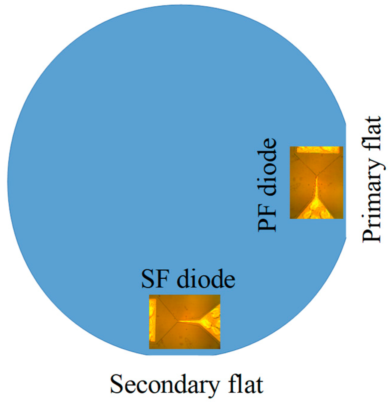
2. Samples and Methods

The modulation-doped GaAs/AlGaAs semiconductor structure with a wide i-AlGaAs spacer was chosen as a base material for the fabrication of symmetrically and asymmetrically shaped bow-tie microwave diodes. A cross-section of the MBE-grown active region of the modulation-doped structure and the energy band diagram are presented in Figure 1. A two-dimensional electron gas channel was formed in the unintentionally doped i-GaAs layer near the interface with a 45 nm thick i-Al0.25Ga0.75As spacer, transferring electrons from the homogeneously doped 80 nm thick n+-Al0.25Ga0.75As barrier layer. It should be noted that the electron density in the doped AlGaAs barrier was of the same order of magnitude as that in the GaAs channel. Approximately 30 periods of i-GaAs/i-AlGaAs superlattice served as a buffer layer between the semi-insulating GaAs (100) substrate and the MBE-grown active layer of the modulation-doped structure (not shown in Figure 1).
The semiconductor mesa structure of the bow-tie diodes was formed by wet etching to a ~200 nm depth, and the metallic contacts were then shaped within the limits of the mesa structure (Figure 2). Based on the geometric shape of the mesa structure, symmetric (SD) and asymmetric (AD) bow-tie diodes were manufactured and studied. Micrographs of the diodes are presented in Figure 2.
Depending on the narrowest part of the bow-tie diodes (the neck), we further denoted the diodes as ADi or SDi, with index i representing the width d of the neck in micrometers (i = 1,2,3). The diodes were manufactured in the following two orientations: with the longitudinal axis of symmetry oriented along the cuts of the primary flat (PF diode) and the secondary flat (SF diode) of the semiconductor substrate. A schematic view of the p-type GaAs substrate with the primary and secondary flats and the bow-tie diodes oriented along the corresponding cuts is presented in Figure 3.
The detailed fabrication process of the bow-tie diodes was described in our previous work [21]. Due to the need to collect extensive statistical data, we conducted the measurements using probe stations. The Suss MicroTec probe station EP6 with DC probes (FormFactor, Inc., Livermore, CA, USA) and the Agilent E5270B precision measurement equipment (Agilent Technologies, Inc., Santa Clara, CA, USA) were used to measure the current–voltage (I-V) characteristics. A Cascade Microtech (FormFactor, Inc., Livermore, CA, USA) high-frequency probe station was operated to obtain high-frequency measurements of the dependence of the detected voltage on microwave power and frequency. ACP40-A-GS-250 and I110-A-GS-150 probes were used to connect the bow-tie diodes to the measurement station in the Ka and W frequency ranges, respectively. The DC voltage signal induced across the diodes was separated from the microwave signal in the Ka and W frequency ranges using SHF BT45 and SHF BT110 broadband bias tees, respectively. The millimeter-wave sweep generators G4408E and G4403E (Elmika, Inc., Vilnius, Lithuania) served as sources of microwave radiation in the Ka and W frequency ranges. To clarify the nature of the voltage detected across the diodes, all their electrical parameters were measured in the dark and under illumination from a white light source or an infrared-emitting diode. As a source of white light, the Eiko EKE21V150W photolamp (color temperature 3240 K) at the maximum illuminance of 14,000 lx was used. An IR333/H2 (peak wavelength 940 nm and 1000 lx illuminance) LED was used as the infrared light emitter. The spectra of the photolamp and IR LED are presented in Figure A1 of the Appendix A.
The photoluminescence measurements were carried out using a standard photoluminescence setup with a 1 m FHR1000 monochromator and a thermoelectrically cooled GaAs photomultiplier tube operating in a photon-counting regime. An Ar-ion laser (2.4–2.7 eV) with the vertical linear polarization (≥100:1) and the intensity kept at 0.63 W/cm2 irradiated the surface of the sample at an angle of 18°. To change the temperature, the sample was mounted in a closed-cycle helium optical cryostat. Additionally, two Glan–Taylor prisms were placed in front of the monochromator entrance slit. The first one was used as a polarization analyzer, and the second one was rotated at a magic angle to minimize the polarization effects of the monochromator grating. A conventional in-plane polarized PL was measured from the (100) sample surface.

3. Results

In the first subsection, we present the photoluminescence studies of modulation-doped structures, examining their dependence on the polarization of light used to excite charge carriers. A statistical review of the voltage sensitivity of various bow-tie diodes is presented in the next subsection. This subsection also reviews the voltage detected across the bow-tie diodes under different illumination conditions.

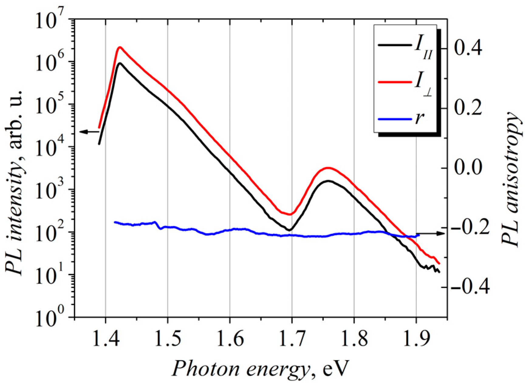
3.1. Photoluminescence Anisotropy of the Modulation-Doped GaAs/AlGaAs Structure

Three quantities can be used to describe the polarization-dependent characteristics. These are polarization P, anisotropy r, and depolarization degree ρ [22]. All these parameters are interrelated, and therefore each of them can be expressed through each other. In most cases, r is a more meaningful parameter and is expressed as follows [23]:
r = I I I I I I I + 2 I = 3 c o s 2 α 1 5
where I I I and I are the emission intensities measured by orienting the Glan–Taylor prism in two parallel and perpendicular positions relative to the laser polarization, respectively, and α is the angle between the absorption and emission dipoles. The limits of anisotropy in completely oriented systems range from +1 to −0.5. Here, 0 stands for the unpolarized emission, +1 means that the emitted light polarization is entirely parallel, and −0.5 means that it is completely perpendicular to the excitation polarization. For a randomly oriented ensemble, the limits of anisotropy are +0.4 to −0.2. The linearly polarized PL spectra of the structure emitted from the (100) surface at 300 K are shown in Figure 4. The photoluminescence anisotropy r is shown here. Notably, the anisotropy value is around −0.2 (varies from −0.17 to −0.24) across the measured spectrum. This means that the polarization of the emitted light is perpendicular to the laser polarization. This is true for free electron–heavy hole transitions in the case of excitation with linearly polarized light [24].

3.2. Voltage Sensitivity of the Bow-Tie Diodes

The voltage sensitivity S of a detector is the ratio between the voltage U d detected by the diode and the microwave power P incident on the diode, as follows:
S = U d P
The voltage sensitivity of the bow-tie diodes was measured at a frequency of 30 GHz within the microwave power range where the detected voltage U d varies linearly with the microwave power P . Histograms of the mean values of the bow-tie diodes’ voltage sensitivity, oriented along the primary and secondary flats, are presented in Figure 5a and Figure 5b, respectively. The polarity of the detected voltage in both the PF and SF diodes corresponds to the polarity of the thermoelectric emf (TEMF) of the hot electrons, i.e., the negative potential is induced on the metalized side (left side in Figure 2) of the bow-tie diode. Hereafter, the detected voltage and voltage sensitivity will be represented with a positive sign corresponding to the polarity of the hot electron TEMF. The voltage sensitivity of the PF diodes correlated with the diode neck’s width d , both for symmetric and asymmetric diodes, i.e., it showed a tendency to decrease with a wider neck. Furthermore, the voltage sensitivity of asymmetric diodes was higher than that of symmetric ones, in agreement with the following analytically derived formula for the voltage sensitivity of the bow-tie microwave diode operating on the basis of the hot carrier phenomenon [19]:
S = 2 R s h μ 0 t a n γ 3 d 2 l n a d P P i N
Here, R s h denotes the sheet resistance of the modulation-doped semiconductor structure, μ 0 is the weak-field electron mobility, γ denotes the widening angle of the active part of the diode, a and d represent the width in the widest and narrowest parts of the diode, respectively (see Figure 2), P i and P denote the microwave power incident on and absorbed by the diode, respectively, and N is a factor dependent on frequency and relaxation time constants [25]. In the case of the PF diodes, the measured voltage sensitivity qualitatively corresponded to the value calculated according to Formula (3), whereas the voltage sensitivity of the symmetric SF diodes was higher than that of the asymmetric ones. A comparison of the S values of the PF and SF diodes allowed us to conclude that the orientation of the diodes was important for the asymmetric ones; within the limits of statistical error, the voltage sensitivity of the SD diodes was the same both for the PF and SF diodes, while the sensitivity of the diodes was lower than that of the AD-PF diodes. As mentioned, the nature of the voltage detected by the bow-tie diodes is based on the heating of the charge carriers in a microwave electric field. Therefore, different heating conditions may depend on the electric field orientation with respect to the crystallographic axes. This proposition is especially applicable for the electrons of the n+ doped barrier layer (see Figure 1), since their heating may result in the stronger conduction anisotropy due to stronger influence of the higher energy X and L valleys in the doped AlGaAs barrier layer [26].
Another distinguishing feature of the PF and SF diodes is their different responses to illumination. As shown in Figure 5, the white light enhances the voltage sensitivity of the PF bow-tie diodes, while the SF diodes are more sensitive to the microwave radiation in the dark. This difference is visualized in Figure 6.
In the dark, the symmetric PF diodes are less sensitive to microwave radiation than the SF ones. White light illumination of the symmetric bow-tie diodes makes their sensitivity independent of orientation. Asymmetric PF diodes are approximately twice as sensitive in the dark than the SF diodes, and the illumination increases this difference. Also, the sensitivity difference between the asymmetric PF and SF diodes increases as the diode neck’s width d decreases. This may mean that PF diodes, with their longitudinal axis of symmetry oriented along the primary flat cut, exhibit an additional detection mechanism related to electron heating, which we do not observe in the case of SF diodes. Such voltage sensitivity anisotropy can be attributed to the involvement of electrons from the higher L and X valleys in the electrical conduction. This fact becomes more prominent when electrons are transferred to the higher valleys by the illumination. As is known, at a certain orientation of the electric field with respect to the crystallographic axes, the so-called intervalley electron diffusion may occur due to the different drift velocities of the hot electrons in different valleys [27]. Intervalley diffusion of hot electrons leads to the separation of the electron charge in space and the appearance of the intervalley emf in a many-valley semiconductor; this emf was observed experimentally [28]. The intervalley electron scattering, like any relaxation process, is characterized by its frequency dependence. Therefore, in the next section, we examine the dependence of the voltage sensitivity on the microwave frequency in PF and SF bow-tie diodes.

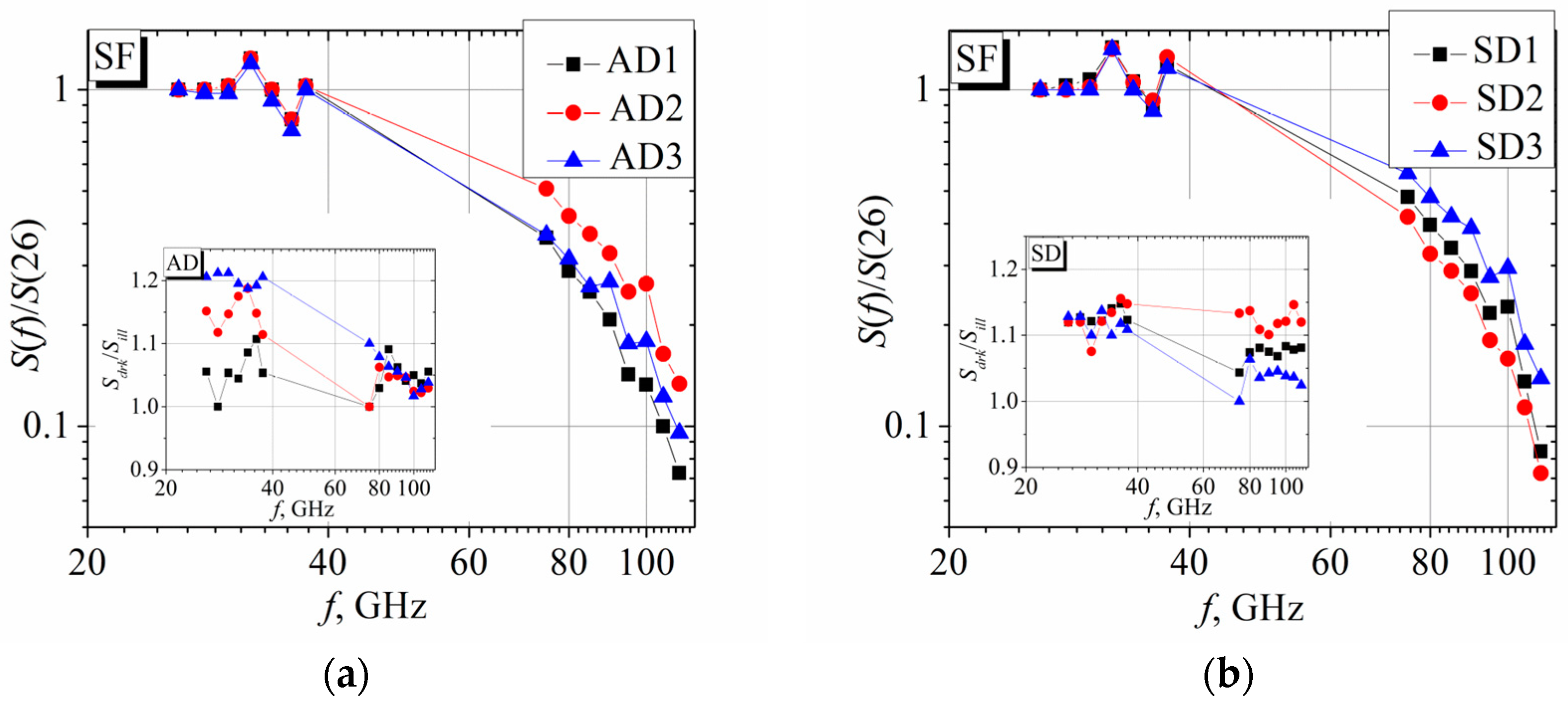
3.3. Frequency Dependence of the Voltage Sensitivity in Differently Oriented Bow-Tie Diodes

Figure 7 shows the dependence of the relative voltage sensitivity of asymmetric (a) and symmetric (b) PF bow-tie diodes on frequency.
The insets reveal the influence of illumination on voltage sensitivity. It is worth noting that both the symmetrical and asymmetrical bow-tie diodes with the narrowest neck exhibit a stronger dependence of the sensitivity on the frequency within the W frequency range (from 75 to 110 GHz). As the insets of Figure 7 show, an increase in the sensitivity ratio is seen in the cases of both the asymmetric and symmetric bow-tie diodes. Moreover, the ratio is higher for the narrower-necked SD bow-tie diodes. The electric field strength E in the narrowest part of the SD bow-tie diode is stronger than that of the AD diode under the same applied voltage value U and the same neck width d , as can be seen from the following formula [25]:
E = 2 U d l n a d
The stronger the electric field, the more intense the heating of the charge carriers, and the more efficient their redistribution to the higher valleys. As a result, the difference between the voltage sensitivity of the “dark” and illuminated diodes is more pronounced.
The frequency dependence of the relative voltage sensitivity of the bow-tie diodes oriented parallel to the secondary flat cut are presented in Figure 8. The ratio of the voltage sensitivity of the “dark” and illuminated diodes is displayed in the insets.
The main difference between the frequency dependencies of the voltage sensitivity of the PF and SF bow-tie diodes is expressed in their response to light. The insets show that the response of the SF diodes to illumination is weaker and, significantly, the illumination reduces the voltage sensitivity. In contrast with the case of the PF diodes (Figure 7), the ratio S d r k / S i l l of the asymmetric bow-tie SF diodes decreases with a higher microwave frequency. At low frequencies, this ratio decreases with narrower diode necks; at high frequencies, it becomes almost independent of the AD diode neck. The symmetrical SF diodes show similar values of the S d r k / S i l l ratio, and the only difference is that it is almost independent of the neck’s width at low frequencies and is slightly scattered at high frequencies, which, however, has a stochastic character.
The frequency dependence of the voltage sensitivity S presented in Figure 7 and Figure 8 can be approximated using the following expression characterizing the dependence of the intervalley emf on the frequency of the microwave radiation [28]:
S = S 0 1 1 + ω τ i n t 2
where S 0 represents the voltage sensitivity at low frequency, ω is the angular frequency, and τ i n t denotes the intervalley relaxation time constant.
A more detailed derivation of the expression for the voltage sensitivity of a point diode due to the intervalley phenomena [28] is provided in Appendix C. The frequency dependence of the sensitivity is independent of the microwave diode design. Assuming that the approximated values of τ i n t weakly depend on the width d of the bow-tie diode’s neck, we obtain the average intervalley relaxation times for the AD and SD diodes with their longitudinal axes oriented along the primary and secondary flat cuts (see Table 1).
For comparison, the value of τ i n t equal to 10 picoseconds was obtained from the microwave noise measurements in the GaAs/AlAs/GaAs heterostructure at liquid nitrogen temperature [29]. The lower values of the time constant obtained in our room temperature investigation can be explained by the fact that the relaxation processes in semiconductors take longer with lower temperatures [30].

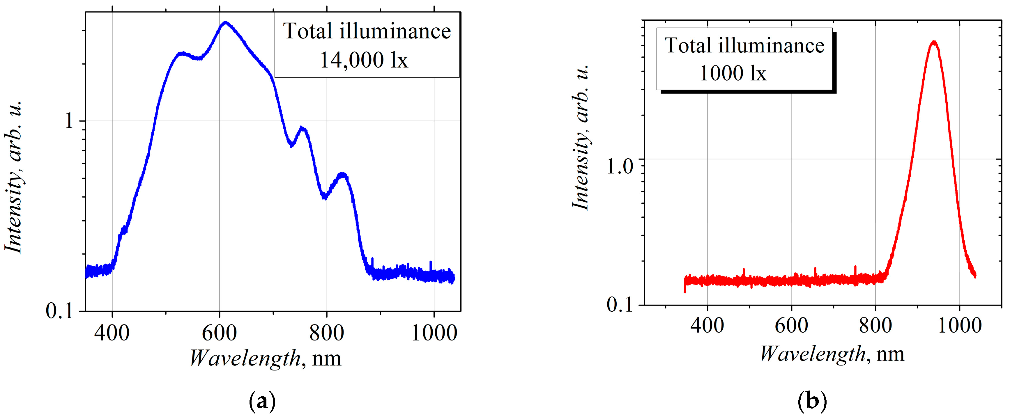
3.4. Influence of Illumination on the Electrical Properties of Bow-Tie Diodes

A white light was used in addition to the microwave radiation in the research presented above. The photon energy was sufficient to transfer electrons from the valence to the conduction band. However, it is known that deep energy impurity centers, called DX centers, may exist in the bandgap of the AlxGa1−xAs compound when the AlAs mole fraction x exceeds 0.2 [31]. Therefore, further experiments were performed with the bow-tie diodes illuminated using infrared radiation with photon energy below the bandgap. We used an LED with a peak photon energy of 1.32 eV, which was lower than the energy bandgap of GaAs at room temperature [30].
The ratio of the voltage sensitivities measured in the dark and under the illumination of the AD and SD bow-tie diodes with their longitudinal axes parallel to the primary flat cut are presented in Figure 9. It can be seen that the infrared light has a stronger increasing impact on the voltage sensitivity of the asymmetric PF bow-tie diodes than the white light. The IR radiation increases the sensitivity by up to 1.5 times in the case of the AD diodes, and this increase reaches almost two times in the case of the SD diodes. The influence of illumination from the different light sources on the voltage sensitivity of the bow-tie diodes that are oriented along the secondary flat cut is depicted in Figure 10.
In this case, both types of illumination reduced the voltage sensitivity of the AD and SD bow-tie diodes. However, the sensitivity of the symmetric bow-tie diodes experienced a more pronounced reduction with the IR radiation, while the white light had a stronger impact on the voltage sensitivity of the asymmetric diodes, as can be seen in Figure 10.
The influence of the white and infrared light on the voltage dependence of the electrical resistance of the PF and SF diodes is shown in Figure 11.
A common feature of the dependence of the relative resistance on the voltage in the dark is that in the forward direction (the negative potential is on the side of the thinner metallization), the resistance increases for both the PF and SF diodes. In the direction of the reverse voltage, the resistance decreases, and for PF diodes, it begins to increase slightly at higher values of the applied voltage. Illumination of the PF diode accelerates the growth of its resistance with increasing the voltage for both polarities of the applied voltage, as well as when a reverse voltage is applied to the SF diode. When a forward voltage is applied to an SF diode, we observe the inverse relationship, where the diode’s resistance decreases under illumination. The resistance of the PF diode is the least affected by the illumination when a voltage is applied to the diode in the forward direction. In other cases, the influence of illumination on the diode resistance is significant, and white light changes the diode resistance more than infrared radiation. For a typical bow-tie diode with an n n + junction, the resistance increases with both polarities of the applied voltage due to the decrease in the electron mobility in strong electric fields [32]. However, as we have found in our previous work [19], the dependence of the resistance on the electric field strength in a bow-tie diode on the basis of the modulation-doped structure with a wide spacer is not described solely by the decrease in electron mobility in a strong electric field but also by the change in electron density as they move through the diode. For a bow-tie diode, whose detection properties are based on the emergence of a hot electron electromotive force in a strong microwave electric field, the asymmetry of the diode’s current–voltage characteristic correlates with the diode’s voltage sensitivity [21]. However, as we can see from Figure 11, the resistance in the reverse current direction of the studied bow-tie diodes in the dark is lower than the resistance in the reverse direction for both PF and SF diodes. Only when the SF diodes are illuminated with infrared radiation do we observe the “correct” polarity of the I-V asymmetry, when the resistance in the forward direction is lower than in the reverse direction (see Figure 11b). Therefore, we should state that the I-V characteristic of bow-tie diodes is determined by the slow electron capture phenomena, which do not affect the voltage detected by the diodes. In other words, the voltage detected by the bow-tie diodes is not the result of microwave current smoothing, but rather the sum of the hot electron electromotive force and the intervalley electromotive force, respectively, in the doped AlGaAs barrier and the GaAs two-dimensional electron gas channel.

4. Conclusions

The research conducted in this work allows us to state that the direction of the electric field heating electrons in a modulation-doped semiconductor structure with respect to the crystallographic axes influences the detection properties of bow-tie diodes based on this semiconductor structure. The following more detailed conclusions can also be made:
  • In the dark, the microwave voltage sensitivity of the bow-tie diodes with their longitudinal axis oriented along the primary flat cut of GaAs(100) substrate (PF diodes) is higher for asymmetric bow-tie diodes than for symmetric ones, and vice versa. The voltage sensitivity of the diodes oriented perpendicular to this direction (SF diodes) is higher for symmetric diodes.
  • Illumination affects the PF and SF diodes differently. If the voltage sensitivity of the PF bow-tie diodes increases when illuminated, the voltage sensitivity of the SF diodes decreases when exposed to light.
  • Asymmetric PF diodes are several times more sensitive to microwave radiation than symmetric bow-tie diodes.
  • The frequency dependence of the voltage sensitivity of the PF and SF diodes are similar in the Ka and W frequency ranges; a decrease in the voltage sensitivity with a time constant of several picoseconds is observed.
  • When comparing the effects of the illumination of the diodes using white light and infrared radiation, in most cases, we observe a greater influence of the infrared red radiation on the voltage sensitivity of the diodes, while the resistance of the diodes changes more noticeably under white light illumination.
  • Therefore, we attribute these changes in the electrical parameters of the bow-tie diodes under the influence of the illumination to the emission of electrons from the energy gap of the AlGaAs barrier layer into the conduction band.
  • Finally, a comparison of the research results regarding bow-tie diodes oriented perpendicular to each other with respect to the crystallographic axes allows us to state that the nature of the voltage detected in the microwaves in the bow-tie diodes lies in the heating of electrons in both the AlGaAs barrier and the GaAs channel. The heating of electrons in the barrier layer determines the different detection properties of the diodes due to the redistribution of electrons in higher energy valleys.
  • We hope this article will inspire further research into the anisotropic properties of bow-tie diodes, as some questions regarding the nature of the detected voltage remain unanswered. We also aim to initiate fruitful discussions on this topic.
  • Further studies on bow-tie diodes based on modulation-doped semiconductor structures could be carried out by minimizing the influence of the doped barrier layer and, as an instrument, using a wider variety of light sources to modify the detection properties of bow-tie diodes.

Author Contributions

Conceptualization, A.S. and S.A.; methodology, A.S., S.A., M.A. and J.G.; simulations, A.S. and A.L.; microwave investigation, A.S., M.A., and A.L.; photoluminescence investigations, A.Č.; illumination experiments, A.L. and I.Z.; writing—original draft preparation, A.S.; writing—review and editing, S.A., A.Č. and J.G.; visualization, A.S. and J.G.; supervision, A.S.; project administration, J.G.; spectral experiments, I.Z. All authors have read and agreed to the published version of the manuscript.

Funding

This research received no external funding.

Informed Consent Statement

Not applicable.

Data Availability Statement

The original contributions presented in the study are included in the article; further inquiries can be directed to the corresponding author.

Acknowledgments

Authors acknowledge Hadas Shtrikman from the Braun Center for Submicron Research at the Weizmann Institute of Science, Rehovot, Israel, for MBE-grown structures that were used for sample preparation. We are extremely grateful to Romanas Sedlickas for editing the manuscript.

Conflicts of Interest

The authors declare no conflicts of interest.

Appendix A

Spectra of photolamp Eiko EKE21V150W and infrared light emitting diode IR333/H2.
Figure A1. Spectra of photo-lamp (a) and infrared light emitting diode (b).
Crystals 15 00367 g0a1

Appendix B

Comparison of the voltage sensitivity and the low-field electrical resistance of the bow-tie diodes with the longitudinal axis oriented alongside the primary and secondary flats.
Table A1. Voltage sensitivity of the bow-tie diodes with the longitudinal axis oriented alongside primary (PF) and secondary (SF) flats.
OrientationDiodeIlluminationNumber of Measured DiodesSmean, V/W Smedian, V/WStD, V/WStD/Smean, %
PFSD1white100.660.660.2234
dark100.400.380.1846
SD2white100.470.530.1837
dark100.310.330.1240
SD3white110.390.420.1127
dark110.300.320.0827
AD1white111.401.400.4230
dark110.750.570.3749
AD2white110.800.740.2632
dark110.510.440.3262
AD3white110.710.740.1520
dark110.520.530.1325
SFSD1white90.630.690.2540
dark90.680.750.2740
SD2white90.470.470.049
dark90.520.510.059
SD3white90.390.390.0411
dark90.420.400.0512
AD1white110.320.440.40126
dark110.340.470.39116
AD2white130.280.320.1449
dark130.320.350.1443
AD3white180.310.310.1033
dark180.340.360.1131
Table A2. Low-field electrical resistance of the bow-tie diodes with longitudinal axis oriented alongside primary and secondary flats.
OrientationDiodeIlluminationNumber of Measured DiodesR(0)mean, V/W R(0)median, V/WStD, V/WStD/R(0)mean, %Calculated, R(0) kΩ(R(0)mean-Rcalc.)/R(0) calc.. %
PFSD1white1111.811.870.544.611.354
dark1114.8415.251.167.812.2421
SD2white99.589.590.141.59.362
dark912120.322.710.119
SD3white108.418.390.161.98.420
dark1010.4110.610.454.39.0915
AD1white104.424.430.143.23.143
dark105.485.490.264.73.3464
AD2white113.53.50.12.92.5836
dark114.34.340.184.22.854
AD3white113.13.110.051.62.3234
dark113.83.820.12.62.5251
SFSD1white811.2511.150.474.1711.35−10
dark813.3013.200.392.9512.24106
SD2white99.709.600.202.069.3634
dark911.2811.300.322.8310.1118
SD3white98.568.500.192.208.4214
dark99.9710.000.262.619.0988
AD1white103.733.750.112.893.163
dark104.414.500.194.423.34107
AD2white133.193.210.092.732.5861
dark133.713.750.164.252.891
AD3white182.832.920.279.662.3251
dark183.293.360.329.852.5277

Appendix C

Derivation of the voltage sensitivity expression for the AlGaAs/GaAs point-contact diode, considering the intervalley scattering phenomena. The voltage sensitivity of the AlGaAs/GaAs point-contact diode [28], where the intervalley emf U i n t I I arises between the contacts, is given by the following:
S = U i n t I I P i
where P i is the microwave power incident on the diode.
However, only a part of the incident microwave power is absorbed by the microwave diode. Let us introduce the factor K that indicates what part of the incident microwave power is absorbed by the diode as follows:
K = P a b s P i
where P a b s marks the microwave power absorbed by the diode, as expressed in the following equation:
P a b s = I 2 R = e n μ E 2 π r 0 2 2 h e n μ π r 0 2 = π e n μ E 2 r 0 2 h
where I is the current strength across the diode, R notes the electrical resistance of the diode, E represents the electric field strength, r 0 is the radius of the contact, and h stands for the thickness of the AlGaAs layer.
The electron mobility μ x in a two-valley semiconductor in the direction of the applied electric field is expressed as follows:
μ x = n 0 ( 1 ) μ x 0 ( 1 ) + n 0 ( 2 ) μ x 0 ( 2 ) n 0
where n 0 is the electron density, and the superscript indexes note the valley numbers.
The intervalley electromotive force U i n t I I is as follows:
U i n t I I = V k D ¯ i n t I I μ 0 D 0 μ x
where D ¯ i n t I I stands for the averaged intervalley electron diffusion coefficient, and V k denotes the contact voltage, as follows:
V k = k T 0 e l n n + n
where k is the Boltzmann’s constant, T 0 denotes the temperature, and n + and n represent the electron density in the heavily and lightly doped regions of the n+/n junction, respectively.
The electron intervalley diffusion coefficient averaged over the period of the microwave signal of frequency ω is calculated as follows:
D ¯ i n t I I = 1 2 π 0 2 π D i n t I I E d ω t
In the case of two valleys, the intervalley electron diffusion coefficient is found as follows:
D i n t I I = n ( 1 ) n ( 2 ) n 2 μ ( 1 ) μ ( 2 ) 2 E 2 τ i n t 1 + ω τ i n t 2
where τ i n t denotes the intervalley relaxation time constant. When the microwave electric field strengths E varies harmonically, integrating Equation (A7) yields the following expression:
D ¯ i n t I I = n 1 n 2 2 n 2 μ 1 μ 2 2 E 2 τ i n t 1 + ω τ i n t 2
Substituting D ¯ i n t I I from Equation (A9) into Equation (A5) and considering Einstein’s relation, we obtain the following expression of the detected intervalley voltage:
U i n t = n 1 n 2 2 μ x n 2 μ 1 μ 2 2 E 2 τ i n t 1 + ω τ i n t 2 l n n + n
Now, we are ready to calculate the voltage sensitivity of the point-contact diode after substituting the Equations (A2), (A3), and (A10) into Equation (A1), as follows:
S = n 1 n 2 μ 1 μ 2 2 τ i n t 2 π n 2 n ( 1 ) μ ( 1 ) + n ( 2 ) μ ( 2 ) r 0 2 h E 0 E 2 K 1 1 + ω τ i n t 2 = S 0 1 1 + ω τ i n t 2
where S 0 stands for the voltage sensitivity at low frequency.

References

  1. Jacoboni, C.; Reggiani, L. Bulk hot-electron properties of cubic semiconductors. Adv. Phys. 1979, 28, 493–553. [Google Scholar] [CrossRef]
  2. Gaylord, T.K.; Rabson, T.A. Anisotropy in the Conductivity of N-Gallium Arsenide. Phys. Lett. A 1970, 33, 95–96. [Google Scholar] [CrossRef]
  3. Gaylord, T.K.; Rabson, T.A. Determination of Conduction Anisotropies in Semiconductors. Solid-State Electron. 1972, 15, 953–960. [Google Scholar] [CrossRef]
  4. Kalevich, V.K.; Zakharchenya, B.P.; Fedorova, O.M. Strong anisotropy of the conduction-electron g-factor in GaAs/AlGaAs quantum wells. Phys. Solid State 1995, 37, 154–156. Available online: https://www.researchgate.net/publication/252641982 (accessed on 3 March 2025).
  5. Cole, B.E.; Batty, W.; Imanaka, Y.; Shimamoto, Y.; Singleton, J.; Chamberlain, J.M.; Miura, N.; Henini, M.; Cheng, T. Effective-mass anisotropy in GaAs-(Ga,Al)As twodimensional hole systems: Comparison of theory and very high-field cyclotron resonance experiments. J. Phys. Candens. Mater 1995, 7, L675–L681. [Google Scholar] [CrossRef]
  6. Nakamura, Y.; Koshiba, S.; Sakaki, H. Large conductance anisotropy in a novel two-dimensional electron system grown on vicinal (111)B GaAs with multiatomic steps. Appl. Phys. Lett. 1996, 69, 4093–4095. [Google Scholar] [CrossRef]
  7. Petit, F.; Lelarge, F.; Cavanna, A.; Laruelle, F.; Etienne, B. Enhancement of electron conductivity in GaAs/AlAs coupled quantum wires. Physica E 1998, 2, 933–939. [Google Scholar] [CrossRef]
  8. Kwok, S.H.; Grahn, H.T.; Ploog, K.; Merlin, R. Giant Electropleochroism in GaAs-(Al, Ga) As Heterostructures: The Quantum-Well Pockels Effect. Phys. Rev. Lett. 1992, 69, 973–976. [Google Scholar] [CrossRef]
  9. Shalygin, V.A.; Makhov, I.S.; Adamov, R.B.; Vinnichenko, M.Y.; Khvostikov, V.P.; Firsov, D.A. Electric-field-induced polarization anisotropy of interband photoluminescence in GaAs. J. Appl. Phys. 2024, 136, 195703. [Google Scholar] [CrossRef]
  10. Im, H.; Klipstein, P.C.; Grey, R.; Hill, G. Rotation of the Conduction Band Valleys in AlAs due to XX-XY Mixing. Phys. Rev. Lett. 1999, 83, 3693–3696. [Google Scholar] [CrossRef]
  11. Reker, T.; Im, H.; Bremme, L.E.; Choi, H.; Chung, Y.; Klipstein, P.C.; Shtrikman, H. Effective Mass Anisotropy of Γ Electrons in GaAs/AlGaAs Quantum Wells. Phys. Rev. Lett. 2002, 88, 056403. [Google Scholar] [CrossRef] [PubMed]
  12. Vdovin, E.E.; Khanin, Y.N.; Dubrovskii, Y.V.; Main, P.C.; Eaves, L.; Henini, M.; Hill, G. Probing the effective mass anisotropy of G electrons in a GaAsÕ.AlGa.As quantum well. Phys. Rev. B 2003, 67, 205305. [Google Scholar] [CrossRef]
  13. Balocchi, A.; Amand, T.; Wang, G.; Liu, B.L.; Renucci, P.; Duong, Q.H.; Marie, X. Electric field dependence of the spin relaxation anisotropy in (111) GaAs/AlGaAs quantum wells. New J. Phys. 2013, 15, 095016. [Google Scholar] [CrossRef]
  14. Luckyanova, M.N.; Johnson, J.A.; Maznev, A.A.; Garg, J.; Jandl, A.; Bulsara, M.T.; Fitzgerald, E.A.; Nelson, K.A.; Chen, G. Anisotropy of the Thermal Conductivity in GaAs/AlAs Superlattices. Nano Lett. 2013, 13, 3973–3977. [Google Scholar] [CrossRef]
  15. Sisodia, N.; Muduli, P.K. Enhancement of microwave detection sensitivity in un-biased perpendicular magnetic tunnel junctions using voltage controlled magnetic anisotropy. J. Magn. Magn. Mater. 2020, 515, 167301. [Google Scholar] [CrossRef]
  16. Jorudas, J.; Seliuta, D.; Minkevičius, L.; Janonis, V.; Subačius, L.; Pashnev, D.; Pralgauskaitė, S.; Matukas, J.; Ikamas, K.; Lisauskas, A.; et al. Terahertz bow-tie diode based on asymmetrically shaped AlGaN/GaN heterostructures. Lith. J. Phys. 2023, 63, 191–201. [Google Scholar] [CrossRef]
  17. Seliuta, D.; Vyšniauskas, J.; Ikamas, K.; Lisauskas, A.; Kašalynas, I.; Reklaitis, A.; Valušis, G. Symmetric bow-tie diode for terahertz detection based on transverse hot-carrier transport. J. Phys. D Appl. Phys. 2020, 53, 275106. [Google Scholar] [CrossRef]
  18. Valušis, G.; Lisauskas, A.; Yuan, H.; Knap, W.; Roskos, H.G. Roadmap of Terahertz Imaging 2021. Sensors 2021, 21, 4092. [Google Scholar] [CrossRef]
  19. Ašmontas, S.; Anbinderis, M.; Čerškus, A.; Gradauskas, J.; Lučun, A.; Sužiedėlis, A. Microwave Bow-Tie Diodes on Bases of 2D Semiconductor Structures. Crystals 2024, 14, 720. [Google Scholar] [CrossRef]
  20. Sužiedėlis, A.; Ašmontas, S.; Gradauskas, J.; Čerškus, A.; Šilėnas, A.; Lučun, A. Impact of Buffer Layer on Electrical Properties of Bow-Tie Microwave Diodes on the Base of MBE-Grown Modulation-Doped Semiconductor Structure. Crystals 2025, 15, 50. [Google Scholar] [CrossRef]
  21. Sužiedėlis, A.; Ašmontas, S.; Gradauskas, J.; Čerškus, A.; Anbinderis, M. Indirect measurement of electron energy relaxation time at room temperature in two dimensional heterostructured semiconductors. Materials 2022, 15, 3224. [Google Scholar] [CrossRef] [PubMed]
  22. Kawski, A. Fluorescence Anisotropy: Theory and Applications of Rotational Depolarization. Crit. Rev. Anal. Chem. 1993, 23, 459–529. [Google Scholar] [CrossRef]
  23. Ameloot, M.; vandeVen, M.; Acuña, A.U.; Valeur, B. Fluorescence anisotropy measurements in solution: Methods and reference materials (IUPAC technical report). Pure Appl. Chem. 2013, 85, 589–608. [Google Scholar] [CrossRef]
  24. Zakharchenya, B.P.; Mirlin, D.N.; Perel’, V.I.; Reshina, I.I. Spectrum and polarization of hot-electron photoluminescence in semiconductors. Sov. Phys. Uspekhi 1982, 25, 143–166. Available online: https://iopscience.iop.org/article/10.1070/PU1982v025n03ABEH004519 (accessed on 3 March 2025). [CrossRef]
  25. Sužiedėlis, A.; Ašmontas, S.; Gradauskas, J.; Čerškus, A.; Požela, K.; Anbinderis, M. Competition between Direct Detection Mechanisms in Planar Bow-Tie Microwave Diodes on the Base of InAlAs/InGaAs/InAlAs Heterostructures. Sensors 2023, 23, 1441. [Google Scholar] [CrossRef]
  26. Bhattacharya, P. The relationship of the D-X centre in AlxGa1-xAs and other III-V alloys with the conduction band structure. Semicond. Sci. Technol. 1988, 3, 1145–1156. [Google Scholar] [CrossRef]
  27. Canali, C.; Jacoboni, C.; Nava, F. Intervalley Diffusion of Hot Electrons in Germanium. Solid State Commun. 1978, 26, 889–892. [Google Scholar] [CrossRef]
  28. Sužiedėlis, A.; Ašmontas, S.; Kundrotas, J.; Nargelienė, V.; Gradauskas, J. Voltage sensitivity of a point-contact GaAs/AlGaAs heterojunction microwave detector. Phys. Scr. 2012, 85, 035702. [Google Scholar] [CrossRef]
  29. Hartnagel, L.; Katilius, R.; Matulionis, A. Microwave Noise in Semiconductor Devices; Wiley: New York, NY, USA, 2001; 312p. [Google Scholar]
  30. Dargys, A.; Kundrotas, J. Handbook on Physical Properties if Ge, Si, GaAs and InP; Science and Encyclopedia Publishers: Vilnius, Lithuania, 1994; 264p, Available online: https://openlibrary.org/books/OL295382M/Handbook_on_physical_properties_of_Ge_Si_GaAs_and_InP (accessed on 3 March 2025).
  31. Mooney, P.M. Deep donor levels(DX centers) inIII-V semiconductors. J. Appl. Phys. 1990, 67, R1–R26. [Google Scholar] [CrossRef]
  32. Conwell, E.M. High Field Transport in Semiconductors; Academic Press: New York, NY, USA; London, UK, 1967; 293p. [Google Scholar]
Figure 1. Cross-section and energy band diagram (blue lines) and electron density (red lines) in the active region of the modulation-doped semiconductor structure used to fabricate the bow-tie diodes.
Crystals 15 00367 g001
Figure 2. Micrographs of symmetric SD (a) and asymmetric AD (b) bow-tie diodes. Notations in the drawing: MDS stands for modulation doped structure; Ge-Ni-Au are ohmic contacts; d notes the width of the diode neck; a and b are the maximum width of AD and SD diodes, respectively; γ denotes the widening angle of the active part of the diode.
Crystals 15 00367 g002
Figure 3. Schematic view of p-type GaAs substrate with primary and secondary flats and PF and SF bow-tie diodes oriented along the corresponding cuts.
Crystals 15 00367 g003
Figure 4. Linearly polarized PL spectra and its anisotropy at 300 K.
Crystals 15 00367 g004
Figure 5. Statistical representation of voltage sensitivity of symmetrically (SD) and asymmetrically (AD) shaped bow-tie diodes with their longitudinal axles oriented along primary (a) and secondary (b) substrate flats. Numbers below the corresponding columns mean the width d of the bow-tie diode’s neck. The illuminated diodes were exposed to the white light.
Crystals 15 00367 g005
Figure 6. The ratio of voltage sensitivity of symmetric and asymmetric bow-tie diodes oriented along primary (PF) and secondary (SF) flat cuts in the dark (drk) and illuminated (ill) case as a function of diode neck’s width.
Crystals 15 00367 g006
Figure 7. Frequency dependence of PF diodes’ voltage sensitivity relative to the sensitivity value at f = 26 GHz for the asymmetric (a) and symmetric (b) diodes. The ratio of voltage sensitivity of illuminated and unilluminated (“dark”) diodes is presented in the insets.
Crystals 15 00367 g007
Figure 8. Frequency dependence of SF diodes’ voltage sensitivity relative to the sensitivity value at f = 26 GHz for the asymmetric (a) and symmetric (b) diodes. The ratio of voltage sensitivity of illuminated and unilluminated (“dark”) diodes is presented in the insets.
Crystals 15 00367 g008
Figure 9. Dependence of the relative (illuminated case versus dark case) voltage sensitivity on microwave power of the asymmetric (a) and symmetric (b) PF bow-tie diodes. For the illumination, either white light or infrared radiation were used.
Crystals 15 00367 g009
Figure 10. Dependence of the relative (dark case versus illuminated case) voltage sensitivity on microwave power of the asymmetric (a) and symmetric (b) SF bow-tie diodes. For the illumination, either white light or infrared radiation were used.
Crystals 15 00367 g010
Figure 11. Dependence of the relative resistance of PF- (a) and SF- (b) oriented AD1 bow-tie diodes on applied voltage in the dark and under illumination of IR and white light. R ( 0 ) stands for the resistance at zero voltage, and R ( U ) –at applied voltage U . The insets with diode drawings show the polarity of the applied voltage.
Crystals 15 00367 g011
Table 1. Average intervalley relaxation time constants of asymmetric and symmetric bow-tie diodes oriented along the primary and secondary flat cuts in the dark and under the illumination of the white light.
DiodePF
Oriented Along the Primary Flat Cut
SF
Oriented Along the Secondary Flat Cut
In DarkIlluminatedIn DarkIlluminated
Intervalley Relaxation Time τ i n t , ps
AD4.1 ± 0.63.9 ± 0.73.8 ± 0.63.7 ± 0.8
SD3.1 ± 0.42.7 ± 0.53.6 ± 0.73.6 ± 0.7
Disclaimer/Publisher’s Note: The statements, opinions and data contained in all publications are solely those of the individual author(s) and contributor(s) and not of MDPI and/or the editor(s). MDPI and/or the editor(s) disclaim responsibility for any injury to people or property resulting from any ideas, methods, instructions or products referred to in the content.

