
Sputtered LiNbO3 Thin Films for Application in Integrated Photonics: A Review


Abstract
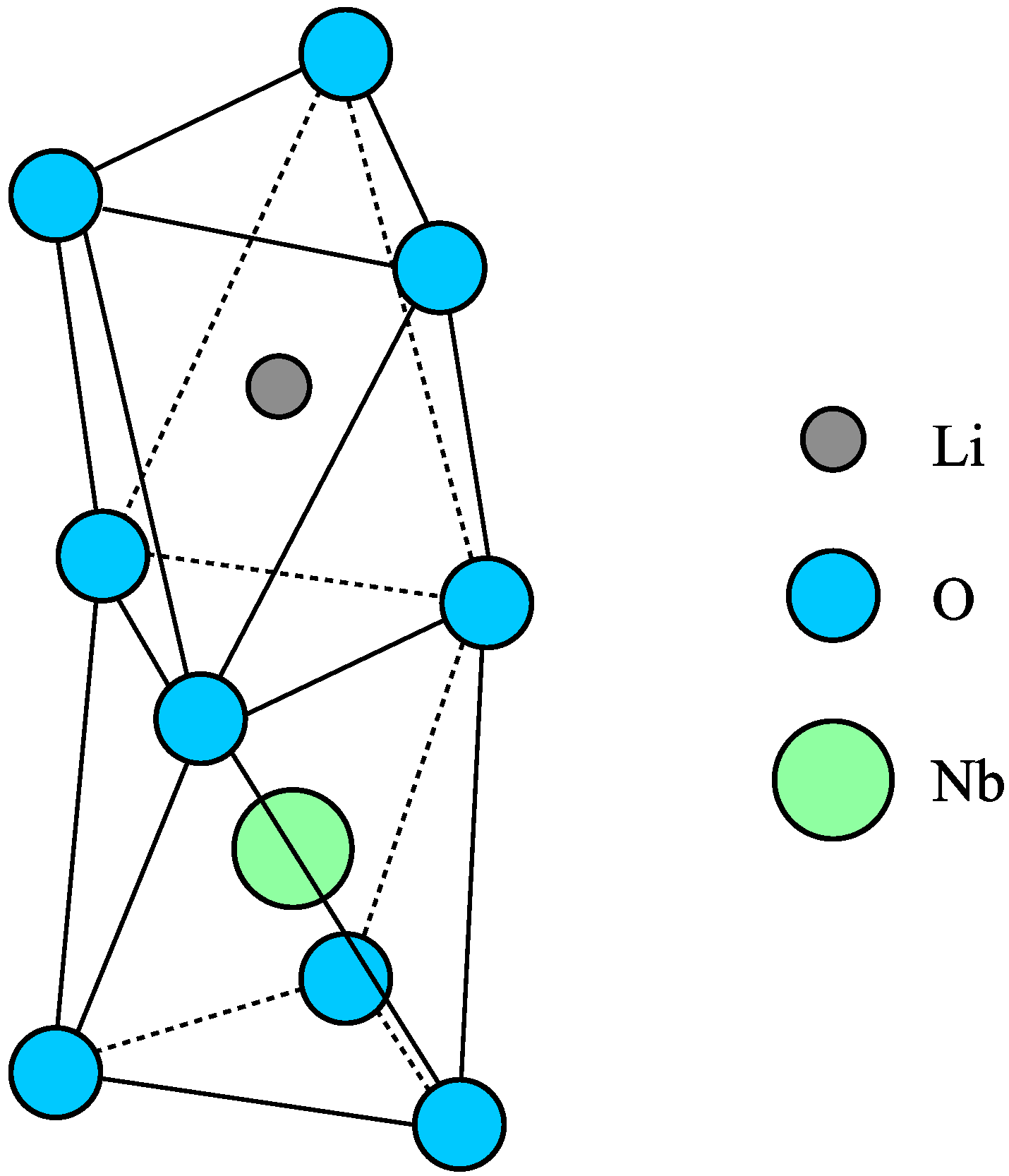
1. Introduction
2. Sputtering of LiNbO3: Principles and History
3. The Results of Sputtered TFLN Studies
4. Comparing Sputtering Methods with Other Epitaxy Methods
5. Conclusions
Author Contributions
Funding
Conflicts of Interest
References
- Boyd, G.D.; Miller, R.C.; Nassau, K.; Bond, W.L.; Savage, A. LiNbO3: An efficient phase matchable nonlinear optical material. Appl. Phys. Lett. 1964, 5, 234–236. [Google Scholar] [CrossRef]
- Matthias, B.T.; Remeika, J.P. Ferroelectricity in the ilmenite structure. Phys. Rev. 1949, 76, 1886. [Google Scholar] [CrossRef]
- Ballman, A.A. Growth of piezoelectric and ferroelectric materials by the CzochraIski technique. J. Am. Ceram. Soc. 1965, 48, 112–113. [Google Scholar] [CrossRef]
- Turner, E.H. High-frequency electro-optic coefficients of lithium niobate. Appl. Phys. Lett. 1966, 8, 303–304. [Google Scholar] [CrossRef]
- Kaminow, I.P.; Johnston, W.D. Quantitative determination of sources of the electro-optic effect in LiNbO3 and LiTaO3. Phys. Rev. 1967, 160, 519. [Google Scholar] [CrossRef]
- Subbarao, E.C. Ferroelectric and antiferroelectric materials. Ferroelectrics 1973, 5, 267–280. [Google Scholar] [CrossRef]
- Wemple, S.H.; DiDomenico, M.; Camlibel, I. Relationship between linear and quadratic electro-optic coefficients in LiNbO3, LiTaO3, and other oxygen-octahedra ferroelectrics based on direct measurement of spontaneous polarization. Appl. Phys. Lett. 1968, 12, 209–211. [Google Scholar] [CrossRef]
- Yamada, T.; Niizeki, N.; Toyoda, H. Piezoelectric and elastic properties of lithium niobate single crystals. Jpn. J. Appl. Phys. 1967, 6, 151. [Google Scholar] [CrossRef]
- Clark, M.G.; DiSalvo, F.J.; Glass, A.M.; Peterson, G.E. Electronic structure and optical index damage of iron-doped lithium niobate. J. Chem. Phys. 1973, 59, 6209–6219. [Google Scholar] [CrossRef]
- Amodei, J.J.; Staebler, D.L. Holographic recording in lithium niobate. RCA Rev. 1972, 33, 71–93. [Google Scholar]
- Weis, R.S.; Gaylord, T.K. Lithium niobate: Summary of physical properties and crystal structure. Appl. Phys. A 1985, 37, 191–203. [Google Scholar] [CrossRef]
- Schröder, M.; Haußmann, A.; Thiessen, A.; Soergel, E.; Woike, T.; Eng, L.M. Conducting domain walls in lithium niobate single crystals. Adv. Funct. Mater. 2012, 22, 3936–3944. [Google Scholar] [CrossRef]
- Poberaj, G.; Hu, H.; Sohler, W.; Guenter, P. Lithium niobate on insulator for micro-photonic devices. Laser Photonics Rev. 2012, 6, 488–503. [Google Scholar] [CrossRef]
- Sarabalis, C.J.; McKenna, T.P.; Patel, R.N.; Laer, R.; Naeini, A.H. Acousto-optic modulation in lithium niobate on sapphire. APL Photonics 2020, 5, 086104. [Google Scholar] [CrossRef]
- Cecelja, F.; Bordovsky, M.; Balachandran, W. Lithium niobate sensor for measurement of DC electric fields. IEEE Trans. Instrum. Meas. 2001, 50, 465–469. [Google Scholar] [CrossRef]
- Wooten, E.L.; Kissa, K.M.; Yan, A.; Murphy, E.J.; Lafaw, D.A.; Hallemeier, P.F.; Maack, D.; Attanasio, D.V.; Fritz, D.J.; McBrien, G.J.; et al. A review of lithium niobate modulators for fiber-optic communications systems. IEEE J. Sel. Top. Quantum Electron. 2000, 6, 69–82. [Google Scholar] [CrossRef]
- Lim, E.J.; Fejer, M.M.; Byer, R.L. Second harmornic generation of green light in periodically poled planar LiNbO3 waveguide. Electron. Lett. 1989, 3, 174–175. [Google Scholar] [CrossRef]
- Sulser, F.; Poberaj, G.; Koechlin, M.; Günter, P. Photonic crystal structures in ion-sliced lithium niobate thin films. Opt. Express 2009, 17, 020291. [Google Scholar] [CrossRef]
- Sumets, M.P.; Dybov, V.A.; Ievlev, V.M. LiNbO3 films: Potential application, synthesis techniques, structure, properties. Inorg. Mater. 2017, 53, 1361–1377. [Google Scholar] [CrossRef]
- Zeng, X.; Pelenovich, V.; Xu, C.; Neena, D.; Jiang, Y.; Zhang, X.; Porgrebnyak, A.; Rakhimov, R.; Zhang, J.; Yang, B.; et al. Morphology of lithium niobium oxide thin film ultrasonic transducers deposited by RF magnetron sputtering. Ceram. Int. 2023, 49, 16297–16304. [Google Scholar] [CrossRef]
- Lo Presti, F.; Pellegrino, A.L.; Micard, Q.; Condorelli, G.G.; Margueron, S.; Bartasyte, A.; Malandrino, G. LiNbO3 thin films through a sol–gel/spin-coating approach using a novel heterobimetallic lithium–niobium precursor. Nanomaterials 2024, 14, 345. [Google Scholar] [CrossRef] [PubMed]
- Sauze, L.C.; Vaxelaire, N.; Templier, R.; Rouchon, D.; Pierre, F.; Guedj, C.; Remiens, D.; Rodriguez, G.; Bousquet, M.; Dupont, F. Homo-epitaxial growth of LiNbO3 thin films by Pulsed Laser deposition. J. Cryst. Growth 2023, 601, 126950. [Google Scholar] [CrossRef]
- Pellegrino, A.L.; Wagner, E.; Lo Presti, F.; Maudez, W.; Kolb, S.; Rani, R.; Bernard, A.; Guy, S.; Gassenq, A.; Raevskaia, M.; et al. Efficient Optimization of High-Quality Epitaxial Lithium Niobate Thin Films by Chemical Beam Vapor Deposition: Impact of Cationic Stoichiometry. Adv. Mater. Interfaces 2023, 10, 2300535. [Google Scholar] [CrossRef]
- Lu, Y.; Dekker, P.; Dawes, J.M. Growth and characterization of lithium niobate planar waveguides by liquid phase epitaxy. J. Cryst. Growth 2009, 311, 1441–1445. [Google Scholar] [CrossRef]
- Tumanov, N.A.; Kirillov, D.V.; Vorob’ev, E.V. Investigation of a high-frequency magnetron sputtering system operation modes during copper thin films deposition. J. Phys. Conf. Ser. 2022, 2270, 012055. [Google Scholar] [CrossRef]
- Dybov, V.; Serikov, D.; Ryzhkova, G.; Sumets, M. Early stages of lithium niobate films growth fabricated by radio-frequency magnetron sputtering on crystalline (001) Si. Surf. Interfaces 2020, 19, 100530. [Google Scholar] [CrossRef]
- Sauze, L.C.; Vaxelaire, N.; Rouchon, D.; Pierre, F.; Templier, R.; Remiens, D.; Rodriguez, G. Microstructural and chemical analysis of polycrystalline LiNbO3 films obtained by room-temperature RF sputtering after various annealing durations. J. Vac. Sci. Technol. A 2020, 38, 043205. [Google Scholar] [CrossRef]
- Zivasatienraj, B.; Tellekamp, M.B.; Doolittle, W.A. Epitaxy of LiNbO3 historical challenges and recent success. Crystals 2021, 11, 397. [Google Scholar] [CrossRef]
- Takada, S.; Ohnishi, M.; Hayakawa, H.; Mikoshiba, N. Optical waveguides of single-crystal LiNbO3 film deposited by rf sputtering. Appl. Phys. Lett. 1974, 24, 490–492. [Google Scholar] [CrossRef]
- Hewig, G.M.; Jain, K.; Sequeda, F.O.; Tom, R.; Wang, P.W. RF Sputtering of LiNbO3 thin films. Thin Solid Film. 1982, 88, 67–74. [Google Scholar] [CrossRef]
- Kanata, T.; Kobayashi, Y.; Kubota, K. Epitaxial growth of LiNbO3-LiTaO3 thin films on Al2O3. J. Appl. Phys. 1987, 62, 2989–2993. [Google Scholar] [CrossRef]
- Lansiaux, X.; Dogheche, E.; Remiens, D.; Viry, M.; Perrin, A.; Ruterana, P. LiNbO3 thick films grown on sapphire by using a multistep sputtering process. J. Appl. Phys. 2001, 90, 5274–5277. [Google Scholar] [CrossRef]
- Lee, S.Y.; Route, R.K.; Feigelson, R.S. The Growth of Optical Quality LiNbO3 Thin Films On Sapphire and LiTao3 Substrates Using Solid-Source Mocvd. MRS Online Proc. Libr. 1995, 392, 177. [Google Scholar] [CrossRef]
- Feigelson, R.S. Epitaxial growth of lithium niobate thin films by the solid source MOCVD method. J. Cryst. Growth 1996, 166, 1–16. [Google Scholar] [CrossRef]
- Zhao, L.; Shi, L.; Wang, J.; Yan, J.; Chen, Y.; Zheng, Y. Effect of doping Mg on the structure and optical properties of LiNbO3 films prepared by radio-frequency magnetron sputtering. Mater. Sci. Semicond. Process. 2020, 108, 104901. [Google Scholar] [CrossRef]
- Sumets, M.; Ievlev, V.; Kostyuchenko, A.; Dybov, V.; Kotov, G.; Sidorkin, A. Charge phenomena at the Si/LiNbO3 heterointerface after thermal annealing. Ceram. Int. 2018, 44, 15058–15064. [Google Scholar] [CrossRef]
- Sumets, M. Charge transport in LiNbO3-based heterostructures. J. Nonlinear Opt. Phys. Mater. 2017, 26, 1750011. [Google Scholar] [CrossRef]
- McMillen, D.K.; Hudson, T.D.; Wagner, J.; Singleton, J.S.; Banerjee, P.P.; Danileiko, A.Y.; Yin, S.; Wang, Y.; Yu, F.T.S.; Darwish, A.M.; et al. Analysis of twelve specially doped lithium niobate crystals. In Proceedings of the Photorefractive Fiber and Crystal Devices: Materials, Optical Properties, and Applications III, San Diego, CA, USA, 22 September 1997. [Google Scholar] [CrossRef]
- Zhao, L.; Zhu, Y.; Yan, J.; Chen, Y. Effect of doping Zn on the optical and electrical properties of LiNbO3 films. Condens. Matter 2021, 611, 412981. [Google Scholar] [CrossRef]
- Wetzl, P.A. Iron-Doped Lithium Niobate Thin Films on GaN: Fabrication and Characterization. Master’s Thesis, University of Padua, Padua, Italy, 2021. [Google Scholar]
- Jiangou, Z.; Shipin, Z.; Dingquan, X.; Xiu, W.; Guanfeng, X. Optical absorption properties of doped lithium niobate crystals. Condens. Matter 1992, 4, 2977. [Google Scholar] [CrossRef]
- Chen, Z.; Xu, Q.; Zhang, K.; Wong, W.H.; Zhang, D.L.; Pun, E.Y.; Wang, C. Efficient erbium-doped thin-film lithium niobate waveguide amplifiers. Opt. Lett. 2021, 46, 1161–1164. [Google Scholar] [CrossRef]
- Saeed, S.; Liu, H.; Xue, L.; Zheng, D.; Liu, S.; Chen, S.; Kong, Y.; Rupp, R.; Xu, J. Enhancement of photorefraction in vanadium-doped lithium niobate through iron and zirconium co-doping. Materials 2019, 12, 3143. [Google Scholar] [CrossRef] [PubMed]
- Sidorov, N.V.; Shuvalova, A.M.; Yanichev, A.A.; Teplyakova, N.A.; Palatnikov, M.N.; Bormanis, K. Photoelectric fields in doped lithium niobate crystals. Integr. Ferroelectr. 2019, 196, 43–46. [Google Scholar] [CrossRef]
- Smith, F.W.; Ghidini, G. Reaction of oxygen with Si (111) and (100): Critical conditions for the growth of SiO2. J. Electrochem. Soc. 1982, 129, 1300. [Google Scholar] [CrossRef]
- Malitson, I.H. Interspecimen comparison of the refractive index of fused silica. JOSA 1965, 55, 1205–1209. [Google Scholar] [CrossRef]
- Huang, C.H.; Rabson, T.A. Low-loss thin-film LiNbO3 optical waveguide sputtered onto a SiO2/Si substrate. Opt. Lett. 1993, 18, 811–813. [Google Scholar] [CrossRef]
- Akazawa, H. Trials to achieve high-quality c-axis-oriented LiNbO3 thin films: Sputter-deposition on a-SiO2, ZnO/SiO2, quartz (0001), and SrTiO3 (111) substrates. Thin Solid Film. 2022, 748, 139148. [Google Scholar] [CrossRef]
- Malitson, I.H. Refraction and dispersion of synthetic sapphire. J. Opt. Soc. Am. 1962, 52, 1377–1379. [Google Scholar] [CrossRef]
- Dogheche, E.H.; Lansiaux, X.; Remiens, D. Growth and optical waveguiding properties of rf sputtered lithium niobate thin films on sapphire substrates. Integr. Ferroelectr. 1999, 25, 47–59. [Google Scholar] [CrossRef]
- Shimizu, M.; Furushima, Y.; Nishida, T.N.; Shiosaki, T.S. Preparation and optical waveguide properties of LiNbO3 thin films by rf magnetron sputtering. Jpn. J. Appl. Phys. 1993, 32, 4111. [Google Scholar] [CrossRef]
- Tan, S.; Gilbert, T.; Hung, C.Y.; Schlesinger, T.E.; Migliuolo, M. Sputter deposited c-oriented LiNbO3 thin films on SiO2. J. Appl. Phys. 1996, 79, 3548–3553. [Google Scholar] [CrossRef]
- Tan, S.; Schlesinger, T.E.; Migliuolo, M. The role of Si3N4 layers in determining the texture of sputter deposited LiNbO3 thin films. Appl. Phys. Lett. 1996, 68, 2651–2653. [Google Scholar] [CrossRef]
- Shandilya, S.; Tomar, M.; Gupta, V. Deposition of stress free c-axis oriented LiNbO3 thin film grown on (002) ZnO coated Si substrate. J. Appl. Phys. 2012, 111, 102803. [Google Scholar] [CrossRef]
- Huang, C.J.; Chui, H.K.; Stone, B.A.; Rost, T.A.; Rabson, T.A. Optical characterization of lithium niobate thin films. In Proceedings of the IEEE 7th International Symposium on Applications of Ferroelectrics, Urbana, IL, USA, 6–8 June 1990. [Google Scholar] [CrossRef]
- Sauze, L.C.; Vaxelaire, N.; Rouchon, D.; Templier, R.; Remiens, D.; Rodriguez, G.; Dupont, F. Effect of the annealing treatment on the physical and structural properties of LiNbO3 thin films deposited by radio-frequency sputtering at room temperature. Thin Solid Film. 2021, 726, 138660. [Google Scholar] [CrossRef]
- Ballman, A.A.; Brown, H.; Tien, P.K.; Sanseverino, S. The growth of LiNbO3 thin films by liquid phase epitaxial techniques. J. Cryst. Growth 1975, 29, 289–295. [Google Scholar] [CrossRef]
- Tamada, H.; Yamada, A.; Saitoh, M. LiNbO3 thin-film optical waveguide grown by liquid phase epitaxy and its application to second-harmonic generation. J. Appl. Phys. 1991, 70, 2536–2541. [Google Scholar] [CrossRef]
- Yamada, A.; Tamada, H.; Saitoh, M. LiNbO3 thin-film optical waveguide grown by liquid phase epitaxy using Li2O-B2O3 flux. Appl. Phys. Lett. 1992, 61, 2848–2850. [Google Scholar] [CrossRef]
- Miyazawa, S.; Fushimi, S.; Kondo, S. Optical waveguide of LiNbO3 thin film grown by liquid phase epitaxy. Appl. Phys. Lett. 1975, 26, 8–10. [Google Scholar] [CrossRef]
- Curtis, B.J.; Brunner, H.R. The growth of thin films of lithium niobate by chemical vapour de position. Mater. Res. Bull. 1975, 10, 515–520. [Google Scholar] [CrossRef]
- Kilburger, S.; Millon, E.; Di Bin, P.; Boulle, A.; Guinebretière, R.; Di Bin, C. Properties of LiNbO3 based heterostructures grown by pulsed. Thin Solid Film. 2010, 518, 4654–4657. [Google Scholar] [CrossRef]
- Stankova, N.E.; Tonchev, S.H.; Gyorgy, E.; Socol, G.; Mihailescu, I. Pulsed laser deposition of LiNbO3 thin films from Li-rich targets. J. Optoelectron. Adv. Mater. 2004, 6, 1345–1348. [Google Scholar]
- Betts, R.A.; Pitt, C.W. Growth of thin-film lithium niobate by molecular beam epitaxy. Electron. Lett. 1985, 21, 960–962. [Google Scholar] [CrossRef]
- Jia, Y.; Wang, L.; Chen, F. Ion-cut lithium niobate on insulator technology: Recent advances and perspectives. Appl. Phys. Rev. 2021, 8, 011307. [Google Scholar] [CrossRef]
- Boes, A.; Corcoran, B.; Chang, L.; Bowers, J.; Mitchell, A. Status and potential of lithium niobate on insulator (LNOI) for photonic integrated circuits. Laser Photonics Rev. 2018, 12, 1700256. [Google Scholar] [CrossRef]
- Hu, H.; Yang, J.; Gui, L.; Sohler, W. Lithium niobate-on-insulator (LNOI): Status and perspectives. In Silicon Photonics and Photonic Integrated Circuits III; SPIE: Bellingham, WA, USA, 2012. [Google Scholar] [CrossRef]
- Krasnokutska, I.; Tambasco, J.L.; Li, X.; Peruzzo, A. Ultra-low loss photonic circuits in lithium niobate on insulator. Opt. Express 2018, 26, 897–904. [Google Scholar] [CrossRef]
- Scott, J.F. Status report on ferroelectric memory materials. Integr. Ferroelectr. 1998, 20, 15–23. [Google Scholar] [CrossRef]
- Sumets, M.; Ievlev, V.; Kostyuchenko, A.; Vakhtel, V.; Kannykin, S.; Kobzev, A. Electrical properties of Si–LiNbO3 heterostructures grown by radio-frequency magnetron sputtering in an Ar + O2 environment. Thin Solid Film. 2014, 552, 32–38. [Google Scholar] [CrossRef]
- Sumets, M.; Ievlev, V.; Kostyuchenko, A.; Kuzmina, V. Influence sputtering conditions on electrical characteristics of Si-LiNbO3 heterostructures formed by radio-frequency magnetron sputtering. Mol. Cryst. Liq. Cryst. 2014, 603, 202–215. [Google Scholar] [CrossRef]
- Ievlev, V.; Sumets, M.; Kostyuchenko, A.; Ovchinnikov, O.; Vakhtel, V.; Kannykin, S. Band diagram of the Si-LiNbO3 heterostructures grown by radio-frequency magnetron sputtering. Thin Solid Film. 2013, 542, 289–294. [Google Scholar] [CrossRef]
- Streque, J.; Aubert, T.; Kokanyan, N.; Bartoli, F.; Taguett, A.; Polewczyk, V.; Kokanyan, E.; Hage-Ali, S.; Boulet, P.; Elmazria, O. Stoichiometric lithium niobate crystals: Towards identifiable wireless surface acoustic wave sensors operable up to 600 °C. IEEE Sens. Lett. 2019, 3, 1–4. [Google Scholar] [CrossRef]
- Zhang, S.; Lu, R.; Zhou, H.; Link, S.; Yang, Y.; Li, Z.; Huang, K.; Ou, X.; Gong, S. Surface acoustic wave devices using lithium niobate on silicon carbide. IEEE Trans. Microw. Theory Tech. 2020, 68, 3653–3666. [Google Scholar] [CrossRef]
- Robinson, H.; Pitt, C.W.; Gibson, R.A. Silicon lithium niobate electro-optic waveguide modulator structures in the parallel-plate configuration. Appl. Opt. 1993, 32, 3981–3988. [Google Scholar] [CrossRef]
- Fukuzawa, H.; Yoshinari, J.; Hara, H.; Sasaki, K.; Take, H.; Yoshida, M.; Shimura, A.; Kikukawa, T. Visible light modulator by sputter-deposited lithium niobate. AIP Adv. 2022, 12, 065029. [Google Scholar] [CrossRef]
- Wang, C.; Zhang, M.; Chen, X.; Bertrand, M.; Shams-Ansari, A.; Chandrasekhar, S.; Winzer, P.; Lončar, M. Integrated lithium niobate electro-optic modulators operating at CMOS-compatible voltages. Nature 2018, 562, 101–104. [Google Scholar] [CrossRef] [PubMed]
- Hara, H.; Yoshinari, J.; Sasaki, K.; Kikukawa, T.; Take, H.; Mino, T.; Shimura, A.; Takagi, Y.; Fukuzawa, H. Low voltage visible light modulation for three colors (red, green, blue) by sputtered lithium niobate thin film. AIP Adv. 2024, 14, 015045. [Google Scholar] [CrossRef]
- Lee, T.H.; Hwang, F.T.; Lee, C.T.; Lee, H.Y. Investigation of LiNbO3 thin films grown on Si substrate using magnetron sputter. Mater. Sci. Eng. B 2007, 136, 92–95. [Google Scholar] [CrossRef]
- Tada, H.; Kumpel, A.E.; Lathrop, R.E.; Slanina, J.B.; Nieva, P.; Zavracky, P.; Miaoulis, I.N.; Wong, P.Y. Thermal expansion coefficient of polycrystalline silicon and silicon dioxide thin films at high temperatures. J. Appl. Phys. 2000, 87, 4189–4193. [Google Scholar] [CrossRef]
- Kim, Y.S.; Smith, R.T. Thermal expansion of lithium tantalate and lithium niobate single crystals. J. Appl. Phys. 1969, 40, 4637–4641. [Google Scholar] [CrossRef]


| Reference | Substrate | RF Power | Target Diameter | Ar/O2 Ratio | Spacing | Gas Pressure | Temperature | TFLN Phase |
|---|---|---|---|---|---|---|---|---|
| [47] | Si(100)/SiO2 | 50 W | 7.62 cm | 60/40 | 5 cm | 2–5 mTorr | 500–600 °C | (104) |
| [29] | Al2O3 | 50 W | 9 cm | 60/40 | 4 cm | 200 mTorr | 500 °C | - |
| [50] | Al2O3 (001) | 180 W | 7.62 cm | 60/40 | 6 cm | 20 mTorr | 500 °C | (006) |
| [51] | Al2O3 (001) | 50–200 W | - | 80/20–60/40 | - | 5–80 mTorr | 600 °C | (001) |
| [51] | Al2O3 (110) | 50–200 W | - | 80/20–60/40 | - | 5–80 mTorr | 400 °C | (110) |
| [51] | Al2O3 (110) | 50–200 W | - | 80/20–60/40 | - | 5–80 mTorr | 600 °C | (110) |
| [52] | Si/SiO2 (1.2 μm) | 1 W/cm2 | - | - | - | - | 500–600 °C, no annealing | (012), (110), (006) |
| [52] | Si/SiO2 (1.2 μm) | 1 W/cm2 | - | - | - | - | 500–600 °C, annealed at 750 °C | (012) + peak at 2Θ = 29° |
| [52] | Si/SiO2 (1.2 μm)/Si3N4 (200 nm) | 1 W/cm2 | - | - | - | - | 500–600 °C | (006) + LiNb3O8 |
| [52] | Si | 25 W | 5.08 cm | 60/40 | - | 5 mTorr | 530 °C | (006) |
| [54] | Si/Zno (002) | 75 W | 10.16 cm | 70/30 | 7.5 cm | 8–14 mTorr | 450 °C | 2Θ = 38.21° |
| [55] | Al2O3 (110) | 150 W | - | 60/40 | 6 cm | 6 mTorr | 580 °C | (110) |
| [55] | Al2O3 (001) | 150 W | - | 60/40 | 6 cm | 6 mTorr | 580 °C | (110), (006) |
| Method | Optical Loss, dB/cm | Film Thickness, nm | Substrate | Note | Reference |
|---|---|---|---|---|---|
| LPE | 1–5 | 3000 | LiTaO3 | - | [57] |
| 25 | 3640 | LiTaO3 | - | [58] | |
| <1 | 10,000 | MgO-doped Z-plate LiNbO3 | λ = 458 nm | [59] | |
| 5 | 3000 | c-oriented LiTaO3 | TM-mode λ = 458 nm | [60] | |
| 11 | c-oriented LiTaO3 | TE-mode, λ = 458 nm | |||
| CVD | 2 | 120 | C-plate Al2O3 | - | [33,34] |
| 6 | 500 | Z-cut LiTaO3 | - | ||
| 40 | 300 | LiTaO3 () | - | [61] | |
| PLD | <1.5 | 140 | Al2O3 (001) | - | [62] |
| 18 | 260 | Al2O3 (001) substrate | λ = 632.8 nm | [63] | |
| MBE | 15.7 | 50 | Al2O3 | [64] | |
| Sputtering | 9 | 180 | Al2O3 | [29] | |
| 1.2 | 630 | Al2O3 (001) | λ = 632.8 nm, TE0 | [32] | |
| 1.2 | 600 | Al2O3 (001), (110) | λ = 632.8 nm | [55] | |
| 21.9 | - | ZnO | - | [51] | |
| 19.8 | - | Corning 7059 | Before annealing | ||
| 9.13 | - | Corning 7059 | After annealing | ||
| 27.5 | - | Al2O3 (110) | Before annealing | ||
| 25.6 | - | Al2O3 (110) | After annealing | ||
| 40.2 | - | Al2O3 (001) | - |
Disclaimer/Publisher’s Note: The statements, opinions and data contained in all publications are solely those of the individual author(s) and contributor(s) and not of MDPI and/or the editor(s). MDPI and/or the editor(s) disclaim responsibility for any injury to people or property resulting from any ideas, methods, instructions or products referred to in the content. |
© 2025 by the authors. Licensee MDPI, Basel, Switzerland. This article is an open access article distributed under the terms and conditions of the Creative Commons Attribution (CC BY) license (https://creativecommons.org/licenses/by/4.0/).
Share and Cite
Kuznetsov, I.; Perin, A.; Gulyaeva, A.; Krutov, V. Sputtered LiNbO3 Thin Films for Application in Integrated Photonics: A Review. Crystals 2025, 15, 270. https://doi.org/10.3390/cryst15030270
Kuznetsov I, Perin A, Gulyaeva A, Krutov V. Sputtered LiNbO3 Thin Films for Application in Integrated Photonics: A Review. Crystals. 2025; 15(3):270. https://doi.org/10.3390/cryst15030270
Chicago/Turabian StyleKuznetsov, Igor, Anton Perin, Angelina Gulyaeva, and Vladimir Krutov. 2025. "Sputtered LiNbO3 Thin Films for Application in Integrated Photonics: A Review" Crystals 15, no. 3: 270. https://doi.org/10.3390/cryst15030270
APA StyleKuznetsov, I., Perin, A., Gulyaeva, A., & Krutov, V. (2025). Sputtered LiNbO3 Thin Films for Application in Integrated Photonics: A Review. Crystals, 15(3), 270. https://doi.org/10.3390/cryst15030270