Abstract
Methylammonium lead iodide (MAPbI3) perovskite has been widely studied for its optoelectronic properties, but its polycrystalline thin films inevitably contain grain boundaries and defects that degrade performance and stability. PbI2 is often considered a destabilizing agent in perovskites, yet it has also been reported to act as a passivation agent, making its role a subject of debate. Here, we performed integrated optical, photoluminescence (PL), and ultra-low-frequency Raman mapping on a 100 μm2 region of MAPbI3 thin films to study the roles of PbI2. The analyses resolved α-phase MAPbI3-rich, PbI2-rich, and mixed-phase domains, revealing heterogeneous PbI2 distribution with PL quenching at defect sites. In addition, after light-induced degradation, PL changes were governed by both the local microstructure and PbI2 distribution. Notably, PbI2-rich regions retained PL, evidencing a protective passivation effect. These findings demonstrate that the beneficial role of PbI2 is key to designing more stable perovskite devices.
1. Introduction
Hybrid organic-inorganic halide perovskites (HOIPs) exhibit a set of outstanding optoelectronic properties. Owing to these advantages, HOIPs have been extensively employed in diverse optoelectronic devices [1,2,3]. Among various halide perovskites, methylammonium lead iodide (MAPbI3) has been studied as one of the most representative materials for optoelectronic applications. MAPbI3 possesses a direct bandgap of 1.57 eV [4], which can be readily tuned by halide substitution or halide mixing [5]. Its exciton binding energy (37–50 meV) is comparable to or smaller than the thermal energy at room temperature (~25 meV), enabling efficient exciton dissociation under ambient conditions [6,7,8]. Moreover, the fabrication process for MAPbI3 is relatively simple and cost-effective compared to other semiconductors [9,10].
However, MAPbI3 thin films are intrinsically polycrystalline [11], which introduces performance degradation associated with grain boundaries and related defects. Traps and non-radiative recombination centers—originating from chemical impurities or structural defects—are primary factors that limit device efficiency [5,12]. In particular, structural defects can act as Shockley-Read-Hall recombination centers, reducing carrier lifetimes and lowering the open-circuit voltage [13,14], and initiating progressive degradation when subjected to extreme operation conditions such as high temperature during laser lasing processes [15]. These defects can also accelerate environmental instability by increasing susceptibility to moisture and light [16]. Although MAPbI3 has been reported to show some tolerance to defects, they remain a main limitation for the performance of perovskite-based devices [17].
Additives such as PbI2 [18,19,20,21], phenethylammonium iodide [11,16,22], and dibenzopentacene (C64H36) [23] have been reported to suppress defects. Among them, PbI2 has been considered a destabilizing agent in perovskites, yet recently been reported to act as a passivation agent, thus leaving its role controversial.
A variety of characterization techniques have been utilized to clarify the passivation role of PbI2 distributed on a thin film [18]. Techniques such as scanning electron microscopy (SEM), atomic force microscopy (AFM), and mapping mode energy dispersive X-ray spectroscopy provide spatial information, but integrated multimodal mapping on identical sample locations remains uncommon.
In this regard, ultra-low frequency Raman (<100 cm−1) is highly advantageous, as it allows direct discrimination between PbI2 and α-phase MAPbI3, making it an ideal tool for addressing the debated role of PbI2 in thin films [24,25,26,27,28,29,30].
In this work, we demonstrate that the debated role of PbI2 in MAPbI3 thin films can be clarified through integrated spatially resolved optical, PL, and Raman mapping for a 100 μm2 area. This approach revealed heterogeneous PbI2 distributions and the emergence of persistent PbI2-passivated microdomains that retain PL even under degradation conditions. These findings demonstrate that the beneficial role of PbI2 is key to designing more stable perovskite devices.
2. Materials and Methods
2.1. Perovskite Thin Film Preparation
PbI2 was purchased from TCI (Tokyo, Japan) and used as received. All other chemicals were obtained from Sigma-Aldrich (Darmstadt, Germany) and also used as received.
MAPbI3 perovskite thin films were fabricated via an anti-solvent-assisted spin-coating method, with methylammonium chloride (MACl) as an additive to stabilize the intermediate phase and improve crystallographic orientation. MACl largely evaporates during annealing and does not disturb the intrinsic structure [31]. Glass substrates were pretreated with oxygen plasma before film deposition.
The precursor solution was prepared by dissolving 1.53 M PbI2, 1.40 M methylammonium iodide (MAI), and 0.50 M MACl in a mixed solvent of DMF and DMSO (DMF:DMSO = 8:1, v/v). The solution was stirred continuously at 70 °C for 6 h. For film preparation, the precursor solution was spin-coated on the ozone-etched glass substrate in two steps, which was secured on the spin-coater (EF-4op, E-flex, Bucheon, Republic of Korea), using a micropipette: 1000 rpm for 10 s, followed by 4000 rpm for 30 s. During the second step, 200 μL of diethyl ether was dripped onto the spinning substrate 10 s after the start of the second step. The films were then annealed at 120 °C for 60 min in a nitrogen atmosphere. After annealing, the sample was allowed to cool to room temperature inside the glovebox before characterization. The film thickness was approximately 250 nm. The overall fabrication process is schematically illustrated in Figure 1.
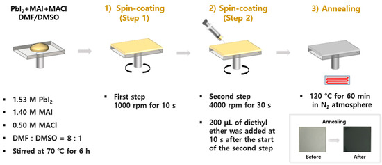
Figure 1.
Schematic illustration of the perovskite thin film fabrication process via the anti-solvent-assisted spin-coating method.
2.2. Optical Characterization
X-ray diffraction (XRD) patterns were recorded using a powder diffractometer (X’Pert3, PANalytical, Almelo, The Netherlands) equipped with Cu Kα radiation (λ = 1.54 Å). UV-Vis absorption spectra were acquired with a spectrophotometer (V-770, JASCO, Tokyo, Japan).
Raman and PL mapping were performed using a confocal Raman microscope (LabRAM HR Evolution, Horiba Jobin-Yvon, Palaiseau, France) equipped with an Olympus SMPLN 100× objective lens. A 633 nm He-Ne laser was used as the excitation source for both Raman and PL measurements. The laser spot diameter at the sample surface was ~0.86 μm. For PL mapping, the laser power was reduced to 0.0137 W cm−2@633 nm, and the integration time was set to 0.05 s per point to minimize photodegradation. For Raman measurements, Raman pump power was reduced to 12 W cm−2@633 nm, with an integration time of 30 s. All spatially resolved measurements were conducted over a 10 μm × 10 μm area with a step size of 1 μm.
3. Results and Discussion
3.1. Optical and Structural Characterization of MAPbI3 Thin Films
The UV-Vis absorption and steady-state PL spectra of the MAPbI3 perovskite thin film were measured at room temperature. As shown in Figure 2a, the emission peak is centered near 780 nm, closely matching the absorption onset, and the absorption spectrum extends across most of the visible range, together indicating the successful formation of the MAPbI3 perovskite thin film on the substrate [32]. This emission is consistent with the tetragonal phase of MAPbI3, which has a band gap of approximately 1.60 eV (corresponding to PL near 775 nm); the observed ~5 nm redshift may arise from slight variations in film quality or measurement conditions [33]. The X-ray diffraction (Figure 2b) further supports the formation of the MAPbI3 perovskite phase, showing distinct peaks at 14.08° (110), 28.5° (220), and 32° (310), characteristic of the tetragonal crystal phase (space group I4/mcm) [5,12,32].
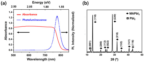
Figure 2.
(a) UV-Vis absorption and normalized steady-state photoluminescence (PL) spectra, and (b) X-ray diffraction (XRD) patterns of methylammonium lead iodide (MAPbI3) perovskite thin film. Diffraction peaks corresponding to PbI2 and MAPbI3 are marked by ☐ and ◆, respectively.
A minor peak at 12.6°, attributed to the (001) plane of lead iodide [34], was also observed, indicating the presence of a small amount of lead iodide, presumed to originate either from incomplete conversion of the PbI2 precursor during crystallization or from the degradation of the perovskite thin film after synthesis. Because MAPbI3 has a low formation enthalpy, it is prone to degradation into PbI2 and volatile MAI [16]. Thus, these diffraction results suggest that the fabricated film predominantly consists of the α-phase MAPbI3, with a small amount of PbI2.
3.2. Correlation Analysis of Optical Microscopy and Spatially Resolved PL Mapping
To spatially investigate the structural heterogeneity of the polycrystalline MAPbI3 perovskite thin film, optical microscopy and microscale PL mapping were acquired from the same region of the film to allow direct spatial correlation between morphological and photoluminescence features. Figure 3a,b present an optical microscope image and the corresponding PL intensity contour map, respectively, focusing on a surface defect and its surrounding region. The optical microscope image in Figure 3a clearly reveals pronounced surface defects localized at the junctions. Due to the inherent polycrystalline nature of MAPbI3, grain boundaries are commonly formed [16]. Since individual grains of MAPbI3 thin films can typically be identified at SEM-level resolution, the fracture observed in Figure 3a is more likely a relatively large crack, which is often associated with the film processing steps, rather than a typical grain boundary. Nevertheless, because the internal width of this crack is only ~2 μm at most, there is a possibility that it might be overlooked even at a resolution of about 1 μm in Raman mapping that covers larger areas [35]. Similar to typical grain boundaries, these defects can hinder charge carrier transport and often serve as sites for further defect formation [16]. The PL contour map in Figure 3b exhibits a clear spatial correlation with the optical features. For instance, region A, which appears relatively smooth in the optical image, shows the strongest PL emission, while region C, associated with defective regions, displays the weakest and most redshifted PL signal (Figure 3c). This correlation suggests that the optical response, including both PL intensity and spectral position, is strongly influenced by surface morphology and the local defect environment exemplified by cracks. The reduced PL intensity and redshift near defect sites can be attributed to enhanced nonradiative recombination and possible bandgap reduction due to compositional variations or strain [36].
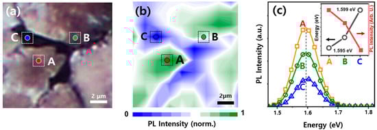
Figure 3.
(a) Optical image of MAPbI3 thin film, (b) PL intensity map acquired from the same area as shown in (a), and (c) representative PL spectra measured at spots A, B and C. The inset presents a comparison of the PL intensities(a.u., red line) and the corresponding optical bandgap values (eV, black line) for each of the three spots (A, B, and C).
3.3. Spatially Resolved Raman Mapping of Composition Distribution in Thin Films
To further investigate chemical information in the regions analyzed in Figure 3, Raman mapping was conducted on the same areas of the MAPbI3 perovskite thin film previously examined by optical and PL measurements. Figure 4a shows ultra-low frequency Raman spectra (40–200 cm−1) measured at three representative spots (A, B, and C) marked in Figure 3. Notably, no Raman feature near 143 cm−1, typically attributed to PbO vibrational modes, was detected in any region [37]. This absence indicates that the PL and Raman measurements employed here did not induce photodegradation under our experimental conditions [12,27].
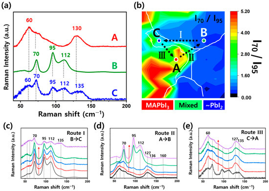
Figure 4.
(a) Ultra-low frequency Raman spectra (40−200 cm−1) measured at the representative points A−C shown in Figure 3, corresponding to α-phase MAPbI3-rich (A), PbI2-rich (B), and mixed-phase (C). (b) Raman intensity ratio (I70/I95) map with white line boundaries defined from the optical image, showing the distribution of chemical species. (c) Raman spectra along the dashed arrows in Route Ⅰ (B → C), (d) Route Ⅱ (A → B), and (e) Route Ⅲ (C → A).
Spots A and B, located on different grains, exhibit distinct Raman signatures. Spot A shows peak at 60 cm−1, assigned to the I-Pb-I bending mode in MAPbI3, which is a significant marker of its α-phase inorganic component [38]. A second peak at ~135 cm−1 is assigned to a librational mode of the MA cation confined within the inorganic cage of the perovskite lattice, consistent with previous reports [39]. The Raman features of α-phase MAPbI3 were clearly distinguished from those of MAI (see Figure S1) [40]. In contrast, spot B displays the peaks at 70 and 95 cm−1, characteristic of crystalline PbI2 and associated with the symmetric and asymmetric stretching vibrations of Pb–I bonds in edge-sharing PbI6 octahedra [38,41]. It shows good agreement with the Raman of PbI2 (see Figure S1) [42]. The Raman spectrum at spot C, located at the defect region, exhibits mixed features observed at spots A and B, indicating the coexistence of both α-phase MAPbI3 and PbI2. This implies that the defect contains residual PbI2 precursors or PbI2 formed by degradation. If excess PbI2 is present during the annealing process, it can be driven toward grain boundaries by perovskite grain growth, leading to its accumulation near defect sites [18,19].
With the incorporation of MACl additive, incomplete conversion thermodynamically results in residual PbI2 in the film. The PbI2 observed at spot C can be explained by its migration during annealing, while the strong signal at spot B likely arises from the same mechanism, leading to accumulation at grain boundaries or point defects beyond the current optical resolution [18]. This indicates that PbI2 is not uniformly distributed but accumulates locally within the film. Therefore, in spatially resolved analyses of MAPbI3 thin films using optical techniques such as Raman mapping, both structural defects (e.g., cracks) and the heterogeneous distribution of residual PbI2 must be carefully considered. Figure 4b presents a relative ratio map of the Raman peak intensities at 70 and 95 cm−1 (I70/I95) to distinguish the chemical species. As shown in Figure 4a, the peak at 70 cm−1 originates from crystalline PbI2, while the 95 cm−1 peak becomes dominant in PbI2-rich regions. Accordingly, higher I70/I95 ratios correspond to α-phase MAPbI3-rich domains, whereas lower ratios mark PbI2-rich domains. Figure 4c–e show the Raman spectra along the paths connecting the three points. The spectral changes occur abruptly, rather than gradually, upon crossing the interfaces between regions, consistent with the boundaries between compositionally distinct domains.
3.4. Integrated Multimodal Analysis at Identical Surface Locations
To provide a comprehensive comparison, the optical, PL, and Raman map data corresponding to the same region of the film were combined (Figure 5). It is evident that structural degradation is clearly correlated with the reduced PL intensity in the dark region (Figure 5a,b). These defect regions contain some PbI2 showing mixed Raman features (Figure 5c). Thus, the reduced PL is more reasonably explained by the presence of structural defects, such as cracks or voids, which increase non-radiative recombination rates. However, PbI2-rich regions can also emit bright PL comparable to that of α-phase MAPbI3-rich areas. The PL emission of pristine PbI2 powder or crystals deposited on a substrate, occurring at 2.50–2.43 eV, is distinct from the PL peak in this study and thus cannot account for the observed emission. Although PbI2 in coordinating solvents such as DMSO or DMF can form emissive polyiodide plumbate complexes. However, this emission is unlikely to be retained in a thin film due to the evaporation of the solvents during annealing [34,43]. To visualize the correlation between α-phase MAPbI3-rich and PbI2-rich regions on the Raman map and the PL intensity, we constructed a heat map by multiplying the PL and Raman signal values obtained at each spot (see Figure S2). Because higher PL intensity can be found in both pure α-phase MAPbI3-rich and PbI2-rich domains, Raman intensities were assigned negative values for PbI2-rich domains and positive values for MAPbI3-rich domains during the normalization of PL and Raman maps. Figure S2 demonstrates that blue regions represent negative correlation (i.e., strong PL associated with PbI2-rich domains) while red regions indicate positive correlation (i.e., strong PL associated with α-phase MAPbI3 domains). This analysis confirms that the PL intensity is correlated with both PbI2- and MAPbI3-rich regions.
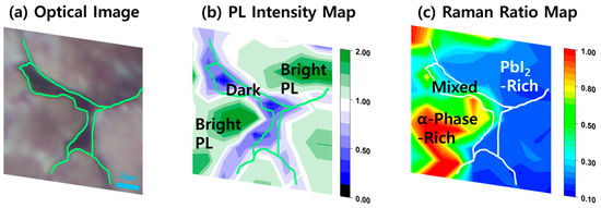
Figure 5.
Comparison of (a) optical image, (b) PL intensity map, and (c) Raman intensity ratio (I70/I95) map, reproduced from Figure 3a, Figure 3b, and Figure 4b, respectively. All images correspond to the same region of the film, enabling direct correlation of morphology, PL response, and phase distributions.
PbI2 has been reported to passivate MAPbI3, showing the reduction in defect density and suppression of degradation initiated at surface defects [23]. If the PbI2-rich regions observed in Figure 5c indeed reflect PbI2 concentrated at grain boundaries or local surface defects, it is plausible that PbI2 acts as a protective barrier against environmental degradation-inducing factors such as moisture, oxygen, or light, thereby mitigating further deterioration of the perovskite thin film.
3.5. Spatially Dependent Response of Thin Films to Light-Induced Degradation
To examine the passivation effect on the PL of MAPbI3 thin film, the sample was irradiated with an intense laser (120 W cm−2 @633 nm) under ambient conditions. The irradiation power is approximately 1200 times higher than the standard one-sun illumination (100 mW cm−2, AM 1.5G) [23].
The PL intensity and the red-shift magnitude maps were obtained (Figure 6a,b) after the irradiation. The α-phase MAPbI3 (A) and defect (C) regions exhibited no detectable PL after the irradiation, indicating photo-bleaching (③ in Figure 6c). In contrast, the PbI2-rich region (B) exhibited a slight red-shift upon irradiation yet retained a detectable PL signal (② in Figure 6c), indicating that the presence of PbI2 contributes to preserving the PL of the MAPbI3 thin film [20]. Although previous studies have reported that excessive PbI2, under specific conditions [18,44,45] such as light-induced decomposition or electric poling, increase the defect density of the film, our measurements indicate that the dominant effect of PbI2 is more consistent with passivation. Accordingly, the preserved PL emission in region (B) can originate from partial protection by PbI2 against irradiation-induced degradation.
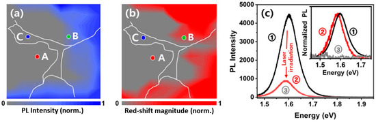
Figure 6.
(a) Normalized PL intensity and (b) red-shift magnitude heatmaps after intense irradiation. (c) Representative PL spectra before and after laser irradiation. Spectrum ① corresponds to the PL from spot B before irradiation, while spectra ② and ③ represent the PL from spots B and A after irradiation, respectively. The inset shows normalized PL spectra.
The influence of PbI2 on the performance and stability of MAPbI3 thin films remains debated, with both beneficial and detrimental effects reported [46,47,48,49,50]. Previous studies have addressed this issue either at the grain level using SEM or at broader scales using Raman mapping, often leading to ambiguous interpretations [18,35]. In contrast, our study demonstrates at an intermediate scale (10 μm × 10 μm) that PbI2 mitigates light-induced degradation, and that PL changes after irradiation are jointly governed by the local PbI2 distribution and the microstructure of MAPbI3 thin films.
4. Conclusions
In summary, we integrated optical, PL, and Raman mapping on identical surface regions of MAPbI3 thin films within a 10 μm × 10 μm field of view, enabling precise spatial correlation between local morphology and composition. Through this analytical approach, we observed that PbI2-rich microdomains retained PL even under light-induced degradation. These results highlight the critical role of spatially resolved, multimodal characterization in elucidating passivation mechanisms in polycrystalline perovskites.
This capability to perform multimodal measurements at the same location before and after light-induced degradation distinguishes our method from conventional techniques that either focus on highly localized features at high magnification (e.g., SEM and AFM) or characterize the entire film at low magnification. Accordingly, we anticipate that this nondestructive approach will serve as a powerful platform for preliminary evaluation of passivation strategies, including screening of passivation agents and their loading amounts, prior to more detailed characterization.
Supplementary Materials
The following supporting information can be downloaded at: https://www.mdpi.com/article/10.3390/cryst15110991/s1, Figure S1: Ultra-low Raman spectra of MAI and PbI2, Figure S2: PL–Raman correlation map. Red: PL–MAPbI3 correlation; Blue: PL–PbI2 correlation.
Author Contributions
Conceptualization, B.-G.K. and M.P.; Methodology, B.-G.K., J.C., T.S., and M.P.; Software, J.C.; Validation, B.-G.K., J.C., T.S., H.S.K., M.K., and J.J.; Formal Analysis, B.-G.K., J.C., and T.S.; Investigation, B.-G.K., J.C., T.S., and S.L.; Resources, M.K. and S.L.; Data Curation, H.S.K., M.K., J.J., and S.L.; Writing—Original Draft, B.-G.K., J.C., T.S., S.L., and M.P.; Writing—Review and Editing, J.C., T.S., H.S.K., M.K., J.J., S.L., and M.P.; Visualization, T.S., H.S.K., M.K., J.J., and M.P.; Supervision, S.L. and M.P.; Project Administration, S.L. and M.P.; Funding Acquisition, J.J., S.L., and M.P. All authors have read and agreed to the published version of the manuscript.
Funding
This research was supported by the Global—Learning & Academic research institution for Master’s·PhD students, and Postdocs(LAMP) Program of the National Research Foundation of Korea (NRF) grant funded by the Ministry of Education (No. RS-2023-00301702). This work was also supported by an NRF grant funded by the Korean government (MSIT) (RS-2023-00220748).
Data Availability Statement
The original contributions presented in this study are included in the article/Supplementary Materials. Further inquiries can be directed to the corresponding authors.
Conflicts of Interest
The authors declare no conflicts of interest.
References
- Heo, J.; Kim, H.; Park, J.; Sasongko, N.A.; Jeong, M.; Han, J.; Seo, T.; Ji, Y.; Han, J.; Park, M. Long-Term Comparisons of Photoluminescence Affected by Organic Cations of Formamidinium and Methylammonium in Monophasic Lead Iodide Perovskite Quantum Dots. Chem. Asian J. 2024, 19, e202400347. [Google Scholar] [CrossRef] [PubMed]
- Sasongko, N.A.; Jeong, Y.; Paramita, S.A.; Heo, J.; Oh, M.H.; Reyes-Lillo, S.E.; Park, M. Role of Size and Shape in Photoluminescence and Ultra-Low-Frequency Raman of Methylammonium Lead Iodide Perovskite Quantum Dots. J. Phys. Chem. Lett. 2025, 16, 1522–1528. [Google Scholar] [CrossRef]
- Chen, D.Q.; Chen, X. Luminescent perovskite quantum dots: Synthesis, microstructures, optical properties and applications. J. Mater. Chem. C 2019, 7, 1413–1446. [Google Scholar] [CrossRef]
- Noh, J.H.; Im, S.H.; Heo, J.H.; Mandal, T.N.; Seok, S.I. Chemical Management for Colorful, Efficient, and Stable Inorganic–Organic Hybrid Nanostructured Solar Cells. Nano Lett. 2013, 13, 1764–1769. [Google Scholar] [CrossRef] [PubMed]
- Basumatary, P.; Agarwal, P. Photocurrent transient measurements in MAPbI3 thin films. J. Mater. Sci. Mater. Electron. 2020, 31, 10047–10054. [Google Scholar] [CrossRef]
- Hirasawa, M.; Ishihara, T.; Goto, T.; Uchida, K.; Miura, N. Magnetoabsorption of the Lowest Exciton in Perovskite-Type Compound (CH3NH3)PbI3. Physica B 1994, 201, 427–430. [Google Scholar] [CrossRef]
- Ishihara, T. Optical-Properties of PbI-Based Perovskite Structures. J. Lumin. 1994, 60–61, 269–274. [Google Scholar] [CrossRef]
- Tanaka, K.; Takahashi, T.; Ban, T.; Kondo, T.; Uchida, K.; Miura, N. Comparative study on the excitons in lead-halide-based perovskite-type crystals CH3NH3PbBr3 CH3NH3PbI3. Solid State Commun. 2003, 127, 619–623. [Google Scholar] [CrossRef]
- De Wolf, S.; Holovsky, J.; Moon, S.J.; Löper, P.; Niesen, B.; Ledinsky, M.; Haug, F.J.; Yum, J.H.; Ballif, C. Organometallic Halide Perovskites: Sharp Optical Absorption Edge and Its Relation to Photovoltaic Performance. J. Phys. Chem. Lett. 2014, 5, 1035–1039. [Google Scholar] [CrossRef]
- Kim, H.-S.; Lee, C.-R.; Im, J.-H.; Lee, K.-B.; Moehl, T.; Marchioro, A.; Moon, S.-J.; Humphry-Baker, R.; Yum, J.-H.; Moser, J.E.; et al. Lead Iodide Perovskite Sensitized All-Solid-State Submicron Thin Film Mesoscopic Solar Cell with Efficiency Exceeding 9%. Sci. Rep. 2012, 2, 591. [Google Scholar] [CrossRef]
- Pansa-Ngat, P.; Kammoedmanee, S.; Semapet, N.; Sinthiptharakoon, K.; Suwanchawalit, C.; Burimart, S.; Seriwattanachai, C.; Thant, K.K.S.; Kanjanaboos, P. Mechanical and Electrical Comparative Studies of Widely Utilized Solar Perovskite Thin Films via Scanning Probe Microscopy. ACS Appl. Energy Mater. 2024, 7, 3234–3244. [Google Scholar] [CrossRef]
- Martínez, W.O.H.; Giudici, P.; Guerrero, N.B.C.; Ibarra, M.L.; Perez, M.D. Effect of high energy proton irradiation on MAPbI3 films for space applications observed by micro-Raman spectroscopy. Mater. Adv. 2020, 1, 2068–2073. [Google Scholar] [CrossRef]
- Tress, W.; Marinova, N.; Inganäs, O.; Nazeeruddin, M.K.; Zakeeruddin, S.M.; Graetzel, M. Predicting the Open-Circuit Voltage of CH3NH3PbI3 Perovskite Solar Cells Using Electroluminescence and Photovoltaic Quantum Efficiency Spectra: The Role of Radiative and Non-Radiative Recombination. Adv. Energy Mater. 2015, 5, 1400812. [Google Scholar] [CrossRef]
- Yin, W.-J.; Shi, T.; Yan, Y. Unusual defect physics in CH3NH3PbI3 perovskite solar cell absorber. Appl. Phys. Lett. 2014, 104, 063903. [Google Scholar] [CrossRef]
- Zhang, Q.; Ha, S.T.; Liu, X.; Sum, T.C.; Xiong, Q. Room-Temperature Near-Infrared High-Q Perovskite Whispering-Gallery Planar Nanolasers. Nano Lett. 2014, 14, 5995–6001. [Google Scholar] [CrossRef]
- Han, S.; Hyeong, S.K.; Lee, S.K.; Shin, N. Sequential surface passivation for enhanced stability of vapor-deposited methylammonium lead iodide thin films. Chem. Eng. J. 2022, 439, 135715. [Google Scholar] [CrossRef]
- Correa-Baena, J.P.; Abate, A.; Saliba, M.; Tress, W.; Jacobsson, T.J.; Grätzel, M.; Hagfeldt, A. The rapid evolution of highly efficient perovskite solar cells. Energy Environ. Sci. 2017, 10, 710–727. [Google Scholar] [CrossRef]
- Chen, Y.C.; Meng, Q.; Xiao, Y.Y.; Zhang, X.B.; Sun, J.J.; Han, C.B.; Gao, H.L.; Zhang, Y.Z.; Lu, Y.; Yan, H. Mechanism of PbI2 in Situ Passivated Perovskite Films for Enhancing the Performance of Perovskite Solar Cells. ACS Appl. Mater. Interfaces 2019, 11, 44101–44108. [Google Scholar] [CrossRef] [PubMed]
- Musikpan, W.; Khampa, W.; Bhoomanee, C.; Passatorntaschakorn, W.; Ruankham, P.; Gardchareon, A.; Rodwihok, C.; Kim, H.S.; Wongratanaphisan, D. NaCl-Induced PbI2 Passivation Enhancement on Cs0.17FA0.83Pb(I0.83Br0.17)3 Thin Films for Perovskite Solar Cells. ACS Appl. Energy Mater. 2024, 7, 3049–3060. [Google Scholar] [CrossRef]
- Rabhi, S.; Sekar, K.; Kalna, K.; Hidouri, T.; Samajdar, D.P.; Ravidas, B.K.; Bencherif, H.; Fornari, R.; Albaidani, K.; Hossain, M.K. Enhancing perovskite solar cell performance through PbI2 in situ passivation using a one-step process: Experimental insights and simulations. RSC Adv. 2024, 14, 34051–34065. [Google Scholar] [CrossRef]
- He, J.; Sheng, W.; Yang, J.; Zhong, Y.; Cai, Q.; Liu, Y.; Guo, Z.; Tan, L.; Chen, Y. Synchronous Elimination of Excess Photoinstable PbI2 and Interfacial Band Mismatch for Efficient and Stable Perovskite Solar Cells. Angew. Chem. Int. Ed. 2024, 63, e202315233. [Google Scholar] [CrossRef]
- Yang, B.; Suo, J.; Di Giacomo, F.; Olthof, S.; Bogachuk, D.; Kim, Y.; Sun, X.; Wagner, L.; Fu, F.; Zakeeruddin, S.M.; et al. Interfacial Passivation Engineering of Perovskite Solar Cells with Fill Factor over 82% and Outstanding Operational Stability on n-i-p Architecture. ACS Energy Lett. 2021, 6, 3916–3923. [Google Scholar] [CrossRef] [PubMed]
- Li, G.H.; Pi, H.H.; Wei, Y.F.; Zhou, B.L.; Gao, Y.; Wen, R.; Hao, Y.Y.; Zhang, H.; Ong, B.S.; Cui, Y.X. Passivation of degradation path enables high performance perovskite nanoplatelet lasers with high operational stability. Photon. Res. 2022, 10, 1440–1452. [Google Scholar] [CrossRef]
- Ibaceta-Jaña, J.; Muydinov, R.; Rosado, P.; Kumar, S.H.B.V.; Gunder, R.; Hoffmann, A.; Szyszka, B.; Wagner, M.R. Hidden polymorphism of FAPbI3 discovered by Raman spectroscopy. Phys. Chem. Chem. Phys. 2021, 23, 9476–9482. [Google Scholar] [CrossRef]
- Kim, H.; Park, J.; Jang, J.; Sasongko, N.A.; Heo, J.; Lee, S.; Kwak, K.; Kee, S.; Park, M. Enhanced Microstructural Uniformity in Sulfuric-Acid-Treated Poly(3,4-Ethylenedioxythiophene):Poly(Styrene Sulfonate) Films Using Raman Map Analysis. Macromol. Rapid Commun. 2024, 45, e2400299. [Google Scholar] [CrossRef] [PubMed]
- Nakashima, S.; Nakatake, Y.; Ishida, Y.; Talkahashi, T.; Okumura, H. Detection of defects in SiC crystalline films by Raman scattering. Physica B 2001, 308, 684–686. [Google Scholar] [CrossRef]
- Nguyen, T.T.T.; Kim, Y.; Bae, S.; Bari, M.; Jung, H.R.; Jo, W.; Kim, Y.H.; Ye, Z.G.; Yoon, S. Raman Scattering Studies of the Structural Phase Transitions in Single-Crystalline CH3NH3PbCl3. J. Phys. Chem. Lett. 2020, 11, 3773–3781. [Google Scholar] [CrossRef]
- Park, M.; Kornienko, N.; Reyes-Lillo, S.E.; Lai, M.L.; Neaton, J.B.; Yang, P.D.; Mathies, R.A. Critical Role of Methylammonium Librational Motion in Methylammonium Lead Iodide (CH3NH3PbI3) Perovskite Photochemistry. Nano Lett. 2017, 17, 4151–4157. [Google Scholar] [CrossRef]
- Pérez-Osorio, M.A.; Lin, Q.Q.; Phillips, R.T.; Milot, R.L.; Herz, L.M.; Johnston, M.B.; Giustino, F. Raman Spectrum of the Organic-Inorganic Halide Perovskite CH3NH3PbI3 from First Principles and High-Resolution Low-Temperature Raman Measurements. J. Phys. Chem. C 2018, 122, 21703–21717. [Google Scholar] [CrossRef]
- Shin, M.; Park, J.; Jeong, K.; Park, M. Determination of the absolute Raman cross-sections of α-S8 film at ultralow frequencies pumped by 488 and 785 nm lasers. Bull. Korean Chem. Soc. 2023, 44, 629–633. [Google Scholar] [CrossRef]
- Kumar Singh, R.J.; Jain, N.; Singh, J.; Kumar, R. Stability behavior of chemically synthesized organic electrolyte salts and methylammonium lead halide perovskite light harvester. Adv. Mater. Lett. 2017, 8, 707–711. [Google Scholar] [CrossRef]
- Guo, R.; Dahal, B.; Thapa, A.; Poudel, Y.R.; Liu, Y.Y.; Li, W.Z. Ambient processed (110) preferred MAPbI3 thin films for highly efficient perovskite solar cells. Nanoscale Adv. 2021, 3, 2056–2064. [Google Scholar] [CrossRef]
- Dobrovolsky, A.; Merdasa, A.; Li, J.; Hirselandt, K.; Unger, E.L.; Scheblykin, I.G. Relating Defect Luminescence and Nonradiative Charge Recombination in MAPbI3 Perovskite Films. J. Phys. Chem. Lett. 2020, 11, 1714–1720. [Google Scholar] [CrossRef]
- Condeles, J.F.; Ando, R.A.; Mulato, M. Optical and structural properties of PbI2 thin films. J. Mater. Sci. 2007, 43, 525–529. [Google Scholar] [CrossRef]
- Barbé, J.; Newman, M.; Lilliu, S.; Kumar, V.; Lee, H.K.H.; Charbonneau, C.; Rodenburg, C.; Lidzey, D.; Tsoi, W.C. Localized effect of PbI2 excess in perovskite solar cells probed by high- resolution chemical- optoelectronic mapping. J. Mater. Chem. A 2018, 6, 23010–23018. [Google Scholar] [CrossRef]
- Qaid, S.M.H.; Ghaithan, H.M.; Al-Asbahi, B.A.; Aldwayyan, A.S. Solvent Effects on the Structural and Optical Properties of MAPbI3 Perovskite Thin Film for Photovoltaic Active Layer. Coatings 2022, 12, 549. [Google Scholar] [CrossRef]
- Wiechert, D.U.; Grabowski, S.P.; Simon, M. Raman spectroscopic investigation of evaporated PbO layers. Thin Solid Films 2005, 484, 73–82. [Google Scholar] [CrossRef]
- Quarti, C.; Grancini, G.; Mosconi, E.; Bruno, P.; Ball, J.M.; Lee, M.M.; Snaith, H.J.; Petrozza, A.; De Angelis, F. The Raman Spectrum of the CH3NH3PbI3 Hybrid Perovskite: Interplay of Theory and Experiment. J. Phys. Chem. Lett. 2013, 5, 279–284. [Google Scholar] [CrossRef]
- Pistor, P.; Ruiz, A.; Cabot, A.; Izquierdo-Roca, V. Advanced Raman Spectroscopy of Methylammonium Lead Iodide: Development of a Non-destructive Characterisation Methodology. Sci. Rep. 2016, 6, 35973. [Google Scholar] [CrossRef]
- Zhou, Y.; Garces, H.F.; Padture, N.P. Challenges in the ambient Raman spectroscopy characterization of methylammonium lead triiodide perovskite thin films. Front. Optoelectron. 2016, 9, 81–86. [Google Scholar] [CrossRef]
- Segovia, R.; Qu, G.; Peng, M.; Sun, X.; Shi, H.; Gao, B. Evolution of Photoluminescence, Raman, and Structure of CH3NH3PbI3 Perovskite Microwires Under Humidity Exposure. Nanoscale Res. Lett. 2018, 13, 79. [Google Scholar] [CrossRef] [PubMed]
- Nakashima, S. Raman study of polytypism in vapor-grown PbI2. Solid State Commun. 1975, 16, 1059–1062. [Google Scholar] [CrossRef]
- Shargaieva, O.; Kuske, L.; Rappich, J.; Unger, E.; Nickel, N.H. Building Blocks of Hybrid Perovskites: A Photoluminescence Study of Lead-Iodide Solution Species. ChemPhysChem 2020, 21, 2327–2333. [Google Scholar] [CrossRef]
- Jiang, Q.; Chu, Z.; Wang, P.; Yang, X.; Liu, H.; Wang, Y.; Yin, Z.; Wu, J.; Zhang, X.; You, J. Planar-Structure Perovskite Solar Cells with Efficiency beyond 21%. Adv. Mater. 2017, 29, 1703852. [Google Scholar] [CrossRef]
- Zhao, Y.C.; Zhou, W.K.; Zhou, X.; Liu, K.H.; Yu, D.P.; Zhao, Q. Quantification of light-enhanced ionic transport in lead iodide perovskite thin films and its solar cell applications. Light Sci. Appl. 2017, 6, e16243. [Google Scholar] [CrossRef] [PubMed]
- Chen, Q.; Zhou, H.P.; Song, T.B.; Luo, S.; Hong, Z.R.; Duan, H.S.; Dou, L.T.; Liu, Y.S.; Yang, Y. Controllable Self-Induced Passivation of Hybrid Lead Iodide Perovskites toward High Performance Solar Cells. Nano Lett. 2014, 14, 4158–4163. [Google Scholar] [CrossRef] [PubMed]
- Gujar, T.P.; Unger, T.; Schönleber, A.; Fried, M.; Panzer, F.; van Smaalen, S.; Köhler, A.; Thelakkat, M. The role of PbI2 in CH3NH3PbI3 perovskite stability, solar cell parameters and device degradation. Phys. Chem. Chem. Phys. 2018, 20, 605–614. [Google Scholar] [CrossRef]
- Jacobsson, T.J.; Correa-Baena, J.P.; Anaraki, E.H.; Philippe, B.; Stranks, S.D.; Bouduban, M.E.F.; Tress, W.; Schenk, K.; Teuscher, J.; Moser, J.E.; et al. Unreacted PbI as a Double Edged Sword for Enhancing the Performance of Perovskite Solar Cells. J. Am. Chem. Soc. 2016, 138, 10331–10343. [Google Scholar] [CrossRef]
- Kim, Y.C.; Jeon, N.J.; Noh, J.H.; Yang, W.S.; Seo, J.; Yun, J.S.; Ho-Baillie, A.; Huang, S.J.; Green, M.A.; Seidel, J.; et al. Beneficial Effects of PbI Incorporated in Organo-Lead Halide Perovskite Solar Cells. Adv. Energy Mater. 2016, 6, 1502104. [Google Scholar] [CrossRef]
- Liu, F.; Dong, Q.; Wong, M.K.; Djurišić, A.B.; Ng, A.; Ren, Z.; Shen, Q.; Surya, C.; Chan, W.K.; Wang, J.; et al. Is Excess PbI2 Beneficial for Perovskite Solar Cell Performance? Adv. Energy Mater. 2016, 6, 1502206. [Google Scholar] [CrossRef]
Disclaimer/Publisher’s Note: The statements, opinions and data contained in all publications are solely those of the individual author(s) and contributor(s) and not of MDPI and/or the editor(s). MDPI and/or the editor(s) disclaim responsibility for any injury to people or property resulting from any ideas, methods, instructions or products referred to in the content. |
© 2025 by the authors. Licensee MDPI, Basel, Switzerland. This article is an open access article distributed under the terms and conditions of the Creative Commons Attribution (CC BY) license (https://creativecommons.org/licenses/by/4.0/).