1. Introduction
High-speed processing, commonly referred to as high-performance computing, has become the backbone of today’s digital world and an indispensable technological requirement. The growing demand for rapid computation and data analysis arises from the explosion of big data and the unprecedented rate of information generation, where processing speed is essential for extracting meaningful insights. In particular, artificial intelligence and machine learning, especially the training of deep and complex models, require enormous computational power to process massive datasets and achieve high accuracy. Similarly, complex simulations and modeling tasks across diverse scientific and engineering domains, including medicine, meteorology, and industrial design, depend heavily on advanced processing capabilities. Real-time applications such as financial fraud detection and autonomous systems also rely on instantaneous data handling. High processing speed not only enhances efficiency and productivity but also accelerates innovation, boosts competitiveness, and meets the expectations of modern users accustomed to immediacy and convenience.
Optical processors are emerging as a highly promising solution to these challenges. By exploiting the speed of light (photons) instead of electrons for information transmission and processing, optical systems offer transformative potential for future computing technologies. Their major advantages include ultra-high signal propagation speed, minimal delay, low energy consumption due to reduced thermal losses, massive parallelism ideal for matrix-based computations in AI, and reduced signal interference, all of which contribute to superior computational performance [
1,
2].
Surface plasmon polaritons (SPPs) represent a fascinating optoelectronic phenomenon in which terahertz waves transmit along the metal (graphene)-dielectric interface. These waves exhibit hybrid characteristics of light and matter, coupling photons with the collective oscillations of free electrons at the metal surface [
3]. One of their most remarkable properties is their ability to confine electromagnetic fields to dimensions far below the diffraction limit, enabling manipulation of light at the nanoscale [
4]. Owing to these characteristics, SPPs have found extensive application in nanophotonic circuits, ultrasensitive biosensors, and high-density data storage, as they enable high-speed signal transmission and processing in extremely compact geometries [
5,
6,
7].
Graphene has emerged as a superior material for plasmonic devices, outperforming traditional metals such as gold and silver. Its exceptional electronic and optical properties, combined with its two-dimensional atomic structure, provide low optical loss and high plasmon tunability in the infrared to terahertz range. Most importantly, graphene’s charge carrier concentration and thus its optical properties, such as refractive index and conductivity, can be dynamically controlled through applied gate voltage [
8]. This tunability allows for the realization of active plasmonic components, including modulators [
9,
10], switches [
11,
12], and sensors [
13,
14], which are not feasible with conventional metals. Furthermore, graphene’s atomic thinness enables stronger field confinement and enhanced light–matter interaction at the nanoscale, offering tremendous potential for miniaturized and highly integrated optical systems. These unique characteristics make graphene an ideal candidate for next-generation plasmonic and electro-optic technologies.
Optical decoders represent a new class of devices that employ photons or SPPs, rather than electrons, for data transmission and logic operations. Similar to electronic decoders, they convert binary input codes into single active outputs but do so with markedly greater speed and energy efficiency [
15]. In SPP-based decoders, electrical input signals modulate the optical properties of materials such as refractive index, thereby steering light propagation within waveguides to the desired output port. Because SPP propagation is governed by the speed of light, these devices achieve far higher performance than their electronic counterparts, which are limited by carrier mobility, bandwidth constraints, and electrical interference. Such characteristics make SPP-based decoders particularly suitable for emerging applications in ultrafast communication networks and advanced optical computing [
16,
17].
To date, only a few SPP-based decoders have been introduced. Maleki et al. [
18] proposed a 1-to-2 decoder utilizing a graphene nanoribbon on a silicon dioxide substrate, achieving a contrast ratio of 45.73 dB, a coupling length of 1.99 µm, and a device footprint of 1.92 µm
2 with a figure of merit (FOM) of 975. Later, Maleki et al. [
19] designed a 2-to-4 decoder that exploits the tunable chemical potential of graphene to manipulate the SPP wave vector within a graphene-silicon plasmonic channel. This design demonstrated a crosstalk level of −36.65 dB and a contrast ratio of 36.43 dB within a compact 2.1 µm
2 footprint. More recently, Maleki et al. [
20] reported a 2-to-4 plasmonic decoder using a 60 nm wide graphene nanoribbon and a silicon dioxide channel optimized for minimal loss (0.268 dB/µm). The device successfully decoded optical information from two inputs to four outputs, exhibiting a 37.11 dB contrast ratio and −37.13 dB crosstalk while maintaining an ultra-compact area of 1.08 µm
2.
Han et al. [
21] use a graphene-integrated metasurface that implements dual-peak electromagnetically induced transparency. The device operation is based on resonant interactions (bright/dark resonators) that create two sharp transmission peaks (dual-peak EIT) in the spectral domain; logical decoding exploits the presence/absence or shifting of those resonance peaks (frequency-selective transmission) by electrically tuning the graphene. Metasurface relies on localized resonances of patterned metasurface elements (sub-wavelength resonators) that couple to incident THz waves. Coupling between a “bright” resonator (which couples strongly to free-space excitation) and a “dark” resonator (which couples weakly) produces EIT/PIT. Tuning changes the resonant frequency and/or the coupling strength of resonators (via graphene conductivity). The output logic depends on whether the input frequency lies within a transparency peak (transmits to a detector/port) or is blocked, so the device is inherently frequency-domain and typically narrowband (resonant peaks). Dual-peak EIT means two distinct transparency resonances can be engineered; decoding is achieved by shifting or enabling/disabling these peaks via tuning graphene’s Fermi level (which changes resonance conditions). Operation is therefore spectral, and frequency channels carry the logic information.
The innovative design presented in this study is a high-performance 2-to-4 optical decoder that utilizes a plasmonic well structure incorporating suspended graphene nanoribbons. This novel configuration is specifically engineered to overcome the limitations of previous plasmonic decoders by enabling superior light confinement and active control over the Surface Plasmon Polariton wave propagation through the tunable chemical potential of the graphene. The proposed design demonstrates performance metrics that confirm its superiority over previous similar research, achieving a minimal propagation loss of just 0.188 dB/µm and an exceptionally high FOM of 1950 at a frequency of 40 THz, substantially exceeding that reported in earlier designs [
18,
19,
20]. The device also exhibits a high contrast ratio of 36.93 dB and excellent crosstalk suppression of −36.93 dB, all while maintaining an ultra-compact footprint, confirming its viability as a fundamental component for integrated optoelectronic systems. The following sections will detail these results:
Section 2 introduces the fundamental structure and the physics of the well-based plasmonic channel;
Section 3 provides the comprehensive simulation-based results and analysis of the design;
Section 4 presents the full architecture and operational verification of the proposed 2-to-4 plasmonic decoder; and
Section 5 summarizes the conclusions and impact of this study.
2. The Well-Based Plasmonic Structure
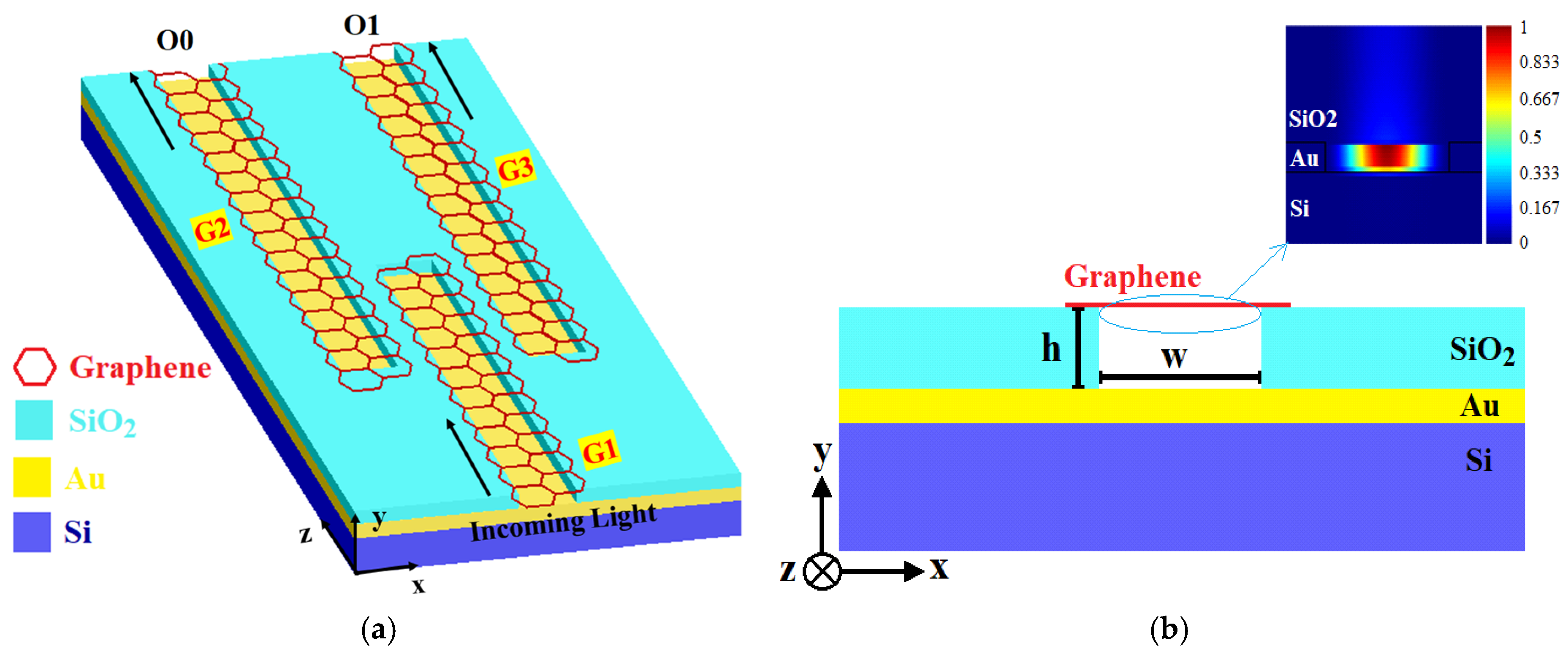
Figure 1a shows a fundamental structure for transmission and directing surface plasmon polaritons from G1 nanoribbon to G2 and G3 nanoribbons. G2 and G3 direct the surface plasmon polaritons toward O0 and O1 output ports. The bottom layer is a 200 nm silicon substrate, followed by a 40 nm gold deposition, a 100 nm silicon dioxide layer, and finally, three graphene nanoribbons. The applied voltage to these nanoribbons controls the SPP transmission via setting the Fermi level energy. It can be seen that
Figure 1a consists of three channels, including the plasmonic wells, where the SPPs excited in the G1 can penetrate into the G2 and G3, which are 10 nm apart, due to the transverse component of the electric field, and are confined near the graphene surface based on the fermi adjustment and propagate in the z-direction. A plasmonic well is considered for guiding and confining the SPPs, as shown in
Figure 1b. This figure shows a two-dimensional view of a channel (including a plasmonic well) in the xy-plane.
Surface plasmon polaritons are excited when transverse magnetic (TM)-polarized light illuminates upon the suspended graphene. As described in
Section 2, the TM illumination provides an electric field component normal to the graphene surface and a magnetic field component along the x-direction, satisfying the boundary conditions required for SPP excitation. The interaction between the incident TM field and the collective oscillations of free charge carriers in graphene induces surface current densities, governed by the graphene’s complex surface conductivity modeled using the Kubo formalism. This coupling results in the formation of bound electromagnetic surface modes, the SPPs, that propagate along the z-direction within the plasmonic well region, i.e., the air gap between the suspended graphene layer and the gold substrate. Furthermore, by applying appropriate bias voltages to the graphene ribbons, the Fermi level (or chemical potential, μ
c) is dynamically adjusted, allowing active control over the excitation and propagation of SPPs. At higher μ
c (e.g., 0.6 eV), the real part of the effective refractive index increases and losses decrease, facilitating strong SPP excitation and efficient transmission. Conversely, at lower μ
c (0.2 eV), the field confinement weakens and losses rise sharply, suppressing SPP propagation.
When transverse magnetic light illuminates the structure, it excites SPPs, which then propagate along the
z-axis in a guiding medium located beneath the graphene nanorib-bon. The magnetic field within this channel (air between graphene and gold) can be mathematically expressed.
The top air and silicon, the magnetic component is expressed as below:
where k denotes the wavenumber, and the subscripts 1, 2, and 3 correspond to the channel, the region above the channel, and the silicon layer, respectively. The coefficients A through D represent the amplitudes of the guided modes. By applying above equations, the wave equations can be reduced to the form given in Equation (3) [
22].
Within the channel, the electric fields E
y and E
z corresponding to the y and z directions are obtained from Equation (4). In this expression, ω denotes the angular frequency, ε is the permittivity, and the subscripts 0 and i (with i spanning 1 to 3) correspond to free space and the previously defined regions, respectively.
At the interface of y = 0, the boundary conditions are defined as
and
. Similarly, at the interface of y = −h, the boundary conditions are
and
. The presence of the graphene ribbon is crucial in determining these boundary conditions due to its complex conductivity, represented by σ
g. The conductivity of graphene is modeled using Kubo’s approach, which considers both the interband and intraband contributions. The component of graphene’s permittivity parallel to the surface is given by Equation (5) [
23].
Both the graphene thickness (γ) and its chemical potential (μc) are key factors determining the characteristics of the optical fields. Calculations are performed using the 3D finite-difference time-domain (FDTD) method, employing a 0.1 nm mesh size and a 5.6 attosecond simulation step to maintain accuracy. These amounts satisfy the Courant condition for achieving the convergence.
3. Results and Discussion
Manipulating the graphene nanoribbon’s chemical potential enables control over SPP transmission within the channel, which lies between the nanoribbon and a plasmonic well.
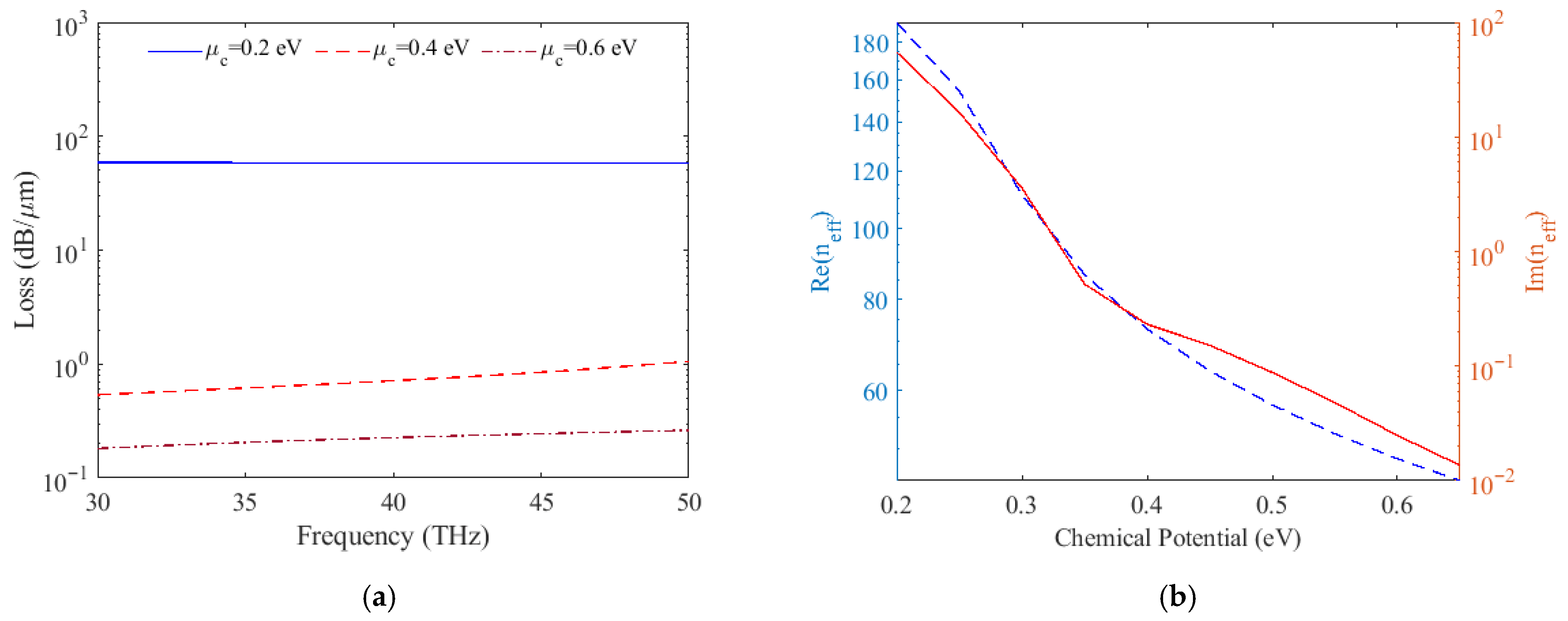
Figure 2a demonstrates how channel transmission loss changes with varying chemical potentials (0.2 eV, 0.4 eV, and 0.6 eV) across different frequencies, ranging from 58.73 to 0.28 dB/µm. A significant finding is that increasing the graphene chemical potential leads to decreased transmission loss. This effect arises from the direct impact of the chemical potential on the channel’s effective refractive index.
Figure 2b visually presents the real (Re(n
eff)) and imaginary (Im(n
eff)) parts of the effective refractive index for various chemical potentials. This figure shows that for chemical potentials between 0.2 eV and 0.6 eV at 40 THz, the real part varies from 191.73 to 45.11 and the imaginary part from 54.8 to 0.0136.
The degree of confinement in the channel is directly determined by the magnitude of the refractive index’s real part. An increased real component promotes stronger localization of surface plasmon polaritons in the channel and suppresses field spreading in the x-direction. Meanwhile, the imaginary component represents transmission loss, with higher values leading to more pronounced attenuation. This relationship is formalized by Equation (6) for transmission loss (α) [
24]:
The parameter ‘c’ refers to the speed of light in a vacuum. The chemical potential of the graphene layer can be precisely controlled by varying the electrical potential difference applied between the metal and the suspended graphene. By adjusting this bias voltage, the carrier concentration within the graphene changes, leading to modifications in its Fermi level and, consequently, its optical and electronic response. This tunability enables dynamic regulation of the device’s performance parameters, such as light absorption and modulation efficiency, making it particularly advantageous for high-speed and reconfigurable optoelectronic applications. A capacitor-based theoretical framework, presented in Equation (7), elucidates the correlation between the graphene’s chemical potential and the applied voltage (V
b) [
25].
This analysis incorporates Planck’s constant and the Fermi velocity as fundamental coefficients [
25]. As depicted in
Figure 2a, the ability of terahertz waves to transmit through the plasmonic channel is directly dependent on the graphene’s chemical potential (μ
c). When μ
c is 0.6 eV, SPP transmission is facilitated. Conversely, at μ
c = 0.2 eV, substantial losses prevent plasmon propagation beneath the graphene nanoribbons. In this study, a graphene chemical potential of 0.6 eV is selected to facilitate SPP transmission, while a reduced value of 0.2 eV is employed to effectively suppress their propagation.
According to Equation (7), graphene’s chemical potential can be precisely controlled by applying bias voltages. In particular, applying bias voltages of 1.202 V and 4.418 V results in chemical potentials of μ
c = 0.2 eV and μ
c = 0.6 eV in the graphene ribbons, respectively. For clarity, the chemical potentials associated with the three graphene nanoribbons (G1, G2, and G3 in
Figure 1a) are denoted as μ
c1, μ
c2, and μ
c3.
Figure 3 demonstrates the directional control of SPPs as they transmit through waveguide G1, where its chemical potential μ
c1 is maintained at 0.6 eV. The SPPs’ destination, either output port O0 or O1, is determined by the chemical potentials of adjacent waveguides:
(a) Activating Output O0: When μ
c2 is 0.6 eV and μ
c3 is 0.2 eV, SPPs successfully couple from G1 into waveguide G2, activating the output port O0, as illustrated in
Figure 3a.
(b) Activating Output O1: If μ
c2 is set to 0.2 eV and μ
c3 to 0.6 eV, the SPPs arriving at the end of G1 are routed into waveguide G3, subsequently reaching and illuminating output port O1. This scenario is depicted in
Figure 3b, which, along with
Figure 3a, visually details the electric field distribution of the SPP waves throughout the entire structure.
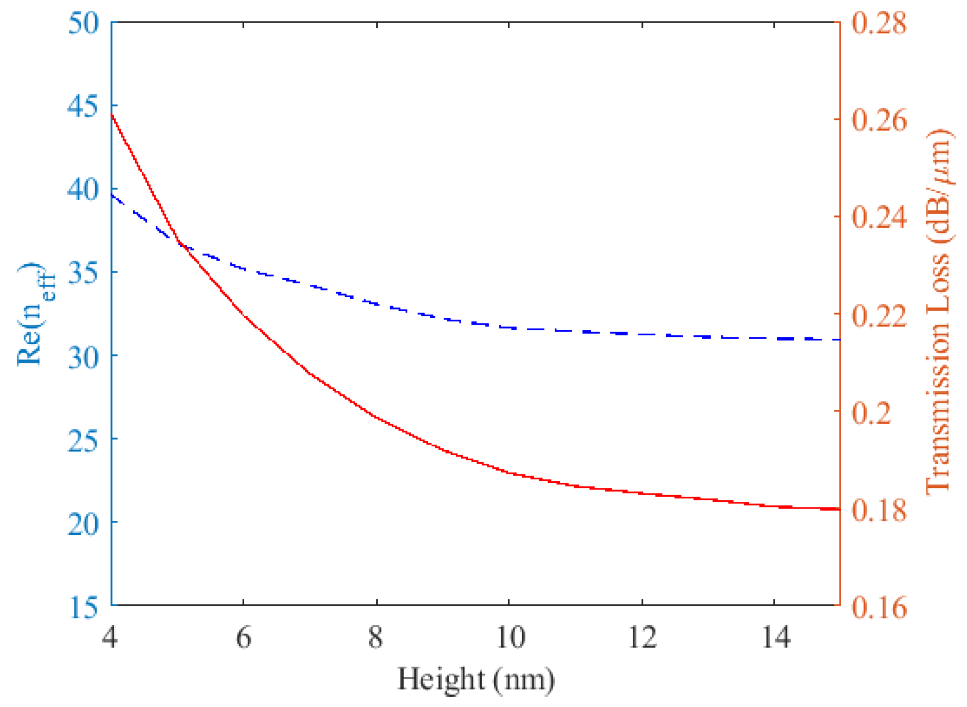
A key factor in plasmon propagation is the height of the plasmonic well, as it dictates the channel’s effective refractive index.
Figure 4 illustrates that past a 10 nm height, further increases result in only minor changes to both Re(n
eff) and propagation loss. Consequently, we selected 10 nm as the proper channel height. Since the width is in the direction perpendicular to the electric field confinement, its variation has only a minor influence on field localization unless it becomes comparable to the SPP wavelength (λ
SPP). For the designed frequency of 40 THz, λ
SPP is typically on the order of a few hundred nanometers, much larger than the 30 nm channel width. Thus, variations in width below ~30 nm have minimal impact on confinement and effective refractive index. For narrow widths (w < 50 nm), only the fundamental TM mode can exist. Thus, even substantial reductions in width will not change the number of supported modes, keeping field confinement nearly constant. Wider channels would risk supporting higher-order modes, increasing modal crosstalk and design complexity. A 30 nm wide channel ensures a subwavelength footprint, supporting ultra-dense integration in nanoscale photonic circuits (total device area 0.05 µm
2). Increasing width would enlarge the device without providing a measurable confinement advantage.
The plasmonic well was designed with a width (w) of 30 nm and a height (h) of 10 nm, based on comprehensive simulation results. These dimensions directly influence the waveguide’s performance, leading to loss of 0.188 dB/µm for μ
c = 0.6 eV and 58.32 dB/µm for μ
c = 0.2 eV. To quantify the channel’s efficiency in guiding surface plasmon polaritons, we use the figure of merit (FOM), which is the ratio of Re(n
eff) to Im(n
eff) [
26]. A higher FOM indicates superior SPP confinement and lower propagation loss. For our specific design, operating at 40 THz, Re(n
eff) is 48.36 and Im(n
eff) is 0.0248, culminating in an FOM of 1950.
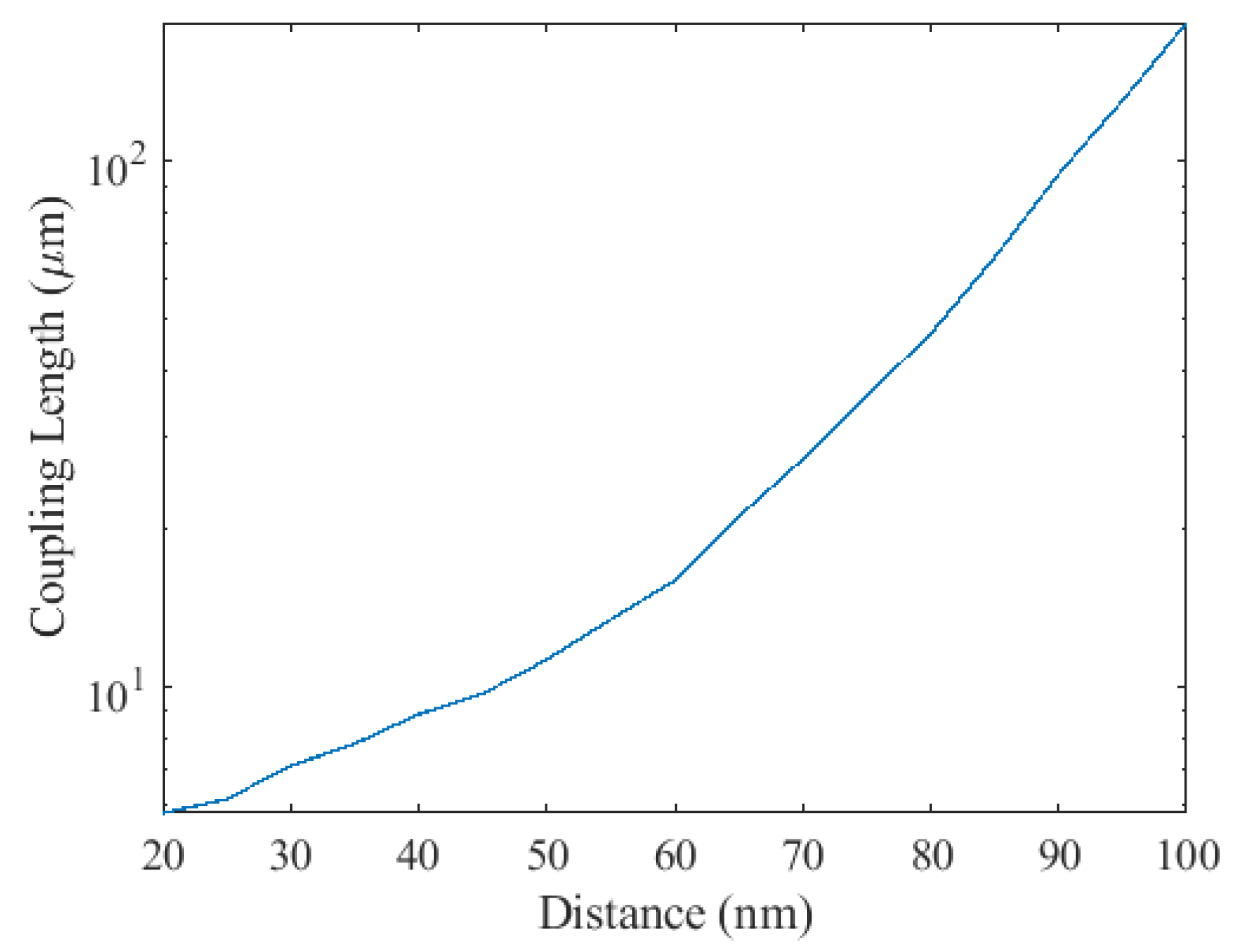
Although a high figure of merit is desirable for designing compact optical components, the inter-channel distance critically impacts the efficiency of terahertz wave coupling. Suboptimal spacing can induce detrimental coupling, leading to interference and a degradation in device functionality. To evaluate this, the coupling length, which denotes the distance over which complete optical power is transferred between neighboring channels, is calculated using Equation (8). A longer coupling length is advantageous, as it directly correlates with reduced side-field penetration and, consequently, diminished interference [
27].
The z-component of the wave vector is denoted by β, with ‘e’ and ‘o’ subscripts distinguishing even and odd modes. As presented in
Figure 5, the coupling length (L
c) exhibits an exponential increase as the distance between adjacent waveguides expands. This observed increase in L
c is partly attributable to the tight electric field confinement within the channel. While increasing channel separation is an effective strategy for minimizing interference, it is crucial to balance this with the need for a compact overall structure. Accordingly, a minimum inter-channel spacing of 40 nm has been chosen to prevent unwanted coupling.
Our simulations reveal that manipulating μ
c is an effective way to control SPP propagation. For μ
c = 0.2 eV, plasmons face significant absorption and cannot pass through the channel. Conversely, setting the chemical potential to 0.6 eV enables optical waves to propagate efficiently. This allows us to guide surface plasmon polaritons toward either output O0 or O1, depending on the specific chemical potential values applied to graphene nanoribbons G1, G2, and G3.
Figure 3 serves to validate this design as a foundational subwavelength switch for logic applications. Next, we will propose a 2-to-4 plasmonic decoder based on these principles.
4. The 2-to-4 Well-Based Plasmonic Decoder
This section details the design of a 2-to-4 subwavelength plasmonic decoder, which is an extension of the basic structure introduced in
Section 2 (
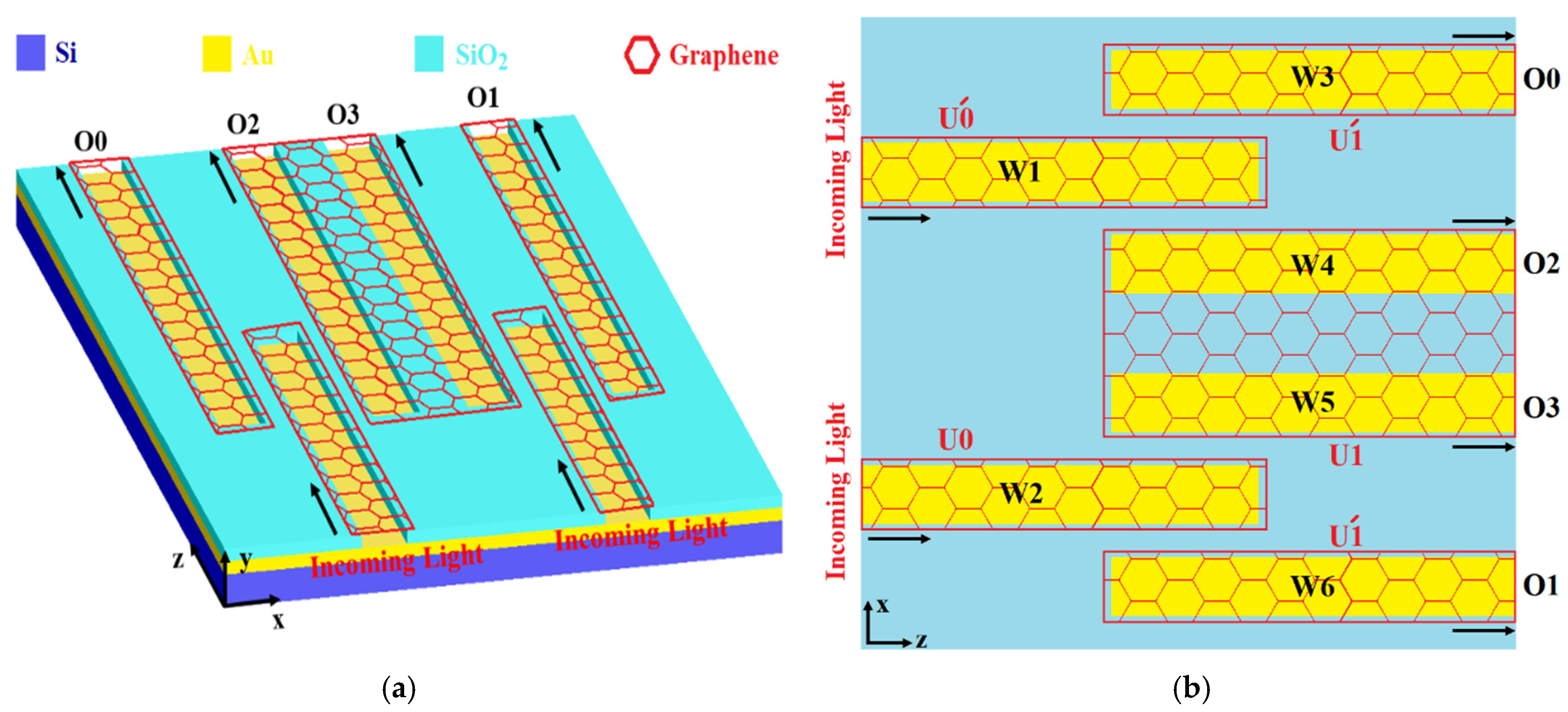
Figure 6a). The device has two inputs, U0 and U1, whose states are determined by the chemical potentials of their corresponding graphene nanoribbons. For guiding surface plasmon polaritons to the four output ports (O0 to O3), the decoder utilizes six waveguides (W1 through W6), as depicted in
Figure 6b. Control over the SPP pathways within these waveguides is achieved via five graphene nanoribbons.
Figure 6b specifically identifies the chemical potentials U0, U1, U0′, and U1′ with their associated nanoribbons. Consistent with the approach discussed in
Section 2, only two specific chemical potential values, 0.2 eV and 0.6 eV, are used to switch and direct the SPP waves. This operation adheres to a complementary rule: when U1 (or U0) is set to 0.2 eV, the corresponding U1′ (or U0′) is set to 0.6 eV, and the reverse applies as well.
The selection of a specific output port in the decoder is determined by its truth table, which interprets the electrical inputs U0 and U1.
Table 1 shows the operating conditions for this decoder. For digital signaling, a chemical potential of μ
c = 0.6 eV represents a logic 1, whereas μ
c = 0.2 eV indicates a logic 0 for the inputs.
The operation of the decoder ensures that only one output port is active at a time, depending on the input signals.
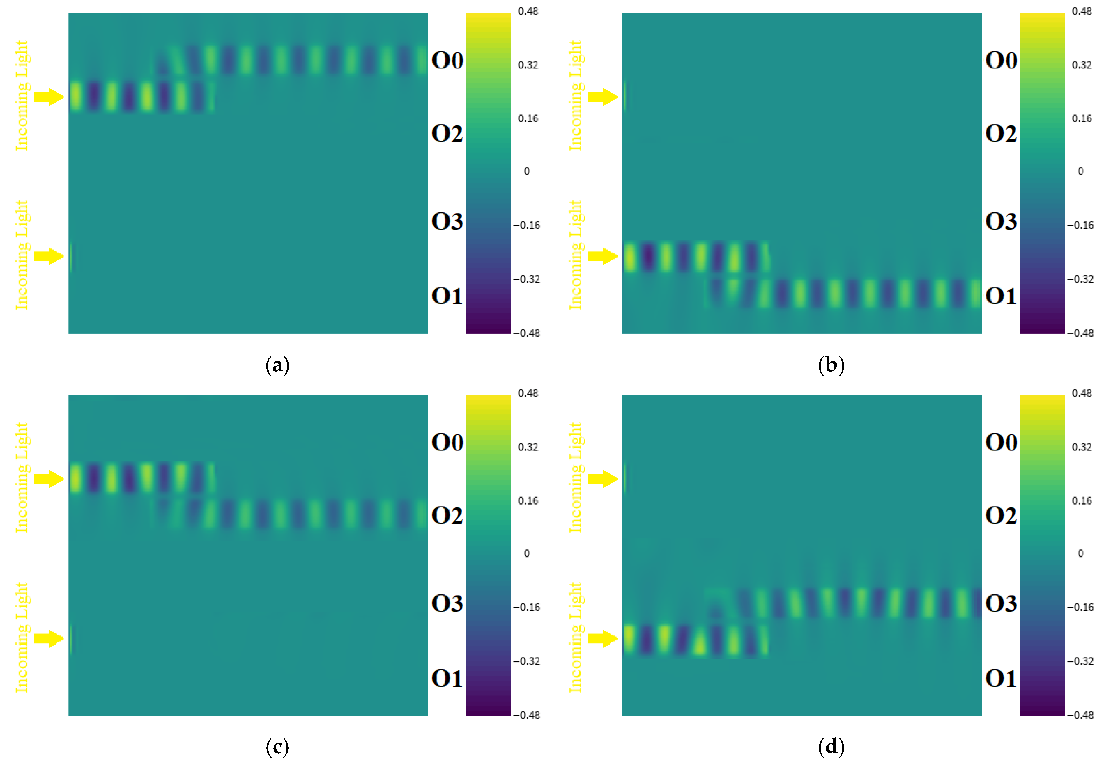
Activating O0: Setting U1 and U0 to 0.2 eV allows SPPs to move efficiently through W1 and W3, reaching output port O0, as illustrated in
Figure 7a.
Activating O1: At input potentials of U1 = 0.2 eV and U0 = 0.6 eV, optical waves follow the path from W2 to W6, activating O1 while keeping all other output ports inactive (
Figure 7b).
Activating O2: Output port O2 becomes active when SPPs are transmitted through waveguides W1 and W4. This occurs under the condition U1 = 0.6 eV and U0 = 0.2 eV, as shown in
Figure 7c.
Activating O3: At U1 = U0 = 0.6 eV, SPPs successfully propagate through W2 and W5 to reach O3, utilizing the low-loss propagation depicted in
Figure 2a. This configuration activates O3, while all other outputs remain off (
Figure 7d).
Table 2 provides a comprehensive look at the decoder’s performance by detailing the optical power at O0 to O3 ports across four distinct operational cases. In case 1, the normalized powers for outputs O0, O1, O2, and O3 are 98.7%, 0.01%, 0.02%, and 0.01%, respectively. Case 2 shows the normalized powers of 0.01%, 98.6%, 0.01%, and 0.02% for the same output ports. For case 3, the observed normalized power values are 0.02% at O0, 0.01% at O1, 98.7% at O2, and 0.02% at O3. Finally, case 4 demonstrates power outputs of 0.01% for O0, 0.02% for O1, 0.02% for O2, and 98.7% for O3.
Due to the extremely compact footprint of the designed structure (approximately 0.05 µm
2), the simulated transmission spectra for the different working conditions exhibit very similar behaviors. As indicated in
Table 2, the transmission efficiency for each activated output port remains consistently high, in the range of 98.6–98.7%, confirming the efficient routing capability of the plasmonic decoder. Moreover, as shown in
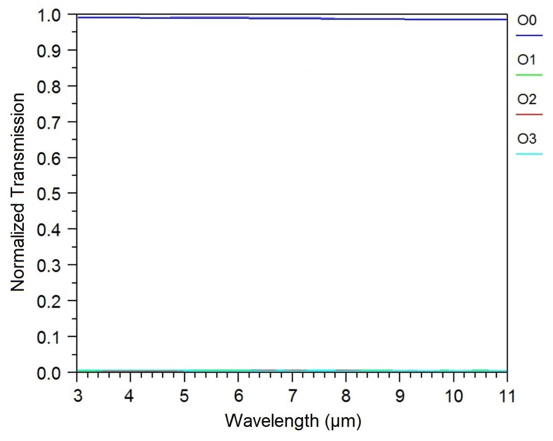
Figure 2a, the propagation loss is minimal when the graphene chemical potential is set to µ
c = 0.6 eV, corresponding to the low-loss state of the device. To further clarify this point and strengthen the discussion, the simulated transmission results associated with
Figure 7a have shown in
Figure 8. These additions provide a more comprehensive understanding of the transmission performance and confirm the robustness of the proposed design across all operational conditions.
The logic 0 margin (M
0) and logic 1 margin (M
1) are critical parameters used to assess the designed structure’s performance under the worst cases. M
0 quantifies the highest value considered as logic 0, while M
1 defines the lowest value recognized as logic 1. Based on the data in
Table 2, M
0 for our structure is 0.02%, and M
1 is 98.6% (demonstrated in Case 2). To further illustrate the decoder’s capability to clearly distinguish between logic 0 and logic 1, we employ the contrast ratio (CR), as detailed in Equation (9). A greater CR value directly makes more difference between the logic 0 and 1 signals at outputs [
28].
The proposed plasmonic device exhibits a contrast ratio of 36.93 dB, calculated based on an M
0 value of 0.02% and an M
1 value of 98.6%. Furthermore, crosstalk (CT), representing the undesirable coupling of surface plasmon polaritons between adjacent waveguides, is a significant factor in assessing overall decoder performance. Equation (10) defines crosstalk, with P
0 and P
1 representing the optical powers at the outputs for logic levels 0 and 1, respectively [
29].
As presented in
Table 2, the crosstalk values for output ports O0 to O3 are determined to be −36.93 dB, −36.92 dB, −36.93 dB, and −36.93 dB, respectively. Consequently, the highest observed crosstalk in the structure is −36.93 dB. To effectively assess the performance of the designed decoder, it is useful to conduct a comparative analysis against other existing devices. Accordingly,
Table 3 summarizes the obtained results covering the device’s area, contrast ratio, crosstalk, and loss, along with corresponding data reported in previous literature.
The size of optical devices is a critical consideration in the design of integrated circuits. Conventional Mach-Zehnder interferometer structures are typically large on the order of several micrometers and often suffer from inefficient interference, making them unsuitable for compact optical systems [
33,
34,
35,
36]. Similarly, photonic crystal-based devices tend to be too bulky for high-density integration. Although resonant cavity-based designs can achieve some degree of miniaturization [
37,
38,
39,
40], fabricating them at sub-micrometer scales remains a significant challenge. Nevertheless, the inherent scalability of photonic crystal architectures continues to hold promise for future developments. In contrast, plasmonic structures provide a major advantage: they can process and decode optical signals at both micro and nanoscale dimensions. The proposed decoder exemplifies this capability, occupying only 0.05 µm
2, which is substantially more compact than previously reported designs [
18,
19,
20,
30,
31,
32]. This compactness represents one of its principal advantages. Performance-wise, the decoder also demonstrates excellent optical characteristics. Its contrast ratio of 36.93 dB indicates a strong ability to distinguish clearly between logic states 0 and 1. This CR is similar to those reported in earlier works [
19,
20,
30,
31,
32], primarily due to the enhanced confinement of SPPs within the plasmonic well. Such tight confinement not only improves signal distinction but also results in low crosstalk, calculated at −36.93 dB.
The incorporation of suspended graphene significantly improves carrier mobility, which in turn enhances the optical confinement within the waveguide channel. This stronger confinement ensures that the electromagnetic field is more tightly bound to the propagation region, reducing energy leakage into the surrounding material. As a result, the lateral electric field experiences minimal dispersion, contributing to a remarkably low propagation loss of only 0.188 dB/µm. Such low loss is particularly advantageous for maintaining signal integrity over longer distances within compact photonic circuits. Considering the ultra-small footprint of the device, this level of loss not only supports efficient signal transmission but also allows for high-density integration of multiple optical components on a single chip. Consequently, the combination of suspended graphene and optimized channel design provides a practical and effective approach for developing low-loss, high-performance optical circuits suitable for advanced photonic applications. Overall, the proposed 2-to-4 plasmonic decoder achieves notable improvements in both compactness and transmission loss, highlighting its potential for use in advanced optical circuit technologies.
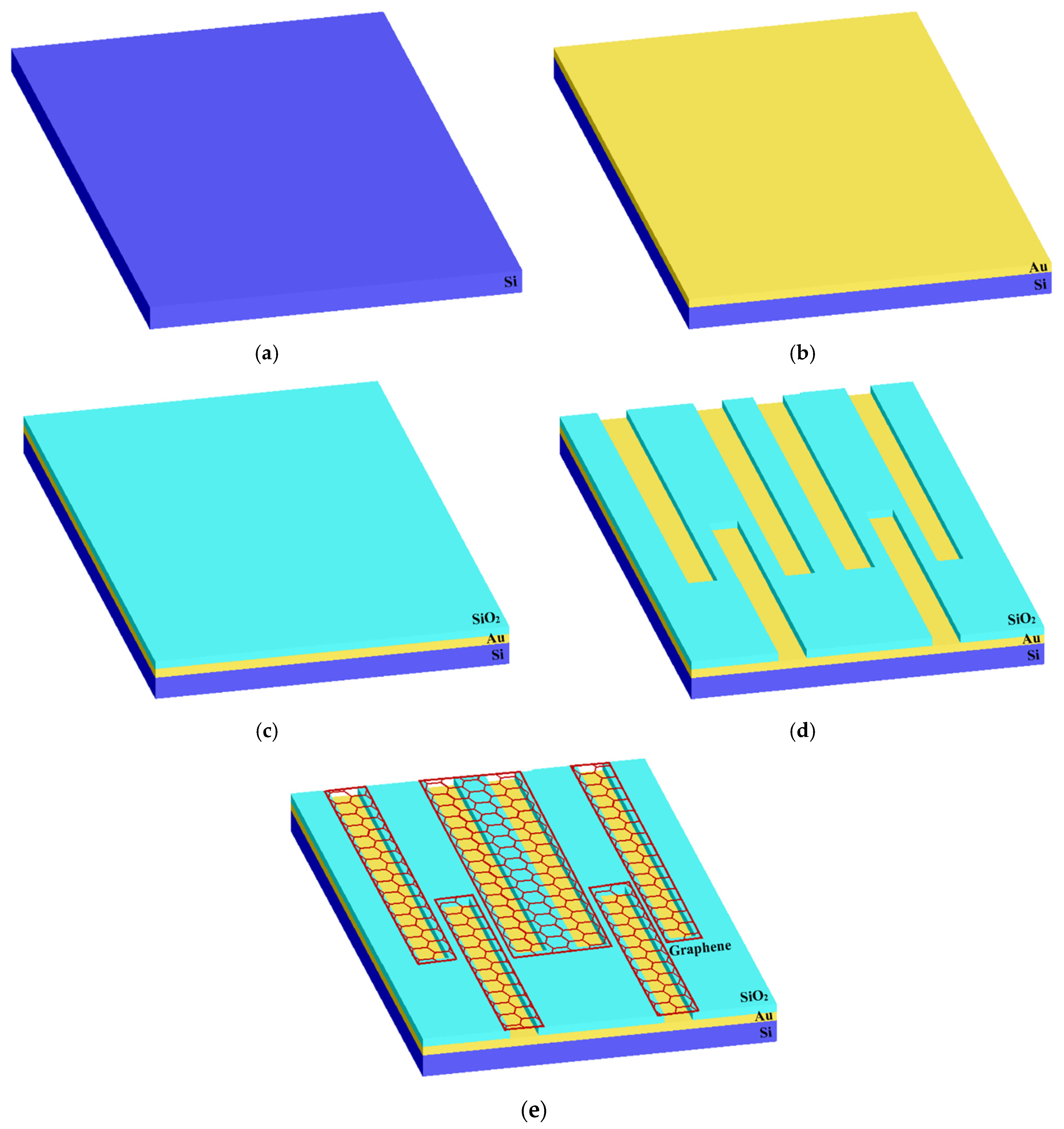
As illustrated in
Figure 9, the proposed structure is created through a five-step fabrication process. It begins with a silicon substrate, followed by the deposition of a thin gold film and then a silicon dioxide layer. Grooves are precisely formed using electron beam lithography and reactive ion etching techniques [
41,
42]. The process concludes with the transfer of graphene ribbons [
43].
The designed 2-to-4 plasmonic decoder performs a fundamental digital logic function in the optical domain using surface plasmon polaritons. This capability is central to developing optical logic circuits, including optical multiplexers/demultiplexers, arithmetic logic units, memory addressing systems, and programmable photonic logic arrays. Because the device demonstrates high contrast ratio and low crosstalk, it can distinguish logic states with high fidelity, a critical requirement for cascaded logic operations in computing architectures.
