Abstract
This study presents the Raman spectral characteristics and selected electrical parameter measurements of WS2 films deposited by magnetron sputtering on sapphire and subsequently sulfurized. The analysis of the Raman spectra focuses on the positions and shifts of the E12g and A1g vibrational modes. The effects of different sputtering times on WS2 films and the corresponding activation energy values were also investigated. From both physical and experimental perspectives, the Raman spectral features of WS2 films were found to depend on the laser excitation wavelengths (532 nm and 632.8 nm) as well as on possible crystallographic defects and variations in the excitation point position. These defects have a significant influence on both the Raman spectra and the activation energies of the studied samples. The calculated activation energies (~ 0.15–0.19 eV) of the conduction charge carriers correlate with shallow defect-related energy levels indicated by the Raman characteristics.
1. Introduction
The main goal of this study is to analyze the Raman spectra and obtain information about the morphology of the WS2 material versus position of Raman bands. Another goal was to obtain the activation energies of the charge carriers by electrical measurements and calculations, estimate their origin and correlate it with the Raman spectroscopy results. We investigate nanostructured tungsten disulfide (WS2) films on sapphire substrates as a material for electronic applications, specifically as a gas sensor. For this, we need semiconductor material with a high surface-to-volume ratio. WS2 has the largest direct band gap of about approximately 2.1 eV and indirect band gap of 1.3 eV. Its most distinguished characteristics are the transition from indirect band gap to direct band gap, when thinned down from a bulk to a monolayer.
The most prominent Raman bands of WS2 are the E12g and A1g modes which are associated with in-plane and out-of-plane vibrations of W and S atoms. These two main vibrations are characteristic of layered transition metal dichalcogenides with a hexagonal structure. The E12g band corresponds to the in-plane vibrations of sulfur and tungsten atoms in the layer, where the metal and chalcogen atoms vibrate in opposite directions. The frequency of the E12g vibrations varies depending on the number of layers of the material. In the WS2 monolayer, the E12g mode is located at approximately 356 cm−1. The A1g mode represents oscillations of sulfur atoms that move perpendicular to the plane and out of plane, whereas the tungsten atoms remain relatively motionless at the equilibrium position (see Figure 1) [1,2,3,4,5]. Position of the A1g band peak is also sensitive to the number of layers of WS2; for example, in a monolayer, it is located at approximately 418 cm−1, while in thicker layers, it shifts to higher wavenumber values. This shift is due to interactions between the layers of the material. The difference between both peaks serves as a sensitive indicator of the number of layers and interlayer interactions of WS2. It has been found experimentally [6] that when WS2 is a monolayer material, the difference between the dominant bands is less than ~60 cm−1. In addition to the bands with E12g and A1g peaks, the Raman spectrum of WS2 also contains higher-order vibrational modes, namely 2LA(M) and 2LA(T) [7]. Similar Raman features are also found in other layered transition metal dichalcogenides, such as WSe2 and MoS2. The main difference in the Raman spectra of WS2, WSe2 and MoS2 is the number and position of their characteristic peaks. MoS2 typically exhibits two prominent peaks, the in-plane E12g mode around 383 cm−1 and the out-of-plane A1g mode around 407 cm−1. In contrast, WSe2 exhibits more peaks in its first-order spectrum, peaks located around 137 and 248 cm−1 and mode A1g around 251 cm−1. The position of the single peak in few-layer samples of WSe2 shifts with the number of layers, unlike MoS2, which exhibits a clear evolution in the spacing between its two main modes [3,8,9,10].
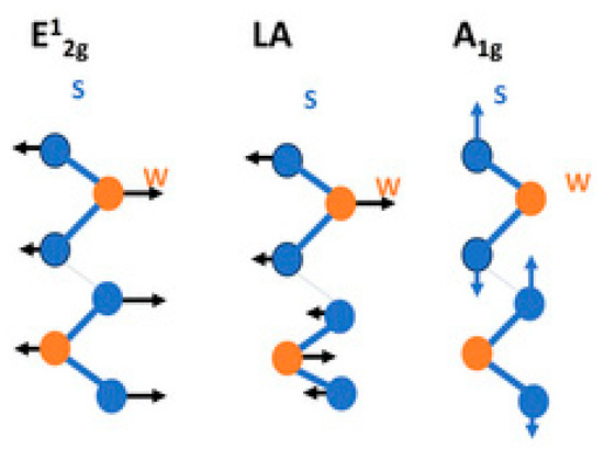
Figure 1.
Schematic diagram of the first-order Raman active modes of WS2. Illustration of atomic displacements for the in-plane phonon mode E12g, out-of-plane phonon mode A1g, and 2LA vibrational mode in WS2. Reprinted from Ref. [2].
Analysis of the characteristic Raman modes (E12g and A1g) provides insights into the crystalline quality, structural defects, and internal strain, all of which significantly influence the electrical and chemical behavior of the material. Shifts or intensity variations in the Raman bands upon gas exposure allow the monitoring of interactions between WS2 and gas molecules, thereby contributing to the understanding of the charge transfer mechanisms involved in gas sensing. Furthermore, Raman spectroscopy enables the identification of different structural phases (e.g., 2H and 1T), which exhibit distinct electrical conductivities and consequently different sensing responses. Due to its capability for in situ measurements, Raman spectroscopy is also well suited for studying the dynamics of gas adsorption and desorption processes, making it an indispensable tool for optimizing the sensitivity, stability, and repeatability of WS2-based gas sensors [11,12,13].
2. Materials and Methods
2.1. Preparation of WS2 Films
The preparation of WS2 films consists of the following steps. The substrate material is sapphire, and the plane on which the films were deposited has a crystallographic orientation C-plane [0001] (Cryscore optoelectronics Ltd., Jiaozuo, China). Here, we expect van der Waals epitaxy to play a major role as C-plane provide a hexagonal structure, which may align with WS2 films under certain conditions. All sapphire substrates were cleaned ultrasonically using a sequence of acetone, isopropylalcohol, and deionized water.
WS2 films were deposited onto polished C-plane sapphire substrates by magnetron sputtering from a WS2 target that was declared by the manufacturer as stoichiometric (99.9% purity, fy MaTeck, Juelich, Germany) at room temperature. The sputtering vacuum chamber was evacuated to a pressure below 10–4 Pa before starting deposition using a turbo pump (Turbo HiPace 2300, fy Pfeiffer Vacuum, Prague, Czech Republic). Argon (99.999% purity, fy Linde Gas, Bratislava, Slovakia) inert gas flow 27 sccm was controlled by a mass flow controller (fy MKS Inc., Brno, Czech Republic). The total argon sputtering gas pressure was kept at 0.5 Pa and adjusted by a piezoceramic valve. A sputtering power of 45 W was used. The distance between the substrate and the WS2 target was approximately 75 mm, and the substrate holder was in a constant position during sputtering without rotation. The thickness of WS2 films was measured after deposition by Talystep through a photolithographically prepared step.
The second technological step was sulfurization. WS2 films of different thickness were placed in the center of the heating zone together with another zone of sulfur powder (1 g of sulfur) and heated at a rate of 25 °C/min to a temperature of 800 °C. The annealing time at 800 °C was 30 min. Sulfurization was carried out in a nitrogen atmosphere at ambient pressure. After sulfurization, the temperature was decreased at a rate of 20 °C/min. Spontaneous cooling followed from a temperature of 200 °C.
The basic technology characteristics of the three samples presented in this work are in Table 1. The atomic ratio of W:S and impurities in the deposited WS2 nanostructures were not investigated.

Table 1.
Basic technology characteristics of the three samples of WS2.
2.2. Characterization of WS2 Films
Raman measurements of the WS2 material sputtered on sapphire and subsequently sulfurized were conducted using two Raman spectrometers. The first Raman investigations were performed on confocal Raman microscope (alpha 300R, WITec, Ulm, Germany) using an excitation laser with a 532 nm wavelength. The laser power was kept below 1 mW. The spectral resolution of the entire Raman system was about 0.75 cm−1. The second Raman investigations were carried out through micro-Raman measurements of the deposited WS2 films performed using an ISA Dilor-Jobin YvonSpex Labram (HORIBA group division (FRANCE)) confocal system with 632.8 nm radiation from a He-Ne laser, using a back-scattering geometry and a laser power of 5 mW. Microscope objectives 10× and 80× were used to focus the laser beam onto a spot of approximately 5 µm in diameter, and to collect the scattered light which then passed through the spectrometer onto a CCD detector. Furthermore, a confocal hole with a diameter of 600 µm, a spectrograph entrance slit of 600 µm, and 600 grooves/mm diffraction grating were employed. Calibration measurements performed on single crystalline Si (100) showed a measurement uncertainty of ±2 cm−1 in comparison with the catalogue value for silicon 520.7 cm−1. All Raman spectra were obtained at room temperature. At least three measurements of Raman spectra were performed on individual samples at different locations. After Raman investigations, the morphologies of WS2 films were observed by field emission scanning electron microscopy (FESEM, Quanta FEG 250, FEI Company, Hillsboro, OR, USA) in secondary electron (SE) mode. Electrical characterization was performed using the Ossila Four Point Probe (Ossila Ltd., Sheffield, UK), and activation energy calculations were carried out based on the Arrhenius plots of the samples.
3. Results and Discussion
3.1. FESEM Observations
The nanostructured WS2 films were formed by sputtering WS2 stoichiometric bodies of 14 nm, 30 nm and 45 nm thickness and by sulfurization under the same conditions for all samples listed in Table 1. Figure 2, Figure 3 and Figure 4 show the morphologies of nanostructured WS2 films using FESEM. In Figure 2, a discontinuous seed layer of crystals is seen. We estimate that WS2 of thickness 14 nm contains 20 layers [14]. In Figure 3, growing crystals are clearly visible, and in Figure 4, a flake nanostructure of WS2 is developed. The WS2 flakes are not uniformly distributed and are differently oriented. WS2 crystals have strong in-plane chemical bonds but weak interplanar bonds, so they can form nanoflakes or nanolayers that are nanometers thick in one direction but can be micrometers wide and their active surface area can exceed 1000 square meters per gram [1,15].
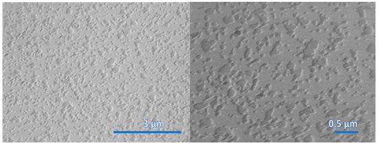
Figure 2.
SEM images of surface morphology of WS2 film (sample WS92A) grown on sapphire substrate. The thickness of the deposited WS2 film is 14 nm.
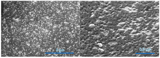
Figure 3.
SEM images of surface morphology of WS2 film (sample WS92B) grown on sapphire substrate. The thickness of the deposited WS2 film is 30 nm.
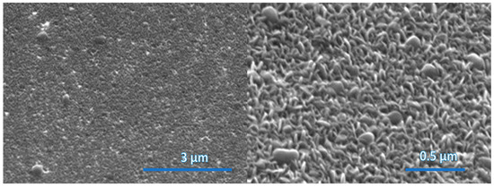
Figure 4.
SEM images of surface morphology of WS2 film (sample WS91A) grown on sapphire substrate. The thickness of the deposited WS2 film is 45 nm.
3.2. Raman Spectroscopy
Figure 5, Figure 6 and Figure 7 show the Raman spectra of nanostructured WS2 films. For an excitation wavelength of 532 nm, we observed prominent Raman peaks of WS2 at 350 cm−1 and 417–418 cm−1. The first mode is asymmetric, and after deconvolution, it is clear that it is composed of the 2LA peak at ~350 cm−1 and the E12g at 355 cm−1. The overlap of the E12g and 2LA bands makes their location less reliable. Wavenumber separation of A1g and E12g Raman phonon modes excited by green laser is approximately 67 cm−1 for sample WS92A, 67 cm−1 for sample WS92B, and 69 cm−1 for sample WS91A.
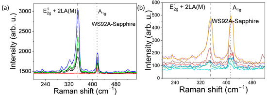
Figure 5.
Raman spectra of WS92A (200–540 cm−1) from multiple surface spots of a 14 nm WS2 film: (a) five spots under 532 nm excitation; (b) seven spots under 632.8 nm He–Ne excitation.
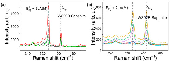
Figure 6.
Raman spectra of WS92B (200–540 cm−1) from a 30 nm WS2 film: (a) four surface spots under 532 nm excitation; (b) ten surface spots under 632.8 nm He–Ne excitation.
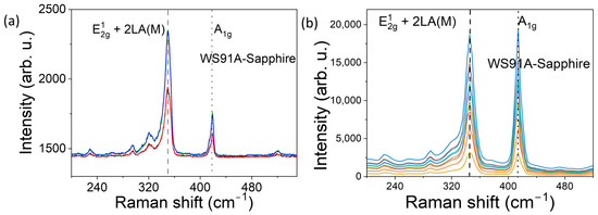
Figure 7.
Raman spectra of WS91A (200–540 cm−1) from a 45 nm WS2 film: (a) four surface spots under 532 nm excitation; (b) ten surface spots under 632.8 nm He–Ne excitation.
In the graphically recorded Raman characteristics of WS2 samples obtained by excitation with a He-Ne laser (632.8 nm), two bands with centers at 345 cm−1 to 349 cm−1 are dominant, which approximately corresponds to the E12g mode (in-plane vibrations of W and S atoms) and a band with a center at approximately 413–415 cm−1, which corresponds to the A1g mode (out-of-plane vibrations of S atoms). The Raman characteristics of WS2 of the 632.8 nm laser excitation (Figure 5b, Figure 6b and Figure 7b) confirmed the fact that the distance between the dominant bands A1g and E12g increases with the increase in the thickness of the WS2 film, i.e., with the increase in the number of layers. The difference between the recorded peaks of the dominant bands of the three samples under study is approximately 66 cm−1, 67 cm−1 and 68 cm−1. As the thickness of WS2 films increases from WS92A and WS92B to WS91A, the intensity of the Raman response also increases. The intensity ratio A1g/E12g of the Raman peaks varies depending on samples. The ratio is greater than 1 and increases with thickness samples. With the increase in the number of WS2 layers, the band with the E12g peak shifts to lower wavenumbers (see Table 2).
Table 2.
The value of separation and intensity ratio of the A1g and E12g.
3.3. Analysis of Raman Spectral Characteristics of WS2 Films
In the Raman spectra of some locations of the WS92A and WS92B samples, one of the main E12g bands is missing when excited by both lasers, so we do not see in-plane vibrations of tungsten and sulfur atoms. The decrease in the intensity of the E12g mode may be related to defects, mainly sulfur vacancies, or amorphous regions in the WS2 layers, where certain vibrations are not effectively scattered and the mode may be invisible and lost in the noise. This effect, of E12g vibrations not being effectively scattered, was observed most in the thinnest WS92A film when excited by both lasers. In multilayer WS2, the layers are bound to each other by van der Waals forces, and these interlayer interactions can change the dynamics of vibrations, which also leads to the attenuation of the E12g mode. According to [3,4,14], E12g vibrations can be suppressed even in monolayers. We assume that lattice defects have a significant effect on the Raman spectrum of the studied samples. The shift of the E12g band to the side of smaller wave numbers and the moving away of the E12g and A1g bands from each other can be attributed to the effect of defects, and we mainly consider the effect of vacancies due to the deficit of sulfur atoms in the technological process. Vacancies change the local strain in the lattice. Defects disrupt the periodicity of the crystal lattice, which leads to a decrease in phonon coherence and therefore to a broadening (FWHM) of the full width at half maximum of both characteristic bands of E12g and A1g. The FWHM of both dominant modes of an ideal WS2 crystal or monolayer is 3 to 6 cm−1. The broadening of bands A1g and for E12g of samples WS92A, WS92B and WS91A when excited by a 532 nm laser and 632.8 nm laser shows a decreasing trend (see Table 2).
In addition to the effect of the shift of the dominant band E12g relative to A1g, we also observed other modes that are not typical in the Raman spectrum of WS2 but may also be related to defects in the lattice, different orientations of layers or domains in the material, namely modes in the low-frequency region of the Raman spectrum at 260 cm−1, 290 cm−1 and 320 cm−1 depending on the excitation.
The effect of higher photon energy of the excitation laser and shorter wavelength (532 nm) was manifested by the enhancement of the E12g mode compared to the A1g mode in all WS91A, WS92A and WS92B samples (see Figure 5a, Figure 6a and Figure 7a). The ratio of the peak intensity of the A1g to E12g bands ranges from 0.5 to 0.7 depending on the thickness of the WS2 film in the Raman spectra excited by the 532 nm laser. At the same time, the intensity of the E12g Raman modes excited by the green laser at most of the monitored locations of the WS92A and WS92B samples is higher in these thinner WS2 layers compared to the Raman response of the thickest WS91A sample (see Figure 7a vs. Figure 5a and Figure 6a).
We explain the decrease in Raman intensity at a WS2 film thickness of 45 nm (WS91A) for green excitation by the fact that the intensity of Raman modes may decrease with increasing WS2 thickness if there are more homogeneities that reduce the effective Raman response.
The effect of the lower photon energy of the He-Ne laser and its longer wavelength (632.8 nm) was manifested by the enhancement of the A1g mode with a stronger Raman signal compared to the excitation of the A1g mode by a green laser, which is related to better penetration into the material of the WS2 samples. For excitation with a 632.8 nm laser, the ratio of the intensity peaks of the A1g to E12g bands is ~1 and does not depend on the thickness of the WS2 film of the monitored samples. The absence or weakening of the E12g mode in the Raman spectrum of WS2 can also be the result of the influence of experimental factors, such as the back-scattering configuration of the experiment, but also problems related to the observed sample, like impurities or inhomogeneities of the layer surface; the choice of the monitored location on the sample can also affect the intensity of the Raman signal.
We did not analyze the 2LA mode in the samples studied. The second-order longitudinal acoustic mode 2LA in the Raman spectrum of WS2 excited by a He-Ne laser may be present or overlapped or absent or significantly attenuated near the E12g band. To ensure the detection of the 2LA mode, it is important to optimize the experimental conditions or to make a theoretical estimate of its position by calculation.
Since we could not perform a compositional analysis of the studied WS2 films, it is apparent from the study of available sources that there are interrelationships between chemical composition and structure. It was found that chemical composition of WS2 films (determined, e.g., by EDS) has a direct influence on their Raman spectral characteristics. Deviations from the ideal W:S ratio of 1:2 typically indicate sulfur deficiency and the formation of sulfur vacancies, which strongly affect the vibrational modes of the material. Raman spectra of sulfur-deficient WS2 commonly exhibit a slight blue shift of the in-plane E12g mode and a red shift with reduced intensity of the out-of-plane A1g mode. These spectral changes originate from local distortions of W–S bonds and modifications in interlayer coupling caused by missing sulfur atoms. Additionally, the presence of sulfur vacancies often leads to band broadening or the emergence of defect-induced Raman features, reflecting increased structural disorder. The combined analysis of EDS and Raman data thus provides complementary insight: while EDS confirms the elemental composition, Raman spectroscopy reveals the structural and bonding consequences of sulfur deficiency. Importantly, a moderate concentration of sulfur vacancies can enhance the gas sensing performance of WS2 by providing additional active sites for gas adsorption and charge transfer, highlighting the crucial interplay between composition, structure, and functionality [13,16,17].
3.4. Electrical Characterization of WS2 Films
The measurement setup consists of four non-destructive, round, soft-tipped probe contact used to measure sheet resistance. The system operates by applying a DC current between the two outer probes and measuring the resulting voltage drop between the two inner probes. All four probes are equally spaced, with a distance of 1.27 mm between each probe. For the most accurate results, measurements are typically taken at the center of the sample. From the Arrhenius equation, we know that
where T is temperature, K is the Boltzmann’s constant, Ea is activation energy, σ is conductance (S) dependent on temperature, and σ0 is constant.
Sample WS92A, deposited at 1 min, was not characterizable by the four probe method, due to very high resistivity. Thinner films have comparatively higher resistivity, which is beyond the compliance of the instrument. The WS2 films deposited in 2 min (WS92B) and 3 min (WS91A) and sulfurized with 1 g of sulfur have extremely high sheet resistance of 260 MΩ and 58 MΩ, respectively. Since sheet resistance is an intrinsic property of the material, it reflects the electrical characteristics of the sample. The measurements were taken at ambient room conditions. To avoid for potential variations in sheet resistance due to heat loss, each reading was recorded after achieving thermal equilibrium. The measurement temperature range is between 21 °C and 112 °C.
All resistance values given are the average of the measured values, as each measurement is made after reaching thermal equilibrium, so slight inaccuracies or errors may occur. Mathematically, the graph was linearly approximated with R2 = 0.99 with negligible inaccuracies. Slope (92B—blue) = −0.96512 ± 0.00987, and slope (91A—orange) = −0.75897 ± 0.00753.
From the Arrhenius plots (see Figure 8 and Table 3 and Table 4), the activation energy for the conductivity of sulfurized WS2 films was determined to be Ea ~ 0.19 eV for the layer sputtered for 2 min (WS92B) and Ea ~ 0.15 eV for the layer sputtered for 3 min (WS91A). These (low) activation energy values indicate that the electrical conductivity in the investigated temperature range is conditioned by charge carriers at shallow energy levels in the energy gap, i.e., defects (e.g., grain boundaries) and surface disorder states and traps (e.g., sulfur vacancies). The conductivity, as evident from the plot on Figure 8, therefore increases with temperature due to thermal excitation of charge carriers from these shallow states into the conduction band. Intrinsic conductivity, which is controlled by an intrinsic band mechanism, cannot be considered. In the case of sputtered WS2 layers, the activation energy would have to be approximately Eg/2 ≈ 1.0 eV (Eg ≈ 2.3 eV) to excite electrons from near the Fermi level. From the perspective of research and development of WS2 materials, this means that WS2 in a state of low intrinsic conductivity shows increased sensitivity to surface changes, because energy defect states close to the conduction band (with a depth of ~0.15–0.19 eV) are easily ionized. For even small energy stimuli, e.g., temperature or change in surface potential or adsorption of molecules, if a gas molecule binds to the surface, the local carrier density changes and the conductivity of WS2 changes noticeably even at low analytic concentrations. The low activation energy in WS2 material means that the conductivity is controlled by shallow defect states, which is advantageous for sensor applications in gaseous environments. Both DFT (density functional theory) calculations and DLTS (deep level transient spectroscopy) measurements on layered (monolayer and multilayer) WS2 show that sulfur vacancies form localized defect states just below the conduction band, i.e., they behave as shallow donor levels. This is also the reason why WS2 films mostly exhibit n-type conductivity [18,19].
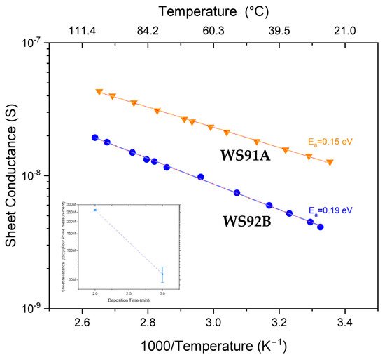
Figure 8.
Arrhenius plot of two samples of WS2 (WS91A and WS92B). Inset: x-axis is linear scale of deposition time in minutes, y-axis is at logarithmic scale of sheet resistance in Ω/□.
Table 3.
Calculated activation energy values.
Table 4.
The separation of the A1g and E12g vs. activation energies.
4. Conclusions
From a microscopic point of view, all tested samples have a relief character; therefore, it is not possible to record Raman maps of the samples. However, at individual points of all samples, it is possible to identify the crystalline morphological structure of WS2 using the characteristic bands E12g and A1g when excited by the 532 nm laser and the 632.8 nm laser. According to the high photoluminescence background of the spectra, it can be concluded that the WS2 nanoflakes layer contains crystallographic defects of various types. The intensity of the E12g mode band is also probably slightly reduced in connection with layer defects. Defects also suppress or scatter out-of-plane vibrations, so the high intensity of the A1g mode decreases relative to E12g. The presence of defects in the lattice and different orientations of layers or domains are also indicated by sidebands next to the dominant bands, especially in the low-frequency part of the spectra. The asymmetric shape of the E12g band also indicates lattice defects and defect zones in the film. The shift of the E12g band to the side of smaller wavenumbers after excitation by a He-Ne laser and the moving away of the band peaks from each other with increasing material thickness can be interpreted as the influence of the increasing number of defects, for example grain boundaries, interstitial impurities, amorphous regions, but mainly sulfur vacancies, which change the local strain in the lattice; subsequently local defects also affect the energy structure of WS2, and specifically sulfur vacancies lead to donor states near the conduction band.
From the Arrhenius plots, the activation energy for the conductivity of sulfurized WS2 films was determined to be Ea ~ 0.19 eV for the film sputtered for 2 min (WS92B) and Ea ~ 0.15 eV for the film sputtered for 3 min (WS91A). The low activation energy indicates that the conductivity of the WS2 material produced in our laboratory is controlled by the detected shallow defect states, which is advantageous for sensor applications in gaseous environments.
Author Contributions
Conceptualization, M.K. and I.H.; methodology, M.K., M.S. and. I.H.; validation, M.S., I.H. and. D.G.; investigation, N.K., I.K. and V.Ř.; writing—original draft preparation, M.K.; writing—review and editing, N.K. and I.H.; visualization, I.K.; funding acquisition, I.H. All authors have read and agreed to the published version of the manuscript.
Funding
The work was supported by the Scientific Grants Agency of the Ministry of Education, Research, Development and Youth of the Slovak Republic and of the Slovak Academy of Sciences No. 1/0480/25 and No. 1/0435/25, and by the Slovak Research and Development Agency under contract No. APVV-21-0278.
Data Availability Statement
The original contributions presented in this study are included in the article. Further inquiries can be directed to the corresponding author.
Conflicts of Interest
The authors declare no conflicts of interest.
References
- Berkdemir, A.; Gutierrez, H.R.; Botello-Méndez, A.R.; López, N.P.; Elías, A.L.; Chia, C.; Wang, B.; Crespi, V.H.; Urías, F.L.; Charlier, J.C.; et al. Identification of individual and few layers of WS2 using Raman Spectroscopy. Sci. Rep. 2013, 3, 1755. [Google Scholar] [CrossRef]
- Okeke, C.; Juma, I.; Cobarrubia, A.; Schottle, N.; Maddah, H.; Mortazavi, M.; Behura, S.K. Probing anharmonic phonons in WS2 van der Waals crystal by Raman spectroscopy and machine learning. iScience 2023, 26, 107174. [Google Scholar] [CrossRef] [PubMed]
- Carvalho, B.R.; Pimenta, M.A. Resonance Raman spectroscopy in semiconducting transition-metal dichalcogenides: Basic properties and perspectives. 2D Mater. 2020, 7, 042001. [Google Scholar] [CrossRef]
- Yang, J.; Lee, J.U.; Cheong, H. Excitation energy dependence of Raman spectra of few-layer WS2. FlatChem 2017, 3, 64–70. [Google Scholar] [CrossRef]
- Ahmad, H.; Rashid, H.; Ismail, M.F.; Thambiratnam, K. Fabrication and characterization of tungsten disulphide/silicon heterojunction photodetector for near infrared illumination. Optik 2019, 185, 819–826. [Google Scholar] [CrossRef]
- Zhao, W.; Ghorannevis, Z.; Amara, K.K.; Pang, J.R.; Toh, M.; Zhang, X.; Kloc, C.; Tane, P.H.; Eda, G. Lattice dynamics in mono- and few-layer sheets of WS2 and WSe2. Nanoscale 2013, 5, 9677–9683. Available online: https://pubs.rsc.org/en/content/articlelanding/2013/nr/c3nr03052k (accessed on 1 October 2025). [CrossRef] [PubMed]
- Rajeswaran, B.; Konar, R.; Yitzhari, R.; Nessim, G.D.; Tischler, Y.R. Enhancement of the E12g and A1g Raman modes and layer identification of 2H-WS2 nanosheets with metal coatings. J. Raman Spectrosc. 2023, 54, 1030–1037. [Google Scholar] [CrossRef]
- Peters, L.; Coileáin, C.Ó.; Dluzynski, P.; Siris, R.; Duesberg, G.S.; McEvoy, N. Directing the Morphology of Chemical Vapor Deposition-Grown MoS2 on Sapphire by Crystal Plane Selection. Phys. Status Solidi A 2020, 217, 2000073. [Google Scholar] [CrossRef]
- Smagulova, S.A.; Vinokurov, P.V.; Semenova, A.A.; Popova, E.I.; Vasylieva, F.D.; Obraztsova, E.D.; Fedotov, P.V.; Antonova, I.V. Study of the Properties of Two-Dimensional MoS2 and WS2 Films Synthesized by Chemical-Vapor Deposition. Semiconductors 2020, 54, 454. [Google Scholar] [CrossRef]
- Loginov, A.B.; Ismagilov, R.R.; Bokova-Sirosh, S.N.; Bozhev, I.V.; Obraztsova, E.D. Formation of nanostructured films based on MoS2, WS2, MoO2 and their heterostructures. Tech. Phys. 2022, 92, 2078. Available online: https://journals.ioffe.ru/articles/viewPDF/52225 (accessed on 1 October 2025). [CrossRef]
- Molas, M.R.; Nogajewski, K.; Potemski, M.; Babiński, A. Raman scattering excitation spectroscopy of monolayer WS2. Sci. Rep. 2017, 7, 417. [Google Scholar] [CrossRef] [PubMed]
- Liang, L.; Meunier, V. First-principles Raman spectra of MoS2, WS2 and their heterostructures. Nanoscale 2014, 6, 5394–5401. [Google Scholar] [CrossRef] [PubMed]
- Minezaki, T.; Krüger, P.; Annanouch, F.E.; Casanova-Cháfer, J.; Alagh, A.; Villar-Garcia, I.J.; Pérez-Dieste, V.; Llobet, E.; Bittencourt, C. Hydrogen Sensing Mechanism of WS2 Gas Sensors Analyzed with DFT and NAP-XPS. Sensors 2023, 23, 4623. [Google Scholar] [CrossRef] [PubMed]
- Nicolosi, V.; Chhowalla, M.; Kanatzidis, M.G.; Strano, M.S.; Coleman, J.N. Liquid exfoliation of layered materials. Science 2013, 340, 1226419. Available online: https://www.science.org/doi/10.1126/science.1226419 (accessed on 1 October 2025). [CrossRef]
- Zhang, X.; Tan, Q.H.; Wu, J.B.; Shi, W.; Tan, P.H. Review on the Raman spectroscopy of different types of layered materials. Nanoscale 2016, 8, 6435–6450. Available online: https://pubs.rsc.org/en/content/articlelanding/2016/nr/c5nr07205k (accessed on 1 October 2025). [CrossRef] [PubMed]
- Lee, C.; Jeong, B.G.; Yun, S.J.; Lee, Y.H.; Lee, S.M.; Jeong, M.S. Unveiling defect-related Raman mode of monolayer WS2 via tip-enhanced resonance Raman scattering. ACS Nano 2018, 12, 9982–9990. [Google Scholar] [CrossRef] [PubMed]
- Rao, R.; Kim, H.; López, N.P.; Terrones, M.; Maruyama, B. Interaction of gases with monolayer WS2: An in situ spectroscopy study. Nanoscale 2021, 13, 11470–11477. [Google Scholar] [CrossRef] [PubMed]
- Kim, J.Y.; Gelczuk, Ł.; Polak, M.P.; Hlushchenko, D.; Morgan, D.; Kudrawiec, R.; Szlufarska, I. Experimental and theoretical studies of native deep-level defects in transition metal dichalcogenides. npj 2D Mater. Appl. 2022, 6, 75. Available online: https://www.nature.com/articles/s41699-022-00350-4 (accessed on 1 October 2025). [CrossRef]
- Ci, P.; Tian, X.; Kang, J.; Salazar, A.; Eriguchi, K.; Warkander, S.; Tang, K.; Liu, J.; Chen, Y.; Tongay, S.; et al. Chemical trends of deep levels in van der Waals semiconductors. Nat. Commun. 2020, 11, 5373. [Google Scholar] [CrossRef] [PubMed]
Disclaimer/Publisher’s Note: The statements, opinions and data contained in all publications are solely those of the individual author(s) and contributor(s) and not of MDPI and/or the editor(s). MDPI and/or the editor(s) disclaim responsibility for any injury to people or property resulting from any ideas, methods, instructions or products referred to in the content. |
© 2025 by the authors. Licensee MDPI, Basel, Switzerland. This article is an open access article distributed under the terms and conditions of the Creative Commons Attribution (CC BY) license (https://creativecommons.org/licenses/by/4.0/).