Article

Effect of Process Pressure on the Properties of Cu2O Thin Films Deposited by RF Magnetron Sputtering

1
School of Materials Science and Engineering, Pusan National University, Busan 46241, Republic of Korea
2
Department of Materials Science and Engineering, Silla University, Busan 46958, Republic of Korea
*
Authors to whom correspondence should be addressed.
Crystals 2025, 15(1), 2; https://doi.org/10.3390/cryst15010002
Submission received: 28 November 2024 / Revised: 17 December 2024 / Accepted: 20 December 2024 / Published: 24 December 2024
(This article belongs to the Section Materials for Energy Applications)

Abstract

:
Cu2O thin films were deposited on soda-lime glass substrates using RF magnetron sputtering under various process pressures, and their structural, morphological, compositional, and optical properties were investigated. X-ray diffraction (XRD) revealed that the films crystallized in the cubic Cu2O phase, with the highest crystallinity observed at 5 mTorr, as evidenced by the sharp and intense (111) peak. Raman spectroscopy confirmed the predominance of Cu2O vibrational modes across all samples, with improved phase purity and crystallinity at 5 mTorr and 10 mTorr. Field-emission scanning electron microscopy (FE-SEM) showed that the films deposited at 5 mTorr and 10 mTorr exhibited densely packed, well-defined grains, while those at 1 mTorr and 15 mTorr displayed irregular or poorly defined morphologies. X-ray photoelectron spectroscopy (XPS) confirmed the presence of Cu(I) without significant secondary phases, with slight surface oxidation observed at higher pressures. Optical characterization revealed that transmittance increased with pressure, reaching ~90% in the NIR range at 15 mTorr. The optical band gap (Eg) values increased from 2.34 eV at 1 mTorr to 2.43 eV at 15 mTorr with higher process pressure. Cu2O films deposited at 5 mTorr and 10 mTorr exhibited an optimal balance between high transparency and band gap values. These findings highlight the critical role of process pressure in determining the properties of Cu2O thin films and identify 5 mTorr as the optimal deposition condition for achieving high-quality films with superior structural and optical performance.

Graphical Abstract

1. Introduction

Cu2O thin films have emerged as a highly promising semiconductor material due to their extensive applications in various advanced technologies, including solar cells, magnetic storage devices, photoelectrochemical cells, water-splitting catalysts, gas sensors, biosensors, and lithium-ion battery electrodes. The remarkable versatility and performance of Cu2O thin films make them indispensable for next-generation energy and sensing applications [1,2,3,4]. Furthermore, the behavior of transition metals and their oxides under extreme conditions of high temperature and pressure has been a subject of intensive investigation over the past few decades. These studies have significantly contributed to the development of fundamental knowledge and technological advancements in fields such as condensed matter physics, materials science, and engineering [5,6,7]. The optimization of deposition conditions for Cu2O thin films is a critical challenge for advancing their applications in optoelectronic and photovoltaic devices. Despite significant research on this material, there has been a limited systematic investigation into the role of process pressure in tailoring the properties of the films. This study addresses this gap by providing a comprehensive analysis of the structural, morphological, compositional, and optical characteristics of Cu2O thin films under various process pressures, offering important contributions to the understanding of their practical applications in optical and electronic devices.
Cu2O is a p-type semiconductor material with a cubic crystal structure and a direct optical band gap ranging from 2.1 to 2.7 eV [8]. Its conductivity arises from intrinsic Cu vacancies in the crystal lattice, which create acceptor levels approximately 0.25–0.45 eV above the valence band maximum. In bulk Cu2O, it exhibits a high absorption coefficient within the visible light wavelength range, a hole mobility of 40–120 cm2/V·s, and an electron diffusion length of up to 5 μm [9]. Due to its natural abundance, Cu2O is cost-effective, environmentally friendly, and non-toxic. Furthermore, Cu2O thin films exhibit excellent electrical properties, including high carrier mobility, a relatively long minority carrier diffusion length, a high absorption coefficient, and high transparency. Its wide band gap in the visible spectrum further enhances its suitability for optoelectronic applications. Cu2O thin films can be deposited through various methods, including direct current (DC) and radio frequency (RF) sputtering, electrodeposition, chemical vapor deposition (CVD), pulsed laser deposition (PLD), thermal evaporation, and plasma evaporation. These diverse deposition techniques provide flexibility for tailoring the structural, morphological, and optical properties of Cu2O thin films to meet the demands of specific applications [10,11,12,13,14]. Despite these attractive properties, Cu2O remains limited in optoelectronic applications due to challenges in controlling its electrical and optical properties. Cu2O thin films have demonstrated significant potential in advanced technologies due to their unique structural, morphological, and optical properties. These films are widely applied in photovoltaic devices [1], optoelectronics [2], gas sensors [4], and photoelectrochemical cells [13], where their performance can be enhanced by tailoring deposition conditions. By optimizing key parameters, such as process pressure, the structural and optical properties of Cu2O films can be fine-tuned to meet the specific requirements of these applications [3]. While previous studies have explored the influence of process parameters on Cu2O thin films deposited by RF magnetron sputtering, most of these works have been limited to individual properties or specific processing conditions [3,4,8,15]. Herein, we comprehensively analyze the effect of process pressure on multiple properties—structural, morphological, compositional, and optical—within a unified experimental framework. This approach highlights the interdependence between these properties and identifies the optimal process pressure for achieving superior phase purity, controlled grain size, and enhanced optical transmittance. The results demonstrate that process pressure can be precisely tuned to optimize the structural and optical properties of Cu2O thin films, which is critical for advancing their performance in optoelectronic and energy-related applications.
In this study, Cu2O thin films were deposited on glass substrates using the RF magnetron sputtering method, emphasizing the critical role of process pressure as a key parameter influencing the physical properties of the films. This research highlights the unique approach of systematically analyzing the impact of process pressure variations, providing valuable insights into optimizing the deposition conditions for tailored material properties.

2. Materials and Methods

2.1. Deposition of the Cu2O Thin Films

Cu2O thin films were deposited using the RF magnetron sputtering method to investigate the effects of process pressure variations on the properties of the films. A Cu2O target was employed to grow the films on soda-lime glass (SLG) substrates with dimensions of 20 × 20 mm2. The substrate temperature was maintained at room temperature (RT) throughout the deposition process, and the distance between the target and the substrate was fixed at 150 mm. The flow rate of the working gas, argon (Ar), was controlled using a mass flow controller (MFC) and set to 20 sccm. The sputtering power was maintained at 60 W, and the deposition time was set to 120 min. To initiate the deposition process, the chamber was evacuated to a base pressure of 4 × 10⁻² Torr to generate plasma. After plasma ignition, the deposition was carried out at process pressures of 1 mTorr (0.14 Pa), 5 mTorr (0.67 Pa), 10 mTorr (1.34 Pa), and 15 mTorr (2.00 Pa) for different samples to study the influence of pressure variations on film growth. The process pressure during deposition was primarily controlled by adjusting the chamber pumping speed. The pumping speed influences the rate at which gas is evacuated from the chamber and plays a crucial role in maintaining stable chamber pressure. To reach the target process pressure and ensure stability, a precision pressure gauge was used to stabilize the chamber pressure before initiating the sputtering process. This approach ensures consistent and reproducible deposition conditions, resulting in uniformity of film properties across all samples. The process pressures were carefully controlled to examine their impact on the structural, morphological, and optical properties of the Cu2O thin films. The experimental conditions, including the low substrate temperature, stable gas flow rate, and precise control of process pressure, were designed to ensure reproducible deposition of the Cu2O thin films while isolating the effect of pressure as the primary variable. This approach allows for a systematic investigation of the role of process pressure in influencing film characteristics such as crystallinity, surface morphology, and optical properties.

2.2. Analytical and Characterization Methods

The structural, morphological, compositional, and optical properties of the fabricated Cu2O thin films were systematically analyzed using advanced characterization techniques. The crystal structure of the films was investigated through X-ray diffraction (XRD, Ultima IV, Korea I.T.S., Seoul, Republic of Korea). XRD patterns were obtained using Cu Kα radiation (λ = 1.5406 Å) over a 2θ range of 20° to 80°, with a scan rate of 2° per minute. This analysis provided valuable information regarding the crystallographic phases, preferential growth orientations, and structural transitions of the films under different deposition conditions. The surface and cross-sectional morphologies of the thin films were examined using field-emission scanning electron microscopy (FE-SEM, GeminiSEM 500, Carl Zeiss, Korea KEYENCE, Seongnam-si, Republic of Korea). High-resolution images were acquired at an accelerating voltage of 5 kV, enabling detailed visualization of the grain structure, surface uniformity, and film thickness. The chemical composition and oxidation states of the elements within the films were determined using X-ray photoelectron spectroscopy (XPS, K-Alpha, Thermo Fisher Scientific Korea, Seoul, Republic of Korea). This analysis provided insights into the elemental distributions and chemical bonding states, contributing to a deeper understanding of the films’ chemical characteristics. The optical properties of the Cu2O thin films, including transmittance and absorbance, were measured using ultraviolet–visible–near-infrared (UV–Vis–NIR, V-570, JASCO, Tokyo, Japan) spectroscopy across a wavelength range of 400 to 2000 nm. These measurements were used to evaluate the films’ optical transparency and absorption behavior. Additionally, Tauc plot analysis was performed to determine the optical band gap, offering insight into the influence of deposition conditions on the films’ electronic and optical properties.

3. Results and Discussion

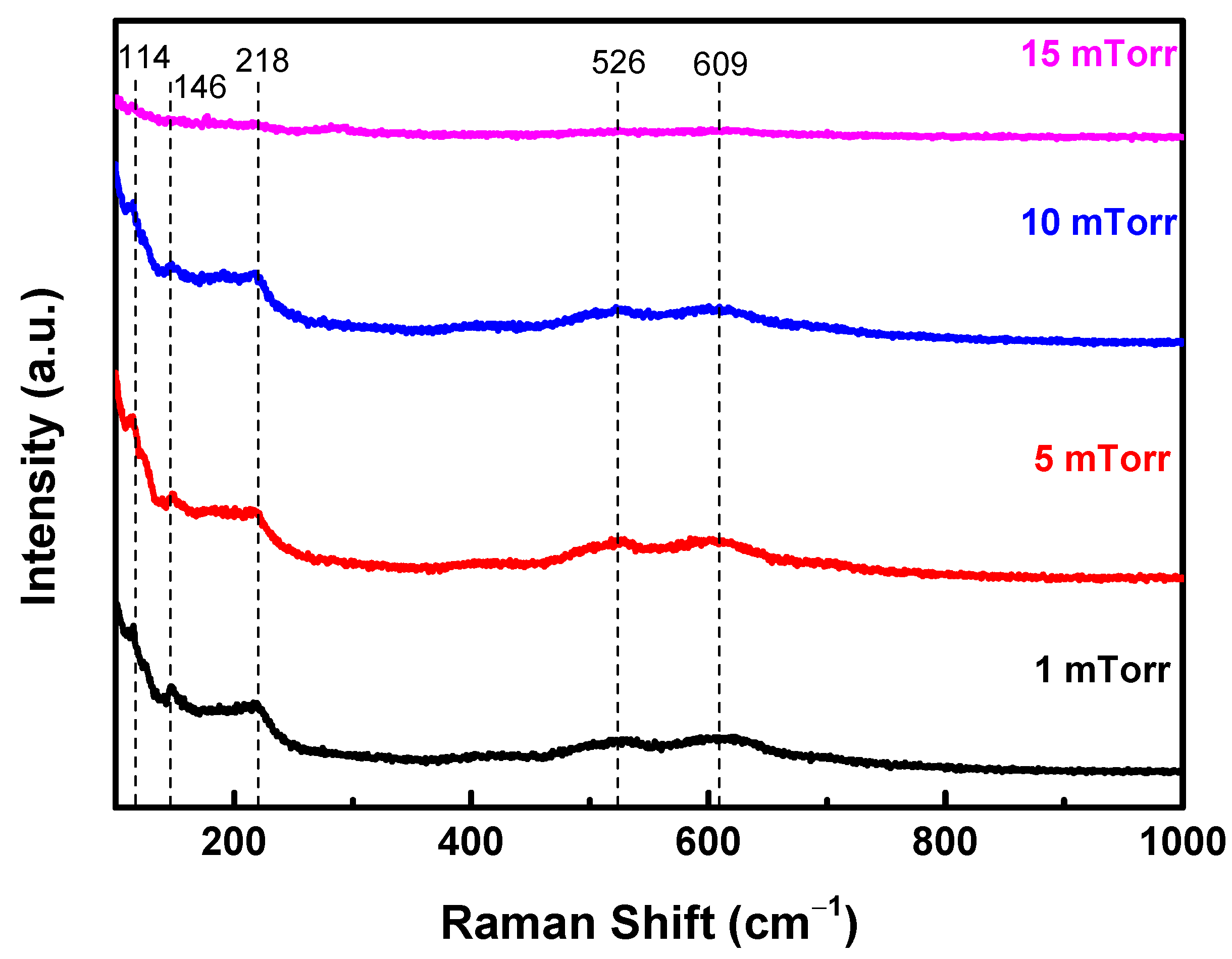
3.1. Structural Analysis of the Cu2O Thin Films

The structural properties of the Cu2O thin films deposited at various process pressures were analyzed using X-ray diffraction (XRD), and the results are presented in Figure 1. The diffraction patterns exhibit a dominant peak at approximately 36.5°, corresponding to the (111) plane of cubic Cu2O (ICDD No. 01-078-2076). This indicates that all samples predominantly crystallize in the cubic Cu2O phase with a preferred (111) orientation. At a process pressure of 5 mTorr, the (111) peak is the sharpest and most intense, signifying optimal crystallinity. The strong and narrow peak suggests the formation of larger grain sizes and fewer structural defects, which are characteristic of high-quality crystalline films. These results highlight that 5 mTorr provides the most favorable conditions for the growth of well-ordered Cu2O thin films. For the film deposited at 10 mTorr, the (111) peak remains prominent but exhibits a slight decrease in intensity and broadening compared to the 5 mTorr sample. This could indicate a reduction in crystallinity or smaller grain sizes, potentially caused by increased scattering effects during film growth at higher pressures [16]. However, the peak’s consistent position at 36.5° still confirms the stability of the cubic Cu2O phase at this pressure. At 15 mTorr, a further decrease in the intensity and broadening of the (111) peak is observed, suggesting a deterioration in crystallinity. The reduced intensity might also indicate a thinner film or lower film density, which could result from excessive process pressure disrupting the optimal deposition dynamics [17]. The broadening of the peak at this pressure suggests a greater prevalence of smaller grains or increased microstructural strain [18]. The additional peaks corresponding to other planes, such as (110), (200), and (220), are detected with much lower intensities, further confirming that the (111) plane is the dominant orientation in all samples. Importantly, no additional peaks associated with secondary phases (e.g., CuO or Cu4O3) were observed, indicating the films are composed entirely of the Cu2O phase under the tested deposition conditions. These results demonstrate that process pressure has a significant influence on the structural properties of the Cu2O thin films. The 5 mTorr sample exhibits superior crystallinity with a sharp and intense (111) peak, while higher pressures lead to decreased crystallinity and potentially smaller grain sizes. The crystalline grain sizes were calculated using the following Scherrer equation based on the XRD peak broadening data [19]:
D = K λ β cos θ
where D is the grain size, K is the shape factor (typically 0.9), λ is the X-ray wavelength (1.5406 Å), β is the full width at half maximum (FWHM) of the peak, and θ is the Bragg angle. The grain size results in Table 1 reveal a clear trend: the grain size is largest at a process pressure of 5 mTorr (36.4 nm) and decreases at both lower and higher process pressures. This supports the conclusion that process pressure significantly influences crystallite size, with lower pressures resulting in larger grains and higher pressures leading to smaller grains. These findings deepen our understanding of the structural properties of Cu2O thin films under various deposition conditions, highlighting the importance of optimizing process pressure to tailor the structural quality of Cu2O films for specific applications.
The phase composition and crystallinity of the Cu2O thin films deposited under various process pressures were investigated using Raman spectroscopy, as shown in Figure 2. The Raman spectra display characteristic peaks at approximately 114 cm−1, 146 cm−1, 218 cm−1, 526 cm−1, and 609 cm−1, which are attributed to the vibrational modes of the cubic Cu2O phase [20,21]. The consistent observation of these peaks across all samples confirms that the Cu2O phase is predominantly maintained under the tested deposition conditions. At a process pressure of 5 mTorr, the Raman spectrum exhibits sharp and intense peaks at 114 cm−1 and 146 cm−1, indicating improved crystallinity at this pressure. The moderate intensity of the 609 cm−1 peak further corroborates the presence of well-ordered Cu2O with good structural integrity. These results align with the XRD data, which also demonstrated optimal crystallinity at 5 mTorr. The 10 mTorr sample shows the strongest Raman peaks overall, particularly at 609 cm−1, which is associated with the Cu2O vibrational mode [20]. The high intensity and sharpness of this peak indicate superior crystallinity and enhanced structural ordering compared to the other samples. This suggests that 10 mTorr represents a favorable condition for achieving high-quality Cu2O films with excellent phase purity. At 15 mTorr, the Raman signal weakens significantly, with broader and less intense peaks observed across the spectrum. This reduction in peak intensity suggests a decrease in crystallinity, which may be attributed to suboptimal growth conditions at higher pressures. Additionally, the weaker signals might indicate thinner films or increased microstructural disorder, further corroborating the XRD results.
Notably, no significant peaks were observed in the range of 280–290 cm−1, which are characteristic of CuO, confirming the absence of CuO in the deposited films [22]. The dominant Raman peaks at 114 cm−1, 146 cm−1, and 609 cm−1 are consistent with the Cu2O phase, indicating that the films primarily consist of Cu2O under all deposition pressures. Overall, the Raman analysis demonstrates that process pressure has a profound effect on the structural quality of Cu2O thin films. While the 5 mTorr sample shows good crystallinity, the 10 mTorr sample exhibits the best structural properties, as evidenced by the sharp and intense Raman peaks. In contrast, the 15 mTorr sample shows diminished crystallinity, highlighting the importance of optimizing deposition pressure to achieve high-quality Cu2O thin films.

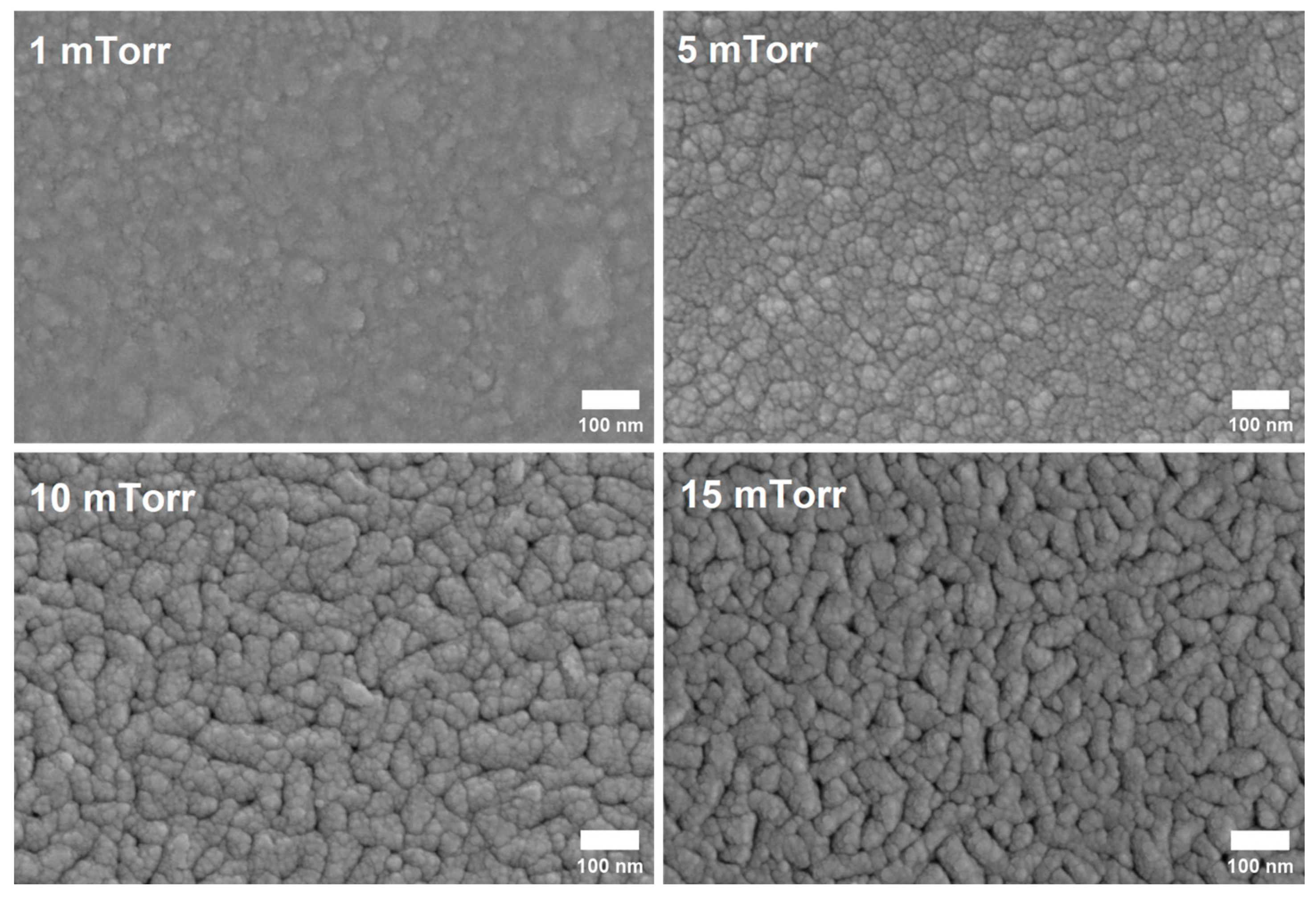
3.2. Morphological Analysis of the Cu2O Thin Films

The surface morphologies of the Cu2O thin films deposited at different process pressures were analyzed using field-emission scanning electron microscopy (FE-SEM), and the results are presented in Figure 3. The micrographs reveal significant variations in the surface morphology and grain structure depending on the deposition pressure. At 1 mTorr, the surface appears smooth with poorly defined grains, indicating a lack of well-developed crystallinity and a possible dominance of amorphous or nanocrystalline structures. The minimal grain boundaries observed suggest limited nucleation and grain growth under low-pressure conditions, likely due to insufficient energy and reduced ion bombardment during deposition [23]. At 5 mTorr, the film exhibits well-defined grains with increased size and better uniformity compared to 1 mTorr. The improved surface morphology at this pressure is consistent with enhanced nucleation and grain growth, resulting in more crystalline films [24]. This supports the XRD and Raman results, which also indicate optimal crystallinity at this pressure. The 10 mTorr sample shows larger grains with a compact and densely packed structure. The pronounced grain boundaries and increased grain size suggest that this pressure facilitates more significant grain coalescence and growth. This morphology aligns with the sharp and intense (111) peak observed in the XRD results, further indicating excellent crystallinity at 10 mTorr. In contrast, the 15 mTorr sample reveals irregularly shaped and larger grains with more porous regions, indicating a disruption in uniform grain growth. This could result from excessive scattering and reduced kinetic energy of the sputtered particles at higher pressures, leading to less uniform deposition and reduced structural integrity [25].
Overall, the FE-SEM analysis demonstrates that the deposition pressure significantly affects the surface morphology and grain structure of Cu2O thin films. The 5 mTorr and 10 mTorr samples exhibit the most uniform and well-defined grains, with the 10 mTorr sample showing the best overall grain size and packing density. These findings highlight the critical role of process pressure in tailoring the morphological properties of Cu2O thin films for specific applications. Furthermore, by integrating insights from our previous studies on the effects of substrate temperature and oxygen flow rate, this research provides a comprehensive understanding of how key deposition parameters—such as process pressure, temperature, and oxygen flow rate—work synergistically to optimize the properties of Cu2O thin films [26,27].

3.3. Compositional Analysis of the Cu2O Thin Films

The chemical composition and bonding states of the Cu2O thin films deposited under different process pressures were analyzed using X-ray photoelectron spectroscopy (XPS). The survey spectra, presented in Figure 4a, confirm the presence of copper (Cu), oxygen (O), and minor carbon (C) in all samples. The Cu 2p and O 1s peaks were examined in greater detail to investigate the oxidation states of copper and the chemical environment of oxygen in the films. The Cu 2p spectra, shown in Figure 4b, display two primary peaks at approximately 933 eV and 953 eV, corresponding to the Cu 2p3/2 and Cu 2p1/2 binding energies, respectively [28]. These peaks are characteristic of Cu(I) in Cu2O, with no observable satellite peaks typically associated with Cu(II) species such as CuO. This confirms that the films are predominantly composed of the Cu2O phase, regardless of the process pressure. Furthermore, the consistent intensity of the Cu 2p peaks across all samples suggests that the copper content remains stable under various deposition conditions [29]. The O 1s spectra, shown in Figure 4c, reveal a single dominant peak centered at approximately 530.2 eV, which corresponds to oxygen bonded within the Cu2O lattice. No additional peaks were observed in the O 1s region, indicating the absence of significant secondary oxygen species such as hydroxides or CuO [30]. A slight broadening of the O 1s peak at higher process pressures, such as 15 mTorr, may suggest an increase in surface oxidation or minor incorporation of impurities. However, the overall consistency in the O 1s peak position across all pressures reinforces the conclusion that the primary oxygen bonding state is derived from the Cu2O structure.
The XPS analysis demonstrates that the Cu2O phase is preserved across all deposition pressures, with no evidence of significant secondary phase formation such as CuO. While the chemical composition remains stable, slight variations in peak intensities and widths indicate that the process pressure may subtly affect the surface chemistry and microstructural characteristics of the films. These findings align well with the results of the structural and morphological analyses, further supporting the stability and phase purity of the Cu2O thin films under different deposition conditions.

3.4. Optical Analysis of the Cu2O Thin Film

The optical properties of the Cu2O thin films deposited under various process pressures were analyzed using UV-Vis-NIR spectroscopy, focusing on transmittance and optical band gap (Eg) characteristics. The transmittance spectra and Tauc plots reveal a clear relationship between process pressure and the films’ optical behavior. The transmittance spectra, shown in Figure 5a, demonstrate that the transparency of the thin films varies significantly with deposition pressure. At 1 mTorr, the thin film exhibits the lowest transmittance, with a maximum of approximately 65% in the near-infrared (NIR) region. This reduced transparency suggests that the film may exhibit increased surface roughness, leading to higher light scattering. At 5 mTorr, the transmittance improves significantly, reaching up to 85% in the NIR range. This enhancement reflects better film uniformity and reduced scattering losses, aligning with the superior crystallinity and phase purity observed in the XRD and Raman analyses. The film deposited at 10 mTorr maintains relatively high transmittance, peaking at around 82% in the NIR region. This indicates that the film retains good optical quality and uniformity; although, the slight reduction in transmittance compared to the 5 mTorr sample may be attributed to increased oxygen incorporation, as suggested by the XPS results. At 15 mTorr, the transmittance reaches the highest values, with a maximum of approximately 90% in the NIR range. This suggests that the film at this pressure exhibits reduced surface irregularities, resulting in minimal light scattering. However, the increase in transparency at higher pressures is accompanied by a slight increase in band gap energy, suggesting potential structural or compositional changes such as increased oxygen content or the formation of minor defects.
A protrusion observed at approximately 850 nm in Figure 5a can be attributed to interference effects caused by optical path differences at the interface between the Cu2O thin film and the soda-lime glass substrate [31,32]. This phenomenon arises from the refractive index mismatch between the Cu2O film (n ≈ 2.6) and the substrate, leading to constructive interference at specific wavelengths [15]. Such interference effects are common in transparent thin films and produce periodic oscillations in the transmittance spectra. The observed protrusion corresponds to one of these constructive interference points and does not influence the intrinsic optical properties of the Cu2O thin films. The interference fringes observed in Figure 5a were analyzed to estimate the thickness of the Cu2O thin films. The thickness (d) was calculated using the following equation [33]:
d = m λ 1 λ 2 2 ( λ 1 n 2 λ 2 n 1 )
where m is the order of interference (assumed as m = 1), λ1 and λ2 are the wavelengths of two adjacent maxima (or minima) in the interference fringes, and n is the refractive index of the Cu2O thin film (n = 2.705, based on values in the literature) [19]. The calculated film thickness values were 369.7 nm for 1 mTorr, 457.5 nm for 5 mTorr, 495.2 nm for 10 mTorr, and 443.6 nm for 15 mTorr. These results demonstrate a clear correlation between process pressure and film thickness. Thicker films were observed at 5 mTorr and 10 mTorr, which correspond to the improved optical characteristics, as reflected in the transmittance spectra and band gap values. In contrast, the reduced film thickness at 15 mTorr explains the higher transmittance observed at this pressure. This analysis highlights the relationship between process pressure, film thickness, and the resulting optical properties of Cu2O thin films.
The Tauc plots, shown in Figure 5b, provide further insight into the optical band gap of the films. At 1 mTorr, the band gap energy is 2.34 eV, which is consistent with the reported range for Cu2O (2.1–2.6 eV) [34]. This value indicates that the film retains the intrinsic optical properties of Cu2O but may exhibit slightly reduced crystallinity compared to the films deposited at higher pressures. At 5 mTorr, the band gap energy increases to 2.41 eV, suggesting improved structural and optical properties, which is consistent with the enhanced crystallinity and phase quality observed in the other analyses. The 10 mTorr sample exhibits a band gap energy of 2.38 eV, indicating that the film maintains stable structural characteristics and optical properties typical of Cu2O. At 15 mTorr, the band gap energy further increases to 2.43 eV, the highest among all samples. This increase may be attributed to changes in film density or the incorporation of additional oxygen, which could introduce slight structural distortions or defect states [35]. The band gap calculation was performed using the linear portion of the absorption curve, specifically outside the wavelength range affected by interference fringes, to ensure accuracy. This method eliminated any influence of oscillatory behavior on the band gap edge determination. Furthermore, the obtained band gap values were cross-verified with those reported in the literature for Cu2O thin films deposited under similar conditions. The calculated band gap values in this study ranged from 2.34 eV to 2.43 eV, aligning well with the established range of 2.1–2.7 eV for Cu2O thin films, confirming our analysis’s reliability. These results demonstrate that the interference fringes did not significantly impact the accuracy of the band gap determination and that the values obtained in this study accurately reflect the intrinsic optical properties of the Cu2O thin films [36,37,38].
The optical analysis reveals that deposition pressure significantly affects both the transmittance and optical band gap of Cu2O thin films. The films deposited at 5 mTorr and 10 mTorr exhibit the best balance between high transparency and optimal band gap energy, making them the most suitable for applications requiring high-quality Cu2O thin films. Conversely, the 1 mTorr sample shows reduced optical performance, while the 15 mTorr sample demonstrates the highest transparency but with potential trade-offs in band gap stability and structural integrity.

4. Conclusions

In this study, Cu2O thin films were successfully deposited on soda-lime glass substrates using RF magnetron sputtering under various process pressures, and their structural, morphological, compositional, and optical properties were systematically analyzed. The results demonstrate that process pressure plays a crucial role in tailoring the properties of Cu2O thin films, directly impacting their potential applicability in optoelectronic and photovoltaic devices. X-ray diffraction (XRD) analysis revealed that the films predominantly crystallized in the cubic Cu2O phase with a strong (111) preferential orientation. The crystallinity was found to be optimal at 5 mTorr, with a sharp and intense (111) peak, while higher pressures (10 mTorr and 15 mTorr) resulted in slightly broader peaks, indicating reduced crystallinity or smaller grain sizes. At 1 mTorr, the film showed significantly weaker XRD peaks, suggesting poor structural order. Raman spectroscopy confirmed the predominance of Cu2O across all samples, with characteristic vibrational modes observed at 114 cm−1, 146 cm−1, and 609 cm−1. At 5 mTorr and 10 mTorr, the Raman spectra exhibited sharper and more intense peaks, highlighting improved crystallinity and phase purity at these pressures. Conversely, the 1 mTorr and 15 mTorr samples showed weaker and broader peaks, which is consistent with reduced structural quality. Field-emission scanning electron microscopy (FE-SEM) revealed significant changes in surface morphology with process pressure. The 1 mTorr film displayed poorly defined grains and a relatively smooth surface, while the 5 mTorr and 10 mTorr films exhibited well-defined, densely packed grains, reflecting improved nucleation and growth under these conditions. At 15 mTorr, the grains became irregular and coarser, indicating that excessive pressure may disrupt uniform growth. X-ray photoelectron spectroscopy (XPS) confirmed the presence of Cu(I) in the Cu2O films, with no significant secondary phases such as CuO detected. The Cu 2p and O 1s peaks remained consistent across all pressures, suggesting stable chemical composition. However, slight broadening of the O 1s peak at higher pressures indicated possible surface oxidation or increased defect states, which could influence the films’ optical properties. The optical properties, as evaluated through UV-Vis-NIR spectroscopy, showed that transmittance increased with process pressure, reaching a maximum of ~90% in the NIR range for the 15 mTorr sample. However, the optical band gap, determined from Tauc plots, exhibited a decreasing trend from 2.41 eV at 5 mTorr to 2.38 eV at 10 mTorr and 2.34 eV at 1 mTorr, before slightly increasing to 2.43 eV at 15 mTorr. The films deposited at 5 mTorr and 10 mTorr exhibited the best balance between high transparency and optimal band gap values, aligning closely with the intrinsic properties of Cu2O.
In conclusion, the process pressure significantly influences the structural, morphological, compositional, and optical properties of Cu2O thin films. The results indicate that a process pressure of 5 mTorr produces films with the best combination of crystallinity, phase purity, surface uniformity, and optical performance, making it the optimal condition for fabricating high-quality Cu2O thin films. These findings provide valuable insights for tailoring the deposition conditions of Cu2O films for applications in optoelectronic devices, solar cells, and other functional materials.

Author Contributions

Conceptualization, J.P. and D.H.; methodology, Y.-G.S. and C.-S.S.; validation, J.P. and D.H.; formal analysis, J.P. and C.-S.S.; investigation, J.P. and D.H.; resources, C.-S.S. and D.H.; data curation, J.P.; writing—original draft preparation, J.P.; writing—review and editing, Y.-G.S. and D.H.; visualization, J.P. and D.H.; supervision, Y.-G.S. and D.H.; project administration, D.H.; funding acquisition, C.-S.S. and D.H. All authors have read and agreed to the published version of the manuscript.

Funding

This work was supported by the National Research Foundation of Korea (NRF) grant funded by the Korean government (MSIT) (No. NRF-2018R1A5A1025594) and was supported by “Regional Innovation Strategy (RIS)” through the National Research Foundation of Korea (NRF) funded by the Ministry of Education (MOE) (No. 2023RIS-007).

Data Availability Statement

The data are contained within the article.

Conflicts of Interest

The authors declare no conflicts of interest.

References

  1. Sekkat, A.; Liedke, M.O.; Nguyen, V.H.; Butterling, M.; Baiutti, F.; Sirvent Veru, J.D.; Weber, M.; Rapenne, L.; Bellet, D.; Chichignoud, G.; et al. Chemical deposition of Cu2O films with ultra-low resistivity: Correlation with the defect landscape. Nat. Commun. 2022, 13, 5322. [Google Scholar] [CrossRef]
  2. Lee, J.H.; Kim, J.; Jin, M.; Na, H.-J.; Lee, H.; Im, C.; Kim, Y.S. Cu2O p-type Thin-Film Transistors with Enhanced Switching Characteristics for CMOS Logic Circuit by Controlling Deposition Condition and Annealing in the N2 Atmosphere. ACS Appl. Electron. Mater. 2023, 5, 1123–1130. [Google Scholar] [CrossRef]
  3. Liu, K.; Duan, Y.-F.; Lv, D.; Wu, H.-B.; Qin, L.-X.; Shi, L.-W.; Tang, G. Pressure-Induced Cubic-to-Hexagonal Phase Transition in Cu2O. Chin. Phys. Lett. 2014, 31, 117701. [Google Scholar] [CrossRef]
  4. Deuermeier, J.; Gassmann, J.; Brötz, J.; Klein, A. Reactive magnetron sputtering of Cu2O: Dependence on oxygen pressure and interface formation with indium tin oxide. J. Appl. Phys. 2011, 109, 113704. [Google Scholar] [CrossRef]
  5. Cortona, P.; Mebarki, M. Cu2O behavior under pressure: An ab initio study. J. Phys. Condens. Matter 2011, 23, 045502. [Google Scholar] [CrossRef]
  6. Sekkat, A.; Nguyen, V.H.; Masse de La Huerta, C.A.; Rapenne, L.; Bellet, D.; Kaminski-Cachopo, A.; Chichignoud, G.; Muñoz-Rojas, D. Open-air printing of Cu2O thin films with high hole mobility for semitransparent solar harvesters. Commun. Mater. 2021, 2, 78. [Google Scholar] [CrossRef]
  7. Wang, C.; Tissot, H.; Escudero, C.; Pérez-Dieste, V.; Stacchiola, D.; Weissenrieder, J. Redox properties of Cu2O(100) and (111) surfaces. J. Phys. Chem. C 2018, 122, 28684–28691. [Google Scholar] [CrossRef]
  8. Altindemir, G.; Gumus, C. Cu2O thin films prepared by using four different copper salts at a low temperature: An investigation of their physical properties. Mater. Sci. Semicond. Process 2020, 107, 104805. [Google Scholar] [CrossRef]
  9. Iivonen, T.; Heikkila, M.J.; Popov, G.; Nieminen, H.E.; Kaipio, M.; Kemell, M.; Mattinen, M.; Meinander, K.; Mizohata, K.; Raisanen, J.; et al. Atomic Layer Deposition of Photoconductive Cu2O Thin Films. ACS Omega 2019, 4, 11205–11214. [Google Scholar] [CrossRef] [PubMed]
  10. Khan, I.A.; Hussain, S.A.; Nadeem, A.S.; Saleem, M.; Hassnain, A.; Ahmad, R. Role of Oxygen Pressure on the Surface Properties of Polycrystalline Cu2O Films Deposited by Thermal Evaporator. Mater. Phys. Chem. 2019, 1, 14. [Google Scholar] [CrossRef]
  11. Dey, A.; Chandrabose, G.; Damptey, L.A.O.; Erakulan, E.S.; Thapa, R.; Zhuk, S.; Dalapati, G.K.; Ramakrishna, S.; Braithwaite, N.S.J.; Shirzadi, A.; et al. Cu2O/CuO heterojunction catalysts through atmospheric pressure plasma induced defect passivation. Appl. Surf. Sci. 2021, 541, 148571. [Google Scholar] [CrossRef]
  12. Umar, M.; Swinkels, M.Y.; De Luca, M.; Fasolato, C.; Moser, L.; Gadea, G.; Marot, L.; Glatzel, T.; Zardo, I. Morphological and stoichiometric optimization of Cu2O thin films by deposition conditions and post-growth annealing. Thin Solid. Film. 2021, 732, 138763. [Google Scholar] [CrossRef]
  13. Nitta, R.; Taguchi, R.; Kubota, Y.; Kishi, T.; Shishido, A.; Matsushita, N. Novel Bending Sensor Based on a Solution-Processed Cu2O Film with High Resolution Covering a Wide Curvature Range. ACS Omega 2021, 6, 32647–32654. [Google Scholar] [CrossRef] [PubMed]
  14. Lee, H.S.; Yang, M.Y. The effect of negative pressure aging on the aggregation of Cu2O nanoparticles and its application to laser induced copper electrode fabrication. Phys. Chem. Chem. Phys. 2015, 17, 4360–4366. [Google Scholar] [CrossRef] [PubMed]
  15. Ait Hssi, A.; Atourki, L.; Labchir, N.; Ouafi, M.; Abouabassi, K.; Elfanaoui, A.; Ihlal, A.; Bouabid, K. Optical and dielectric properties of electrochemically deposited p-Cu2O films. Mater. Res. Express 2020, 7, 016424. [Google Scholar] [CrossRef]
  16. Wei, L.; Leng, C. Sputtering pressure effects on microstructure and grain orientation distribution in FePt thin films. J. Mater. Sci. Mater. Electron. 2017, 28, 5634–5640. [Google Scholar]
  17. Yue, T.; Lee, H.Y.; Lee, H.; Lee, Y.H. Effect of Sputtering Pressure on the Nanostructure and Residual Stress of Thin-Film YSZ Electrolyte. Sustainability 2022, 14, 9704. [Google Scholar] [CrossRef]
  18. Bindu, P.; Thomas, S. Estimation of lattice strain in ZnO nanoparticles: X-ray peak profile analysis. J. Theor. Appl. Phys. 2014, 8, 258–264. [Google Scholar] [CrossRef]
  19. Swanepoel, R. Determining refractive index and thickness of thin films from wavelength measurements only. J. Opt. Soc. Am. A 1985, 2, 1339–1343. [Google Scholar] [CrossRef]
  20. Choudhary, S.; Sarma, J.V.; Pande, S.; Ababou-Girard, S.; Turban, P.; Lepine, B.; Gangopadhyay, S. Oxidation mechanism of thin Cu films: A gateway towards the formation of single oxide phase. AIP Adv. 2018, 8, 055114. [Google Scholar] [CrossRef]
  21. Daniel, A.F.; Alekha, T.; Sugandha, S.; Prerna, S.; Amodini, M.; Somnath, D.; Rajesh, K.; Kamal, K.K. Tunable optical and electrical properties of p-type Cu2O thin films. J. Mater. Sci. Mater. Electron. 2021, 32, 11158–11172. [Google Scholar]
  22. Goldstein, H.F.; Kim, D.-s.; Yu, P.Y.; Bournet, L.C. Raman study of Cuo single crystals. Phys. Rev. B 1990, 41, 7192–7197. [Google Scholar] [CrossRef]
  23. Brian, W.K.; David, G.C.; Petrov, I.; Greene, J.E. Effects of high-flux low-energy ion bombardment on the low-temperature growth morphology of TiN(001) epitaxial layers. AIP Adv. 2011, 1, 042117. [Google Scholar]
  24. Sriram, K.; Yaswanth, S.P.; Peddiraju, V.C.; Rohiteswar, M.; Devapriya, M.S.; Arabinda, H.; Chandrasekhar, M. Deposition pressure-controlled phase tailoring and stability of β-W for spintronic applications. J. Appl. Phys. 2024, 136, 045302. [Google Scholar] [CrossRef]
  25. Lan, Z.; Yiping, W.; Hua, Z.; Minghao, L.; Randall, L.; Headrick, R.L. Pressure-dependent transition from atoms to nanoparticles in magnetron sputtering: Effect on WSi2 film roughness and stress. Phys. Rev. B 2010, 82, 075408. [Google Scholar]
  26. Kim, J.-A.; Park, J.-H.; Park, S.-G.; Son, C.-S.; Son, Y.-G.; Hwang, D.-H. Effect of Substrate Temperature on Variations in the Structural and Optical Properties of Cu2O Thin Films Deposited via RF Magnetron Sputtering. Crystals 2023, 13, 643. [Google Scholar] [CrossRef]
  27. Park, J.; Son, Y.-G.; Son, C.-S.; Hwang, D. Influence of Oxygen Flow Rate on the Phase Structures and Properties for Copper Oxide Thin Films Deposited by RF Magnetron Sputtering. Coatings 2024, 14, 930. [Google Scholar] [CrossRef]
  28. Marta, M.N.; Alessandro, G.; Antonella, G. CuO/CeO2 Nanocomposites: An XPS Study. Surf. Sci. Spectra 2009, 16, 16–26. [Google Scholar]
  29. Davide, B.; Alberto, G.; Eugenio, T. CVD Cu2O and CuO Nanosystems Characterized by XPS. Surf. Sci. Spectra 2007, 14, 41–48. [Google Scholar]
  30. Dupin, J.-C.; Danielle, G.; Philippe, V.; Alain, L. Systematic XPS studies of metal oxides, hydroxides and peroxides. Phys. Chem. Chem. Phys. 2000, 2, 1319–1324. [Google Scholar] [CrossRef]
  31. Born, M.; Wolf, E. Principles of Optics: Electromagnetic Theory of Propagation, Interference and Diffraction of Light, 7th ed.; Cambridge University Press: Cambridge, UK, 1999. [Google Scholar]
  32. Chia, C.-H.; Su, S.-H.; Hu, Y.-M.; Chiou, J.-W.; Yu, C.-C.; Jian, S.-R. Photoluminescence Characteristics of Post-annealed Cu2O Thin Films. J. Electron. Mater. 2024, 53, 7261–7270. [Google Scholar] [CrossRef]
  33. Swanepoel, R. Determination of the thickness and optical constants of amorphous silicon. J. Phps. E Sci. Instrum. 1983, 16, 1214–1222. [Google Scholar] [CrossRef]
  34. Hssi, A.A.; Atourki, L.; Labchir, N.; Ouafi, M.; Abouabassi, K.; Elfanaoui, A.; Ihlal, A.; Benmokhtar, S. High-quality Cu2O thin films via electrochemical synthesis under a variable applied potential. J. Mater. Sci. Mater. Electron. 2020, 31, 1234–1245. [Google Scholar]
  35. Rajesh, D.; Bijaya, B.; Manoj, P.; Sandip, B.; Biplab, B.; Kshama, P.; Santosh, K.T.; Kafle, B.P. Effect of Oxygen Vacancy on the Crystallinity and Optical Band Gap in Tin Oxide Thin Film. Energies 2023, 16, 2653. [Google Scholar] [CrossRef]
  36. Wang, Y.; Miska, P.; Pilloud, D.; Horwat, D.; Mücklich, F.; Pierson, J.F. Transmittance enhancement and optical band gap widening of Cu2O thin films after air annealing. J. Appl. Phys. 2014, 115, 073505. [Google Scholar] [CrossRef]
  37. Pagare, P.K.; Torane, A.P. Band gap varied cuprous oxide (Cu2O) thin films as a tool for glucose sensing. Microchim. Acta 2016, 183, 2983–2989. [Google Scholar] [CrossRef]
  38. Kaur, J.; Khanna, A.; Kumar, R.; Chandra, R. Growth and characterization of Cu2O and CuO thin films. J. Mater. Sci: Mater. Electron. 1922, 33, 16154–16166. [Google Scholar] [CrossRef]
Figure 1. XRD patterns of the Cu2O thin films deposited under various process pressures.
Crystals 15 00002 g001
Figure 2. Raman spectra of the Cu2O thin films deposited under different process pressures.
Crystals 15 00002 g002
Figure 3. FE-SEM images of the Cu2O thin films deposited under different process pressures.
Crystals 15 00002 g003
Figure 4. XPS analysis of the Cu2O thin films deposited at different process pressures: (a) survey spectra showing Cu 2p, O 1s, and C 1s peaks, (b) high-resolution Cu 2p spectra confirming the presence of Cu(I) in the Cu2O phase, and (c) O 1s spectra illustrating the oxygen bonding states in the Cu2O structure.
Crystals 15 00002 g004
Figure 5. Optical properties of the Cu2O thin films deposited under various process pressures: (a) transmittance spectra showing transparency variations and (b) Tauc plots estimating the optical band gaps.
Crystals 15 00002 g005
Table 1. Crystallite size and FWHM values of the Cu2O thin films at different process pressures calculated using the Scherrer equation.
Process Pressure
(mTorr)
FWHM
(Degree)
Crystallite Size
(nm)
10.5815.2
50.2436.4
100.4818.2
150.969.11
Disclaimer/Publisher’s Note: The statements, opinions and data contained in all publications are solely those of the individual author(s) and contributor(s) and not of MDPI and/or the editor(s). MDPI and/or the editor(s) disclaim responsibility for any injury to people or property resulting from any ideas, methods, instructions or products referred to in the content.

