
Anion and Cation Co-Doping of NiO for Transparent Photovoltaics and Smart Window Applications

 , , , ,
Abstract
1. Introduction
2. Materials and Methods
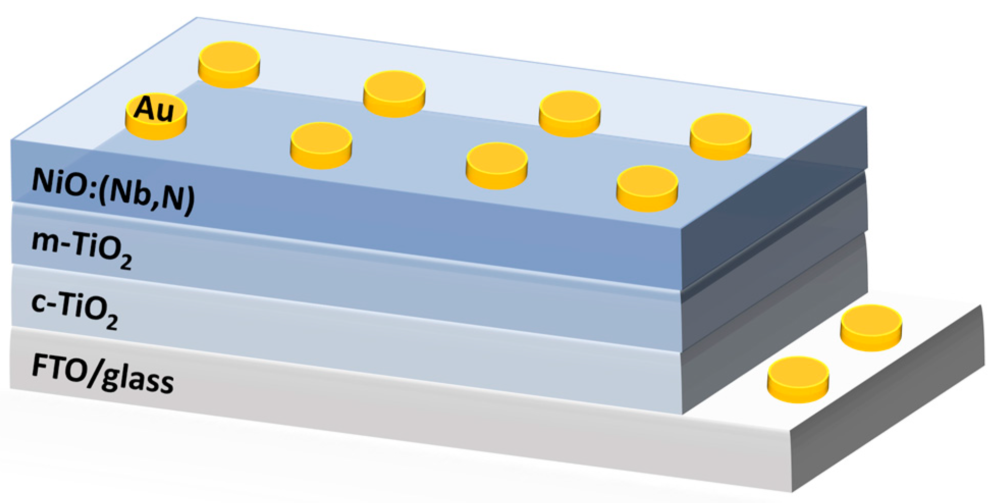
2.1. Thin Films Deposition and Device Fabrication
2.2. Characterization Methods of Thin Films and Devices
3. Results and Discussion
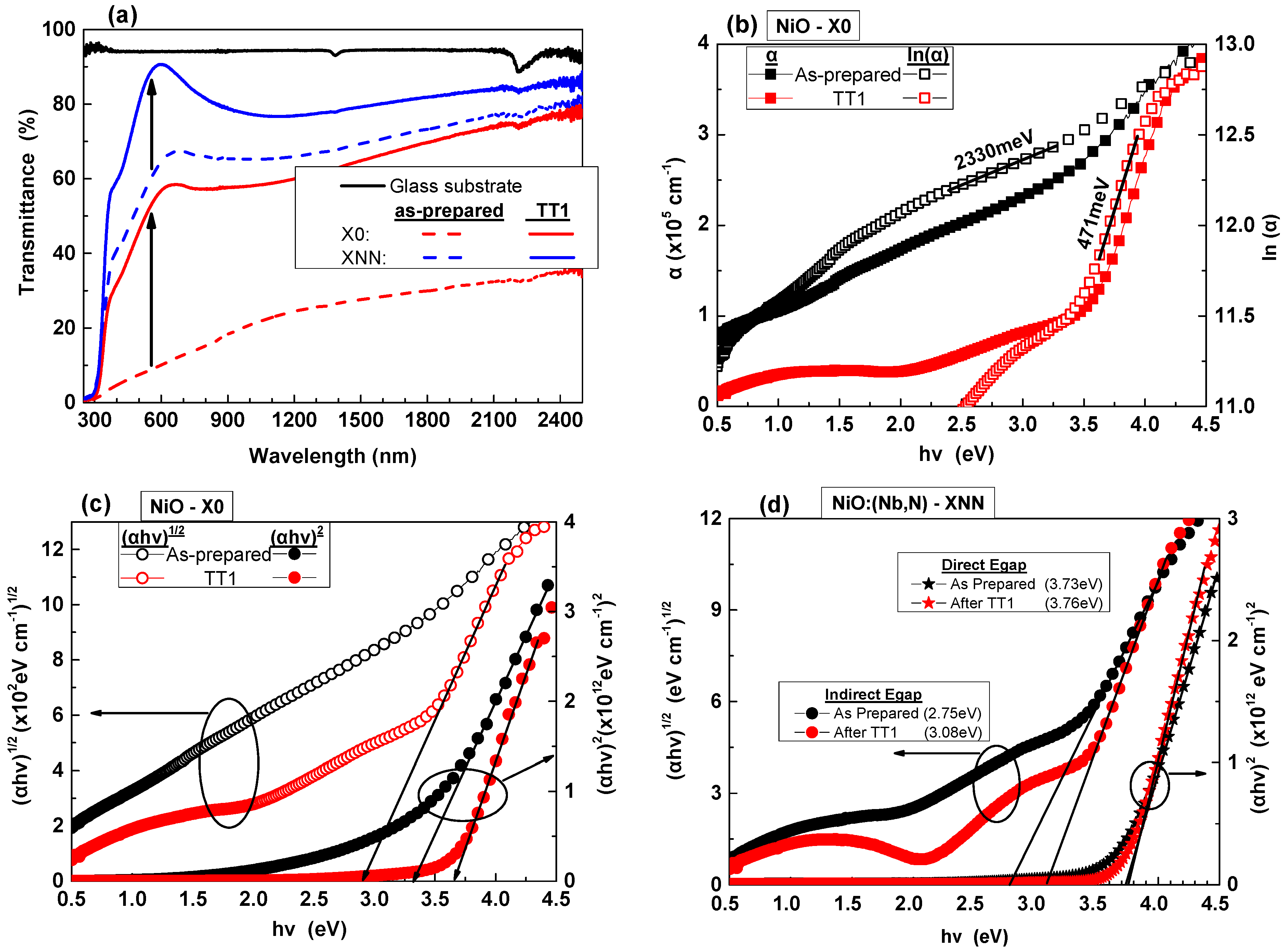
3.1. Thin Films Properties
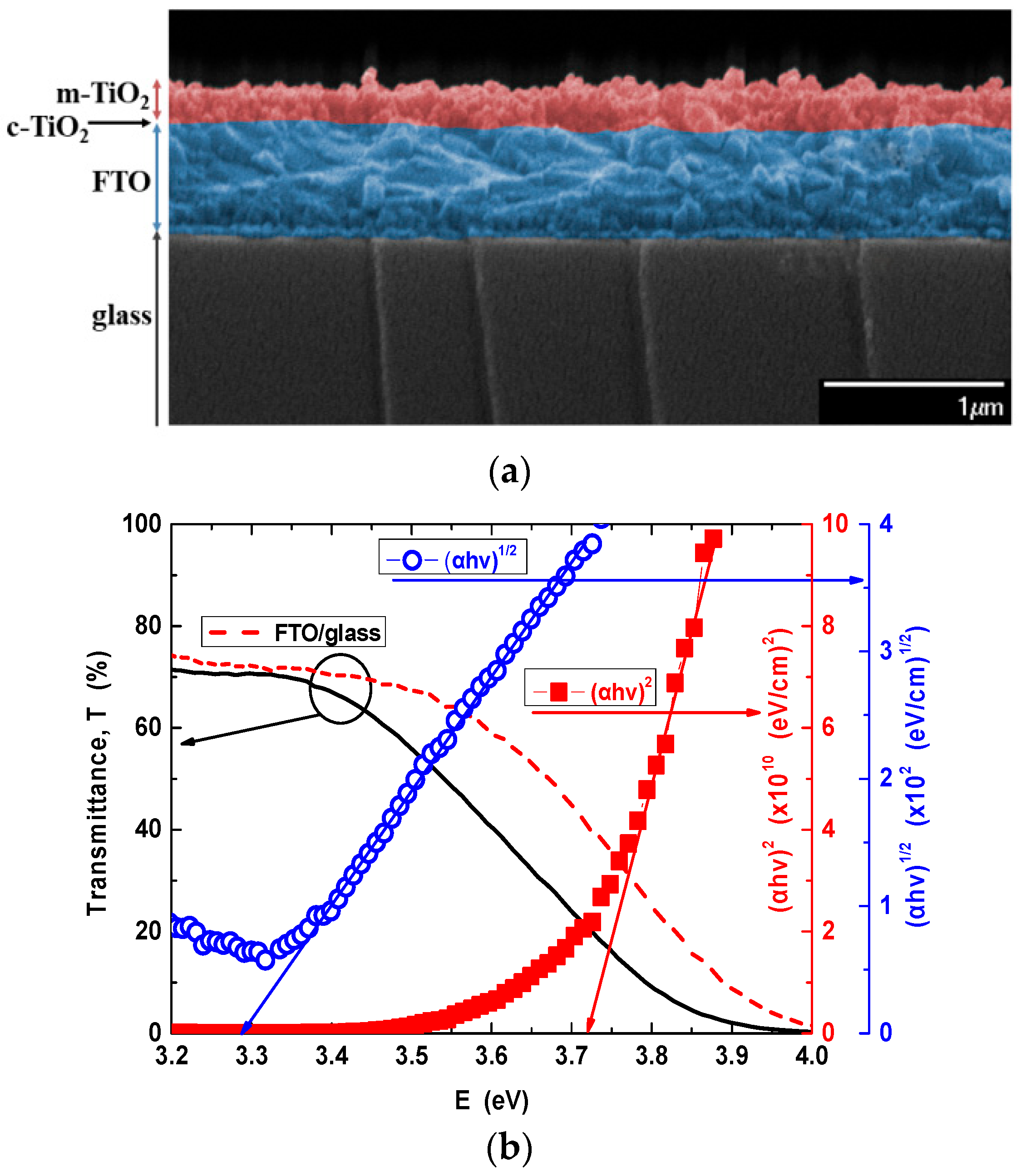
3.1.1. Properties of TiO2 Layer
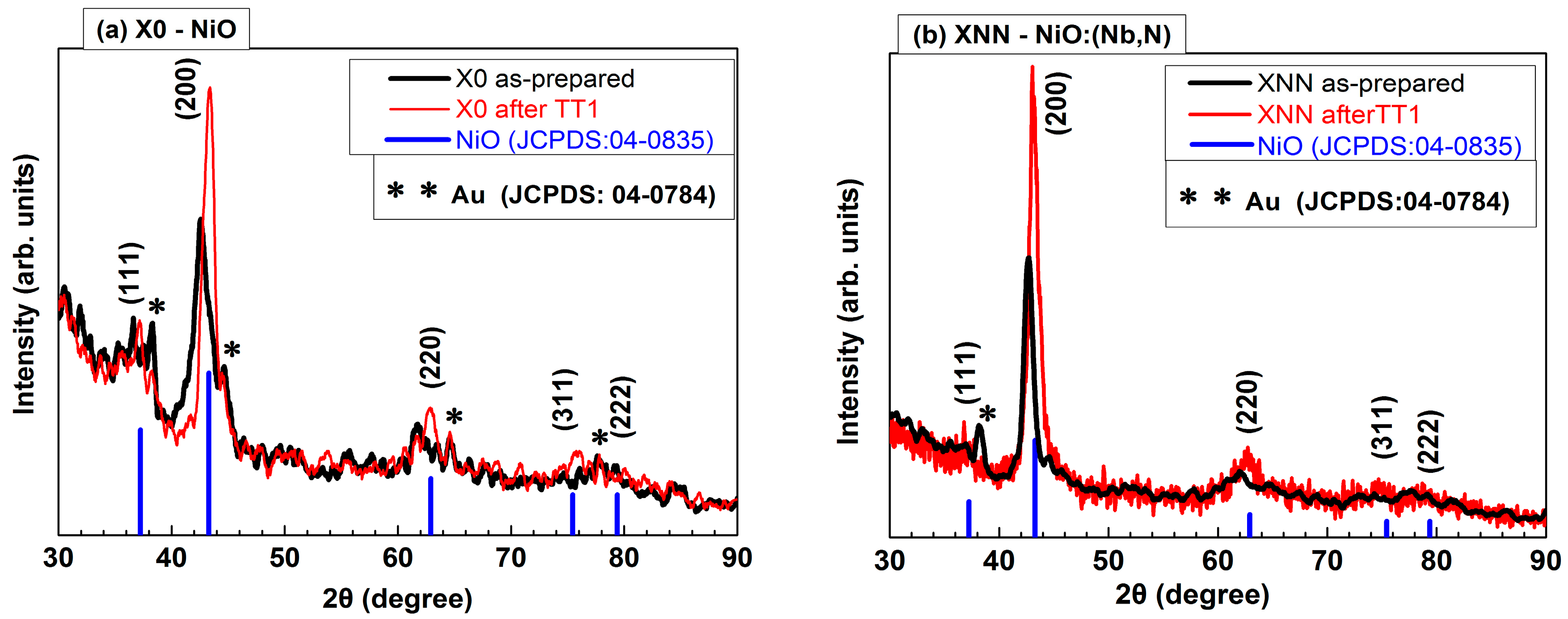
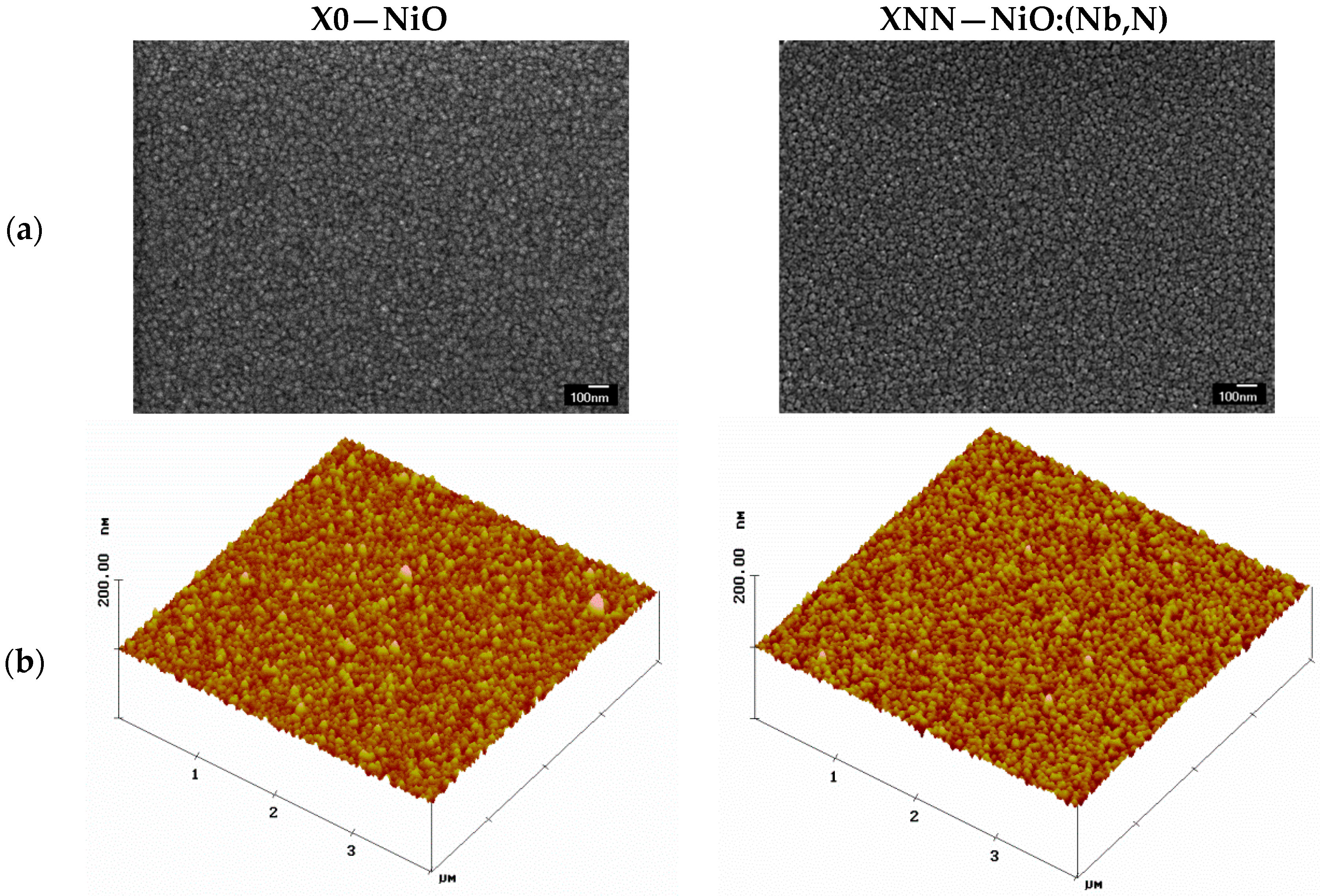
3.1.2. Properties of NiO and NiO:(Nb,N) Thin Films
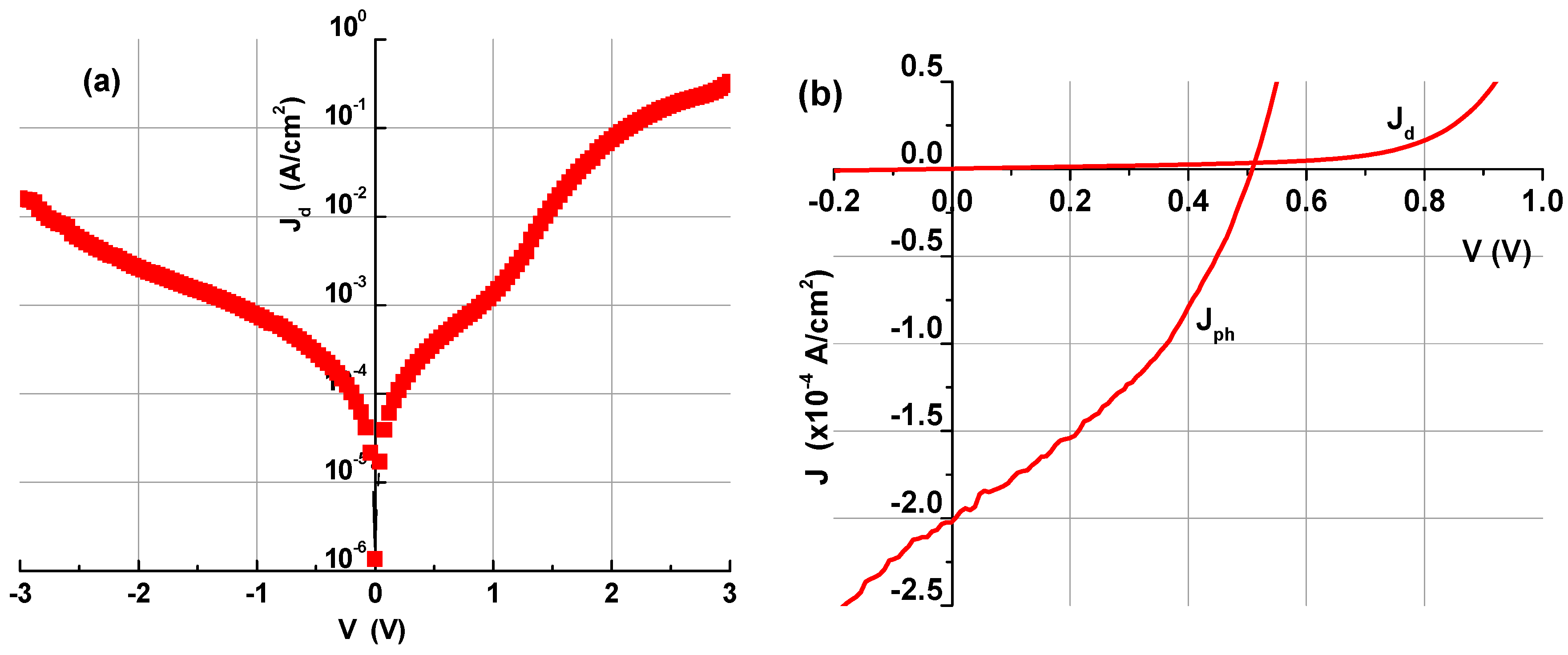
3.2. Properties of NiO:(Nb,N)/TiO2 Heterostructure
4. Conclusions
Supplementary Materials
Author Contributions
Funding
Data Availability Statement
Acknowledgments
Conflicts of Interest
References
- Lemmet, S. Buildings and Climate Change: Summary for Decision-Makers Sustainable Buildings & Climate Initiative; United Nations Environmental Programme: Paris, France, 2009; pp. 1–62. [Google Scholar]
- Yang, L.; Yan, H.; Lam, J.C. Thermal comfort and building energy consumption implications—A review. Appl. Energy 2014, 115, 164–173. [Google Scholar] [CrossRef]
- Wang, Z.; Wang, X.; Cong, S.; Geng, F.; Zhao, Z. Fusing electrochromic technology with other advanced technologies: A new roadmap for future development. Mater. Sci. Eng. R 2020, 140, 100524. [Google Scholar] [CrossRef]
- Lunt, R.R. Theoretical limits for visibly transparent photovoltaics. Appl. Phys. Lett. 2012, 101, 043902. [Google Scholar] [CrossRef]
- Ukoba, K.O.; Inambao, F.L.; Eloka-Eboka, A.C. Fabrication of affordable and sustainable solar cells using NiO/TiO2 P-N heterojunction. Int. J. Photoenergy 2018, 7, 6062390. [Google Scholar] [CrossRef]
- Abbas, S.; Kim, J. All-metal oxide transparent photodetector for broad responses. Sens. Actuators A 2020, 303, 111835. [Google Scholar] [CrossRef]
- Aivalioti, C.; Manidakis, E.G.; Pelekanos, N.T.; Androulidaki, M.; Tsagaraki, K.; Viskadourakis, Z.; Spanakis, E.; Aperathitis, E. Niobium-doped NiO as p-type nanostructured layer for transparent photovoltaics. Thin Solid Film. 2023, 778, 139910. [Google Scholar] [CrossRef]
- Xu, J.; Cao, R.; Shi, S.; Li, L.; Zhu, K.; Su, Y. Self-powered ultraviolet photodetectors based on match like quasi one- dimensional n-TiO2/p-NiO core-shell heterojunction arrays with NiO layer sputtered at different power. J. Alloys Compd. 2022, 928, 167126. [Google Scholar] [CrossRef]
- Kumar, N.; Patel, M.; Nguyen, T.T.; Kim, S.; Kim, J. Effect of TiO2 layer thickness of TiO2/NiO transparent photovoltaics. Prog. Photovolt. Res. Appl. 2021, 29, 943–952. [Google Scholar] [CrossRef]
- Klochko, N.P.; Kopach, V.R.; Tyukhov, I.I.; Zhadan, D.O.; Klepikova, K.S.; Khrypunova, G.S.; Petrushenko, S.I.; Lyubov, V.M.; Kirichenko, M.V.; Dukarov, S.V.; et al. Metal oxide heterojunction (NiO/ZnO) prepared by low temperature solution growth for UV-photodetector and semi-transparent solar cell. Sol. Energy 2018, 164, 149–159. [Google Scholar] [CrossRef]
- Nguyen, T.T.; Patel, M.; Kim, J.W.; Lee, W.; Kim, J. Functional TiO2 interlayer for all transparent metal-oxide photovoltaics. J. Alloys Compd. 2020, 816, 152602. [Google Scholar] [CrossRef]
- Grundmann, M.; Klüpfel, F.; Karsthof, R.; Schlupp, P.; Schein, F.-L.; Splith, D.; Yang, C.; Bitter, S.; von Wenckstern, H. Oxide bipolar electronics: Materials, devices and circuits. J. Phys. D Appl. Phys. 2016, 49, 213001. [Google Scholar] [CrossRef]
- Karsthof, R.; Racke, P.; von Wenckstern, H.; Grundmann, M. Semi-transparent NiO/ZnO UV photovoltaic cells. Phys. Status Solidi A 2016, 213, 30–37. [Google Scholar] [CrossRef]
- Ghosh, S.; Patel, M.; Lee, J.; Kim, J. All-Oxide Transparent Photodetector Array for Ultrafast Response through Self-Powered Excitonic Photovoltage Operation. Small 2023, 19, 2301702. [Google Scholar] [CrossRef] [PubMed]
- Hovel, H.J.; Willardson, R.K.; Beer, A.C. Solar Cells; Chapter 2, Semiconductors and Semimetals Series, 11; Academic Press: New York, NY, USA, 1976; ISBN 10: 0127521119, ISBN 13: 9780127521114. [Google Scholar]
- Patel, M.; Nguyen, T.T.; Kumar, M.; Ban, D.K.; Won, D.; Zhao, M.; Kim, J.; Kim, Y.K.; Yang, H.; Wonger, C.P. 2D layer-embedded transparent photovoltaics. Nano Energy 2020, 68, 104328. [Google Scholar] [CrossRef]
- Fu, W.; Pan, J.; Niu, J.; Fu, Y.; Xiao, G.; Wang, J.; Zheng, Y.; Li, C. A transparent photovoltaic device of NiO/MgO quantum dots/TiO2 arrays pn junction with carrier injection of MgO QDs. J. Mater. Sci. Mater. Electron. 2022, 33, 652–662. [Google Scholar] [CrossRef]
- Aivalioti, C.; Papadakis, A.; Manidakis, E.; Kayambaki, M.; Androulidaki, M.; Tsagaraki, K.; Pelekanos, N.T.; Stoumpos, C.; Modreanu, M.; Crăciun, G.; et al. Transparent All-Oxide Hybrid NiO:N/TiO2 Heterostructure for Optoelectronic Applications. Electronics 2021, 10, 988. [Google Scholar] [CrossRef]
- Aivalioti, C.; Papadakis, A.; Manidakis, E.; Kayambaki, M.; Androulidaki, M.; Tsagaraki, K.; Pelekanos, N.T.; Stoumpos, C.; Modreanu, M.; Craciun, G.; et al. An Assessment of Sputtered Nitrogen-Doped Nickel Oxide for all-Oxide Transparent Optoelectronic Applications: The Case of Hybrid NiO:N/TiO2 Heterostructure. In Recent Trends in Chemical and Material Sciences; B P International: London, UK, 2022; Volume 6, pp. 86–111, Chapter 8. [Google Scholar] [CrossRef]
- Yang, D.; Zhou, X.; Yang, R.; Yang, Z.; Yu, W.; Wang, X.; Li, C.; Liu, S.; Chang, R.P.H. Surface optimization to eliminate hysteresis for record efficiency planar perovskite solar cells. Energy Environ. Sci. 2016, 9, 3071. [Google Scholar] [CrossRef]
- Gagaoudakis, E.; Michail, G.; Kampylafka, V.; Tsagaraki, K.; Aperathitis, E.; Moschovis, K.; Binas, V.; Kiriakidis, G. Room Temperature p-Type NiO Nanostructure Thin Film Sensor for Hydrogen and Methane Detection. Sens. Lett. 2017, 15, 663–667. [Google Scholar] [CrossRef]
- Nath, D.; Singh, F.; Das, R. X-ray diffraction analysis by Williamson-Hall, Halder-Wagner and size-strain plot methods of CdSe nanoparticles- a comparative study. Mat. Chem. Phys. 2020, 239, 122021. [Google Scholar] [CrossRef]
- Pankove, J. Optical Processes in Semiconductors; Dover Publications: New York, NY, USA, 1971; p. 87, Chapter 4. [Google Scholar]
- Davis, E.A.; Mott, N.F. Conduction in non-crystalline systems V. Conductivity, optical absorption and photoconductivity in amorphous semiconductors. Philos. Mag. 1970, 22, 0903–0922. [Google Scholar] [CrossRef]
- Sze, S.M. Physics of Semiconductor Devices, 2nd ed.; John Wiley and Sons Ltd.: Hoboken, NJ, USA, 1981; ISBN 13: 978-0471098379. [Google Scholar]
- Bi, Z.; Liu, X.; Zhang, Y.; Zhang, Y.; Ma, Y.; Chen, Y.; Zhou, J.; Ruan, S. An MSM photodetector based on an InGaO/TiO2heterojunction for high-performance UV detection. Appl. Phys. Lett. 2024, 124, 022101. [Google Scholar] [CrossRef]
- Naas, L.-A.; Bouaouina, B.; Bensouici, F.; Mokeddem, K.; Abaidia, S.E. Effect of TiN thin films deposited by oblique angle sputter deposition on sol-gel coated TiO2 layers for photocatalytic applications. Thin Solid Film. 2024, 793, 140275. [Google Scholar] [CrossRef]
- Shalaan, E.; Ibrahim, E.; Al-Marzouki, F.; Al-Dossari, M. Observation of mixed types of energy gaps in some II–VI semi-conductors nanostructured films: Towards enhanced solar cell performance. Appl. Phys. A 2020, 126, 852. [Google Scholar] [CrossRef]
- Choudhury, B.; Choudhury, A. Oxygen defect dependent variation of band gap, Urbach energy and luminescence property of anatase, anatase–rutile mixed phase and of rutile phases of TiO2 nanoparticles. Phys. E 2014, 56, 364–371. [Google Scholar] [CrossRef]
- Kavan, L. Electrochemistry and band structure of semiconductors (TiO2, SnO2, ZnO): Avoiding pitfalls and textbook errors. J. Solid State Electrochem. 2024, 28, 829–845. [Google Scholar] [CrossRef]
- Mor, G.K.; Varghese, O.K.; Paulose, M.; Shankar, K.; Grimes, C.A. A review on highly ordered, vertically oriented TiO2na-notube arrays: Fabrication, material properties, and solar energy applications. Sol. Energy Mater. Sol. Cells 2006, 90, 2011–2075. [Google Scholar] [CrossRef]
- Keraudy, J.; Ferrec, A.; Richard-Plouet, M.; Hamon, J.; Goullet, A.; Jouan, P.-Y. “Nitrogen doping on NiO by reactive magne-tron sputtering: A new pathway to dynamically tune the optical and electrical properties. Appl. Surf. Sci. 2017, 409, 77–84. [Google Scholar] [CrossRef]
- Himmerlich, M.; Koufaki, M.; Ecke, G.; Mauder, C.; Cimalla, V.; Schaefer, J.A.; Kondilis, A.; Pelekanos, N.T.; Modreanu, M.; Krischok, S.; et al. Effect of Annealing on the Properties of Indium−Tin−Oxynitride Films as Ohmic Contacts for GaN-Based Optoelectronic Devices. ACS Appl. Mater. Interfaces 2009, 1, 1451–1456. [Google Scholar] [CrossRef]
- Jin, S.; Guan, W.; Tsang, C.-W.; Yan, D.Y.S.; Chan, C.-Y.; Liang, C. Enhanced Hydroconversion of Lignin-Derived Oxy-gen-Containing Compounds Over Bulk Nickel Catalysts Though Nb2O5 Modification. Catal. Lett. 2017, 147, 2215–2224. [Google Scholar] [CrossRef]
- Qiu, L.; Zhang, S.; Huang, J.; Wang, C.; Zhao, R.; Qu, F.; Wang, P.; Yang, M. Highly selective and sensitive xylene sensors based on Nb-doped NiO nanosheets. Sens. Actuators B. Chem. 2020, 308, 127520. [Google Scholar] [CrossRef]
- Hwang, J.D.; Ho, T.H. Effects of oxygen content on the structural, optical, and electrical properties of NiO films fabricated by radio-frequency magnetron sputtering. Mat. Sci. Semicond. Process. 2017, 71, 396–400. [Google Scholar] [CrossRef]
- Tian, Y.; Gong, L.; Qi, X.; Yang, Y.; Zhao, X. Effect of Substrate Temperature on the Optical and Electrical Properties of Nitrogen-Doped NiO Thin Films. Coatings 2019, 9, 634. [Google Scholar] [CrossRef]
- Peng, W.B.; Zhou, Y.J.; Xiang, G.J.; Liu, Y.; Zhang, J.H.; Zhang, J.M.; Huang, H.X.; Mei, M.Y.; Wang, H.; Zhao, Y. Preparation of AlN thin film and the impacts of AlN buffer layer on the carrier transport properties of p-NiO/n-InN heterojunction by magnetron sputtering. Mater. Sci. Semicond. Process. 2022, 141, 106417. [Google Scholar] [CrossRef]
- Lin, C.-W.; Chung, W.-C.; Zhang, Z.-D.; Hsu, M.-C. P-channel transparent thin-film transistor using physical-vapor-deposited NiO layer. Jpn. J. Appl. Phys. 2018, 57, 01AE01. [Google Scholar] [CrossRef]
- Park, S.G.; Lee, K.H.; Lee, J.-H.; Bang, G.; Kim, J.; Park, H.J.; Oh, M.S.; Lee, S.; Kim, Y.-H.; Kim, Y.-M.; et al. Improved polaronic transport under a strong Mott–Hubbard interaction in Cu substituted NiO. Inorg. Chem. Front. 2020, 7, 853–858. [Google Scholar] [CrossRef]
- Siddique, M.N.; Ahmed, A.; Tripathi, P. Enhanced optical properties of pure and Sr doped NiO nanostructures: A compre-hensive study. Optik 2019, 185, 599–608. [Google Scholar] [CrossRef]
- Zanatta, A.R. Revisiting the optical bandgap of semiconductors and the proposal of a unified methodology to its determination. Sci. Rep. 2019, 9, 11225. [Google Scholar] [CrossRef]
- Gong, H.; Chen, X.; Xu, Y.; Chen, Y.; Ren, F.; Liu, B.; Gu, S.; Zhang, R.; Ye, J. Band Alignment and Interface Recombination in NiO/β-Ga2O3 Type-II p-n Heterojunctions. IEEE Trans. Electron Devices 2020, 67, 3341–3347. [Google Scholar] [CrossRef]
- Popescu, I.; Skoufa, Z.; Heracleous, E.; Lemonidou, A.; Marcu, I.-C. A study by electrical conductivity measurements of the semiconductive and redox properties of Nb-doped NiO catalysts in correlation with the oxidative dehydrogenation of ethane. Phys. Chem. Chem. Phys. 2015, 17, 8138–8147. [Google Scholar] [CrossRef]
- Polyakov, A.Y.; Smirnov, N.B.; Shchemerov, I.V.; Vasilev, A.A.; Kochkova, A.I.; Chernykh, A.V.; Lagov, P.B.; Pavlov, Y.S.; Stolbunov, V.S.; Kulevoy, T.V.; et al. Crystal orientation dependence of deep level spectra in proton irradiated bulk β-Ga2O3. J. Appl. Phys. 2021, 130, 035701. [Google Scholar] [CrossRef]
- Karsthof, R.; von Wenckstern, H.; Zúniga-Pérez, J.; Deparis, C.; Grundmann, M. Nickel Oxide–Based Heterostructures with Large Band Offsets. Phys. Status Solidi B 2020, 257, 1900639. [Google Scholar] [CrossRef]
- Vygranenko, Y.; Wang, K.; Nathan, A. Low leakage heterostructure ultraviolet sensor. Appl. Phys. Lett. 2006, 89, 172105. [Google Scholar] [CrossRef]
- Nguyen, T.T.; Patel, M.; Kim, J. All-inorganic metal oxide transparent solar cells. Sol. Energy Mater. Sol. Cells 2020, 217, 110708. [Google Scholar] [CrossRef]
- Hwang, J.D.; Jiang, C.I.; Hwang, S.B. P-NiO/n-ZnO heterojunction photodiodes with an MgZnO/ZnO quantumwell insertion layer. Mater. Sci. Semicond. Process. 2020, 105, 104711. [Google Scholar] [CrossRef]
- Dawidowski, W.; Sciana, B.; Bielak, K.; Mikolášek, M.; Drobný, J.; Serafinczuk, J.; Lombardero, I.; Radziewicz, D.; Kijaszek, W.; Kósa, A.; et al. Analysis of Current Transport Mechanism in AP-MOVPE Grown GaAsN p-i-n Solar Cell. Energies 2021, 14, 4651. [Google Scholar] [CrossRef]
- Wang, J.; Ren, Y.; Wang, P. (Fe, F) co-doped nickel oxyhydroxide for highly efficient oxygen evolution reaction. J. Mater. Chem. A 2023, 11, 4619. [Google Scholar] [CrossRef]
- Wen, C.-K.; Xin, Y.-Q.; Chen, S.-C.; Chuang, T.-H.; Chen, P.-J.; Sun, H. Comparison of microstructural and optoelectronic properties of NiO:Cu thin films deposited by ion-beam assisted rf sputtering in different gas atmospheres. Thin Solid Film. 2019, 677, 103–108. [Google Scholar] [CrossRef]
- Raj, I.L.P.; Valanarasu, S.; Ade, R.; Bitla, Y.; Mohanraj, P.; Ganesh, V.; Yahia, I.S. Enhancing the ultraviolet photosensingproperties of nickel oxide thin films by Zn–La co-doping. Ceram. Int. 2022, 48, 5026–5034. [Google Scholar] [CrossRef]
- Dong, D.; Wang, W.; Barnabe, A.; Presmanes, L.; Rougier, A.; Dong, G.; Zhang, F.; Yu, H.; He, Y.; Dia, X. Enhanced electrochromism in short wavelengths for NiO:(Li,Mg) films in full inorganic device ITO/NiO:(Li, Mg)/Ta2O5/WO3/ITO. Electrochim. Acta 2018, 263, 277–285. [Google Scholar] [CrossRef]
- Abbas, H.; Nadeem, K.; Munir, S.; Ahmed, U.; Usman, M.; Kostylev, M. Fe–Co co-doping effects on antiferromagnetic core of NiO nanoparticles. Ceram. Int. 2022, 48, 3435–3447. [Google Scholar] [CrossRef]
- Ahmed, A.A.A.; Alahsab, E.A.A.; Abdulwahab, A.M. The influence of Zn and Mg doping on the structural and optical properties of NiO nano-structures for optoelectronic applications. Results Phys. 2021, 22, 103938. [Google Scholar] [CrossRef]
- El Sayed, A.M. Exploring the morphology, optical and electrical properties of nickel oxide thin films under lead and iridium doping. Phys. B 2021, 600, 412601. [Google Scholar] [CrossRef]


| (A) m-TiO2/c-TiO2 Films | ||
|---|---|---|
| Details | Compact TiO2—c-TiO2 | Mesoporous TiO2—m-TiO2 |
| Spin-coating | HCl:C₂H₆O:C12H28O4Ti = 50µL:2.3mL:150µL | TiO2paste + C₂H₆O |
| Rounds per minute/duration (sec) | 2000/30 | 6000/30 |
| Thermal treatment | 500 °C/air/15 min | 500 °C/air/15 min |
| Thickness (nm) | 40 | 200 |
| Substrates | FTO/glass (2 mm thick glass) | c-TiO2/FTO/glass |
| (B) NiO-based films | ||
| Details | NiO—Film X0 | NiO:(Nb,N)—Film XNN |
| Target | Ni | Ni-Nb |
| Gases flow rates | Ar:O2 = 50:50 | Ar:O2:N2 = 50:25:25 |
| Pressure (Pa) | 0.67 | 0.67 |
| Power (W) | 300 | 300 |
| Deposition rate (nm/min) | 1.52 | 1.28 |
| Thickness (nm) | 145 | 130 |
| Target pre-cleaning | 300 W/0.67 Pa Ar/45 min | |
| Substrates | Si (100) pieces, fused silica (1 mm thick), TiO2/FTO/glass | |
| (200) Peak Position, 2θ (Degree) | Crystallite Size, D (nm) | Lattice Strain, ε (×10−3) | Lattice Constant (Å) | ||
|---|---|---|---|---|---|
| X0—NiO | As-prepared | 42.56 | 5.33 | 17.7 | 4.245 |
| TT1 | 43.40 | 7.44 | 12.4 | 4.166 | |
| XNN—NiO:(Nb,N) | As-prepared | 42.66 | 10.07 | 9.4 | 4.235 |
| TT1 | 43.04 | 9.13 | 10.2 | 4.200 |
| Direct Egap (eV) | Indirect Egap (eV) | Urbach Width, EU (meV) | ||||
|---|---|---|---|---|---|---|
| As-Prepared | TT1 | As-Prepared | TT1 | As-Prepared | TT1 | |
| NiO | 3.28 | 3.67 | - | 2.97 | 2330 | 471 |
| NiO:(Nb,N) | 3.73 | 3.76 | 2.75 | 3.08 | 586 | 313 |
| TiO2 | 3.72 | 3.28 | 211 | |||
| p/n Layers | Deposition Techn./Thickness | TVIS (%) | λ (nm)/PIN (mW/cm2) | JSC or ISC | Voc (mV) | Year/[Ref.] | |
|---|---|---|---|---|---|---|---|
| p-NiO Layer | n-TiO2 Layer | ||||||
| NiO/TiO2 | SP | SP | - | Solar Simul./100 | 16.8 mA | 350 | 2018/[5] |
| NiO/SnS/TiO2 | DC S/30nm | DC S/80nm | 40–60 | 365 nm/70 | 27.4 μA/cm2 | 765 | 2020/[16] |
| NiO/TiO2 | DC S | DC S + RTP /100nm | 60–70 | 365–520 nm/-- | 0.7–20 μA/cm2 | 25–250 | 2020/[48] |
| NiO/TiO2:N | 30 | DC S + RTP /120nm | 25–45 | 365–520 nm/6.5 | 558–66 μA | 130 | 2020/[6] |
| NiO/TiO2 | DC S | DC S + RTP /350nm | 40–55 | 365 nm/30 | 7–8 mA/cm2 | 300–500 | 2021/[47] |
| NiO:Nb/ m-TiO2/c-TiO2 | RF MS/150 | Spin coating /240 nm | 55–65 | 325 nm/710 | 1.4 μA/cm2 | 200 | 2023/[7] |
| NiO:(Nb,N)/ m-TiO2/c-TiO2 | RF MS/130 | Spin coating /240 nm | 70–80 | 325 nm/710 | 200 μA/cm2 | 500 | 2024/This work |
Disclaimer/Publisher’s Note: The statements, opinions and data contained in all publications are solely those of the individual author(s) and contributor(s) and not of MDPI and/or the editor(s). MDPI and/or the editor(s) disclaim responsibility for any injury to people or property resulting from any ideas, methods, instructions or products referred to in the content. |
© 2024 by the authors. Licensee MDPI, Basel, Switzerland. This article is an open access article distributed under the terms and conditions of the Creative Commons Attribution (CC BY) license (https://creativecommons.org/licenses/by/4.0/).
Share and Cite
Aivalioti, C.; Manidakis, E.G.; Pelekanos, N.T.; Androulidaki, M.; Tsagaraki, K.; Aperathitis, E. Anion and Cation Co-Doping of NiO for Transparent Photovoltaics and Smart Window Applications. Crystals 2024, 14, 629. https://doi.org/10.3390/cryst14070629
Aivalioti C, Manidakis EG, Pelekanos NT, Androulidaki M, Tsagaraki K, Aperathitis E. Anion and Cation Co-Doping of NiO for Transparent Photovoltaics and Smart Window Applications. Crystals. 2024; 14(7):629. https://doi.org/10.3390/cryst14070629
Chicago/Turabian StyleAivalioti, Chrysa, Emmanouil G. Manidakis, Nikolaos T. Pelekanos, Maria Androulidaki, Katerina Tsagaraki, and Elias Aperathitis. 2024. "Anion and Cation Co-Doping of NiO for Transparent Photovoltaics and Smart Window Applications" Crystals 14, no. 7: 629. https://doi.org/10.3390/cryst14070629
APA StyleAivalioti, C., Manidakis, E. G., Pelekanos, N. T., Androulidaki, M., Tsagaraki, K., & Aperathitis, E. (2024). Anion and Cation Co-Doping of NiO for Transparent Photovoltaics and Smart Window Applications. Crystals, 14(7), 629. https://doi.org/10.3390/cryst14070629