

Study of Leakage Current Transport Mechanisms in Pseudo-Vertical GaN-on-Silicon Schottky Diode Grown by Localized Epitaxy
 ,
,  , and
, and
Abstract
1. Introduction
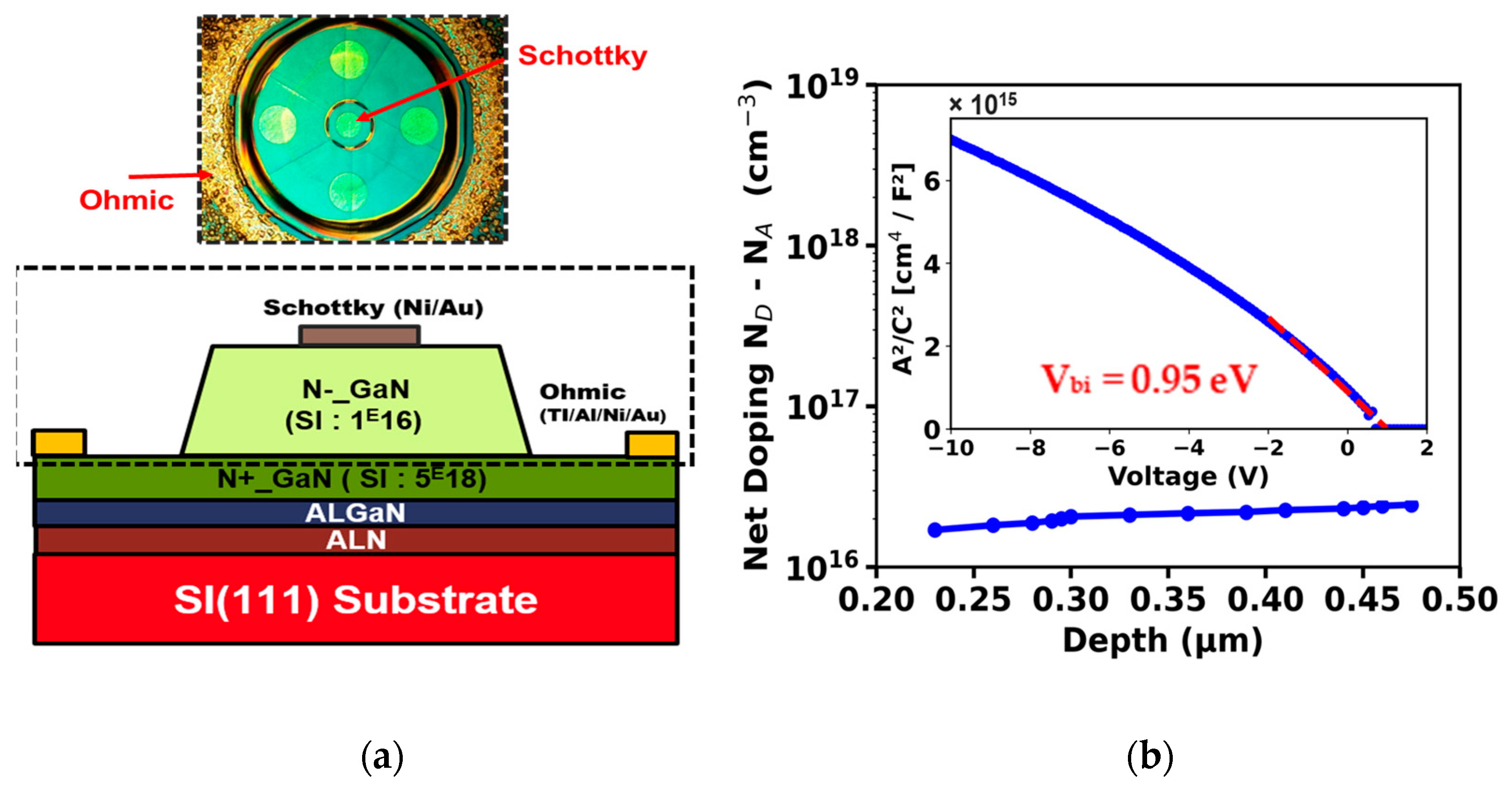
2. Materials and Methods
3. Results
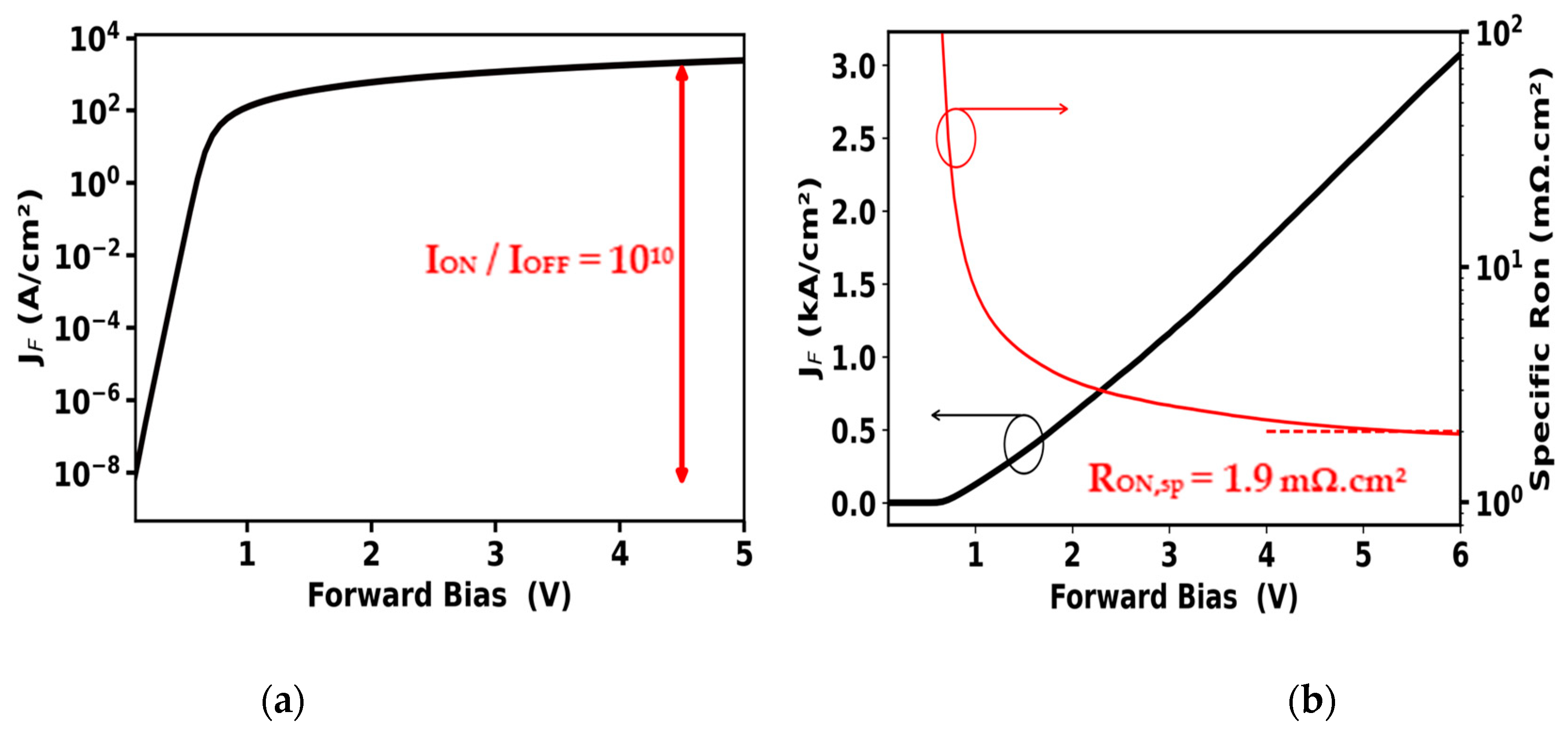
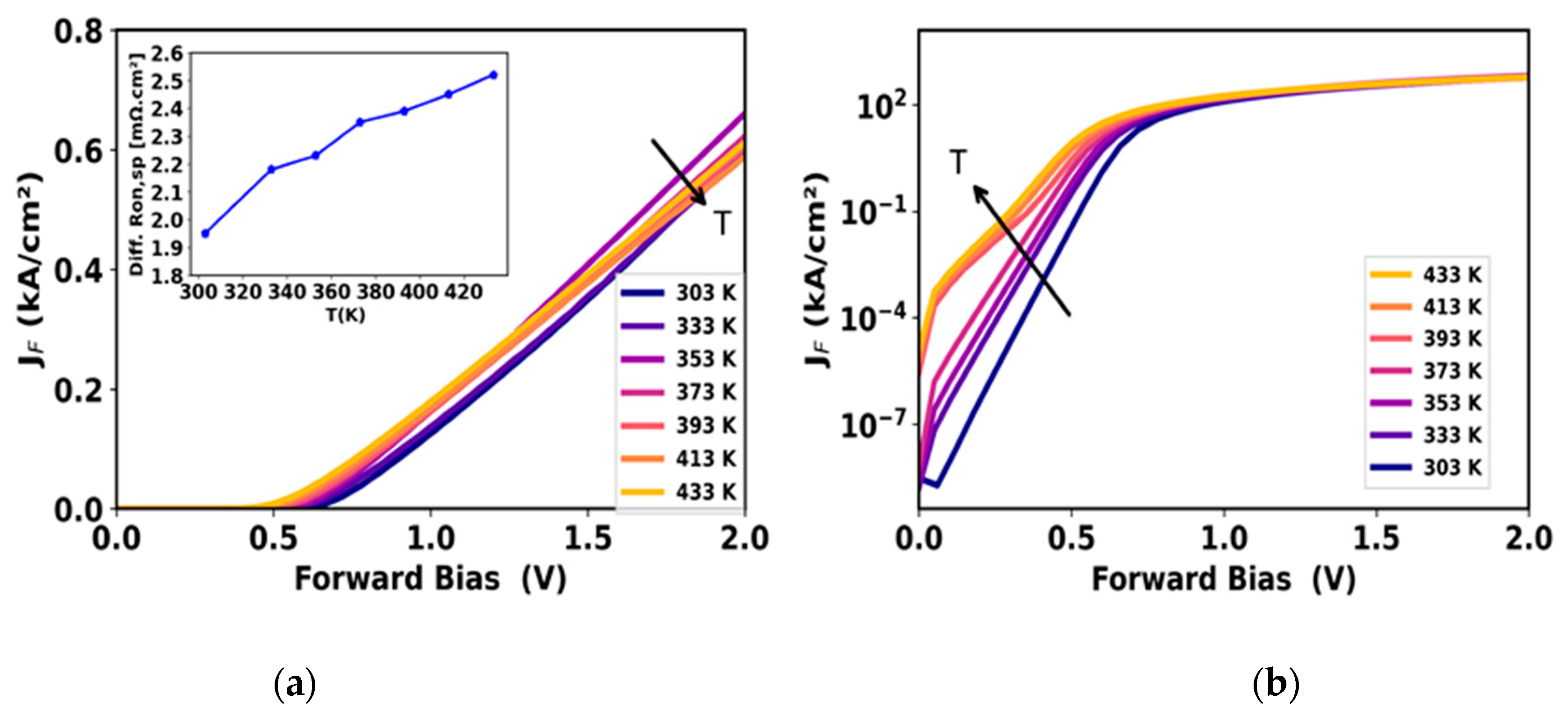
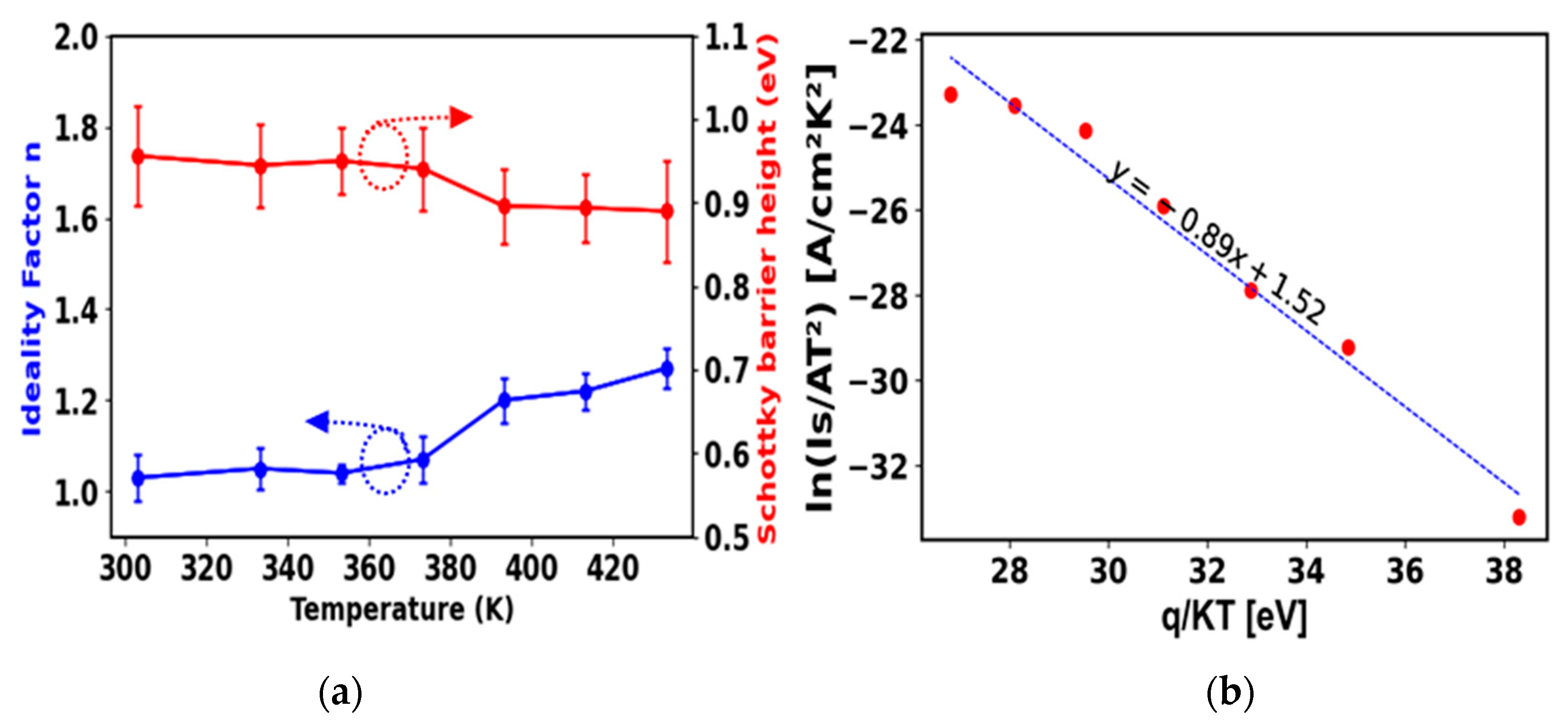
3.1. Forward Bias
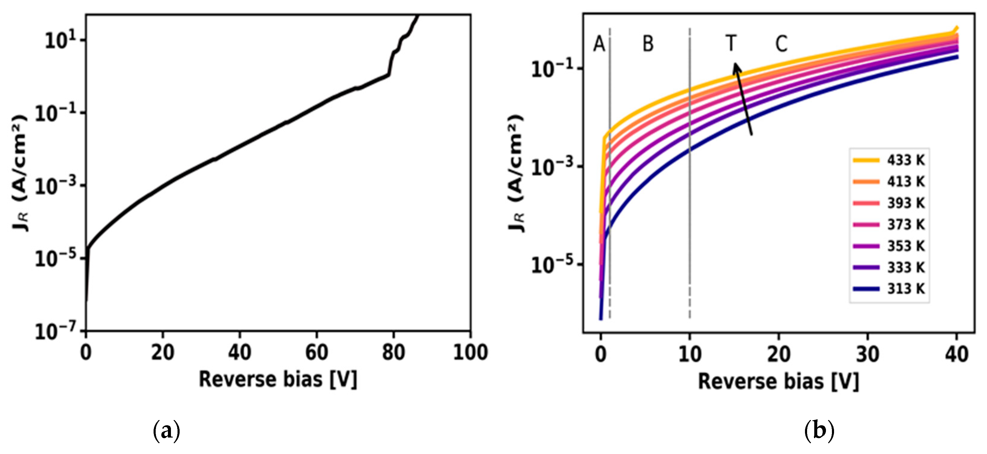
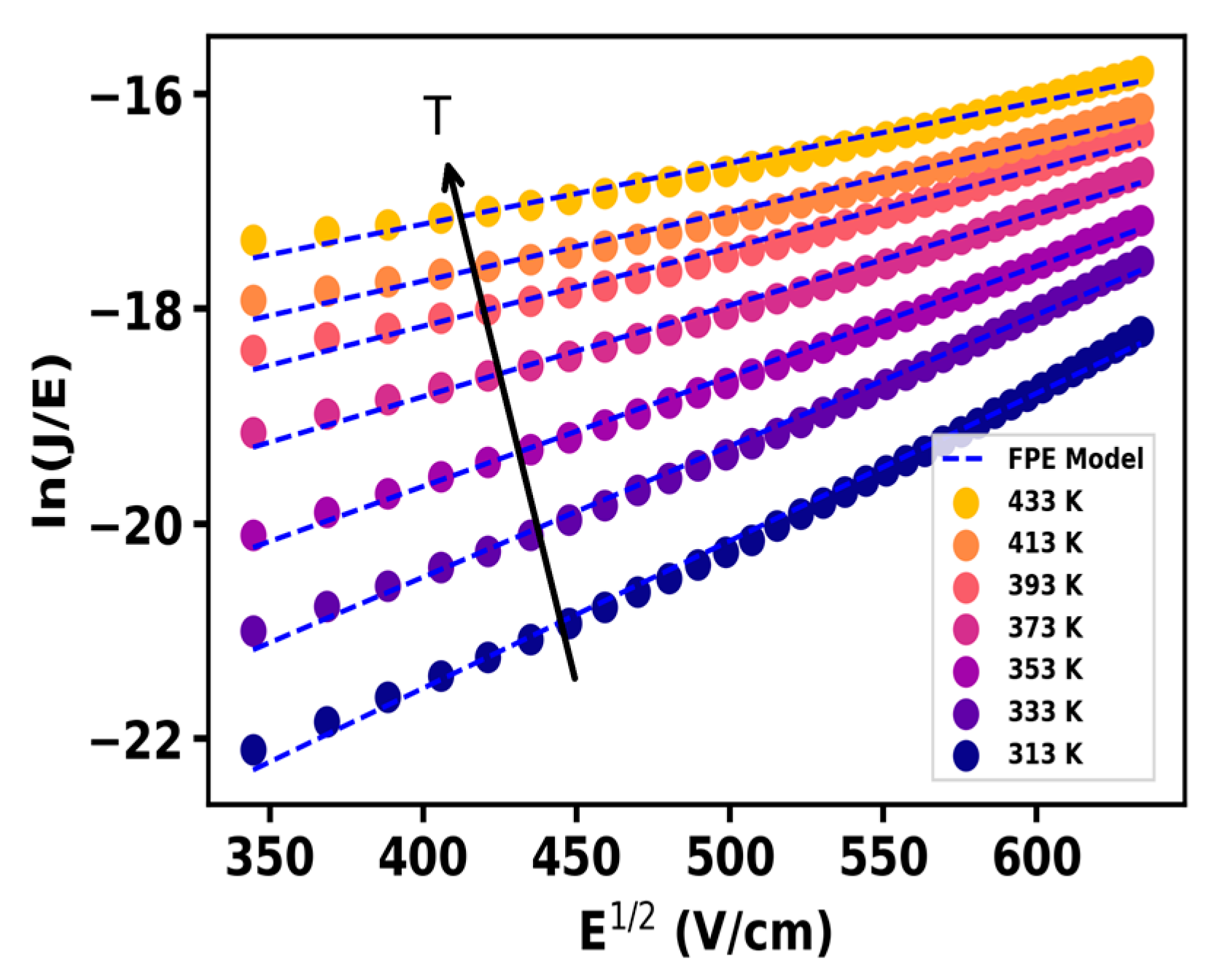
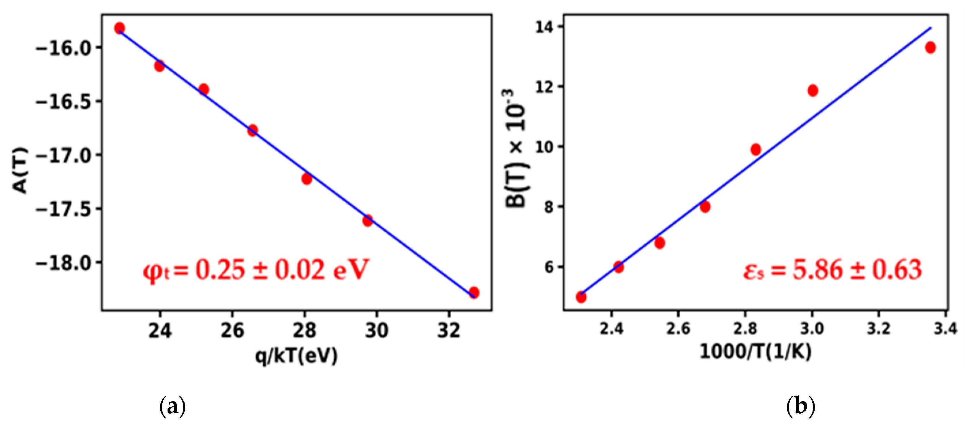
3.2. Reverse Bias
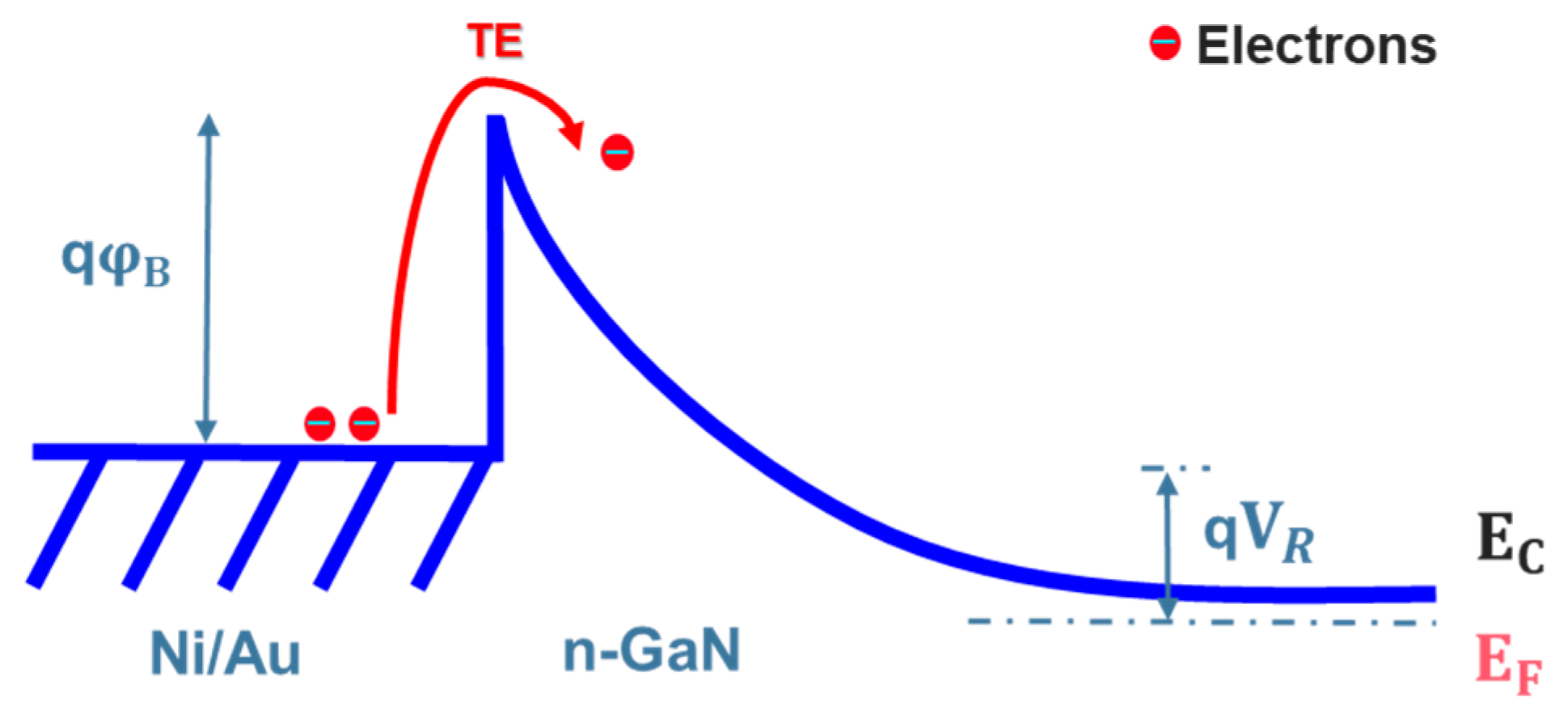
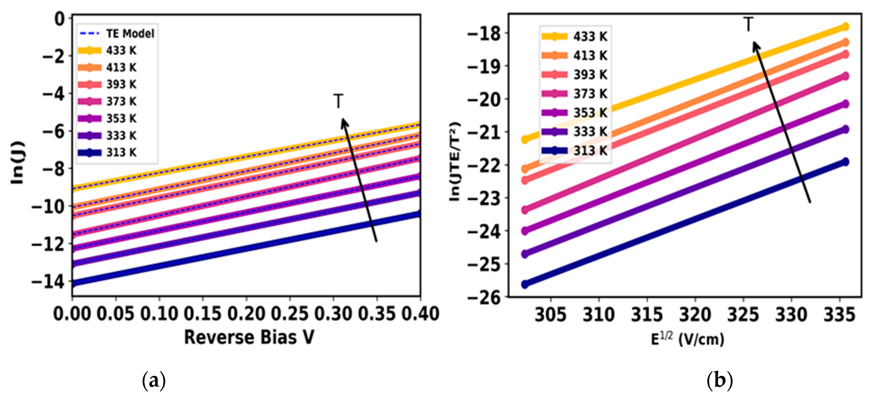
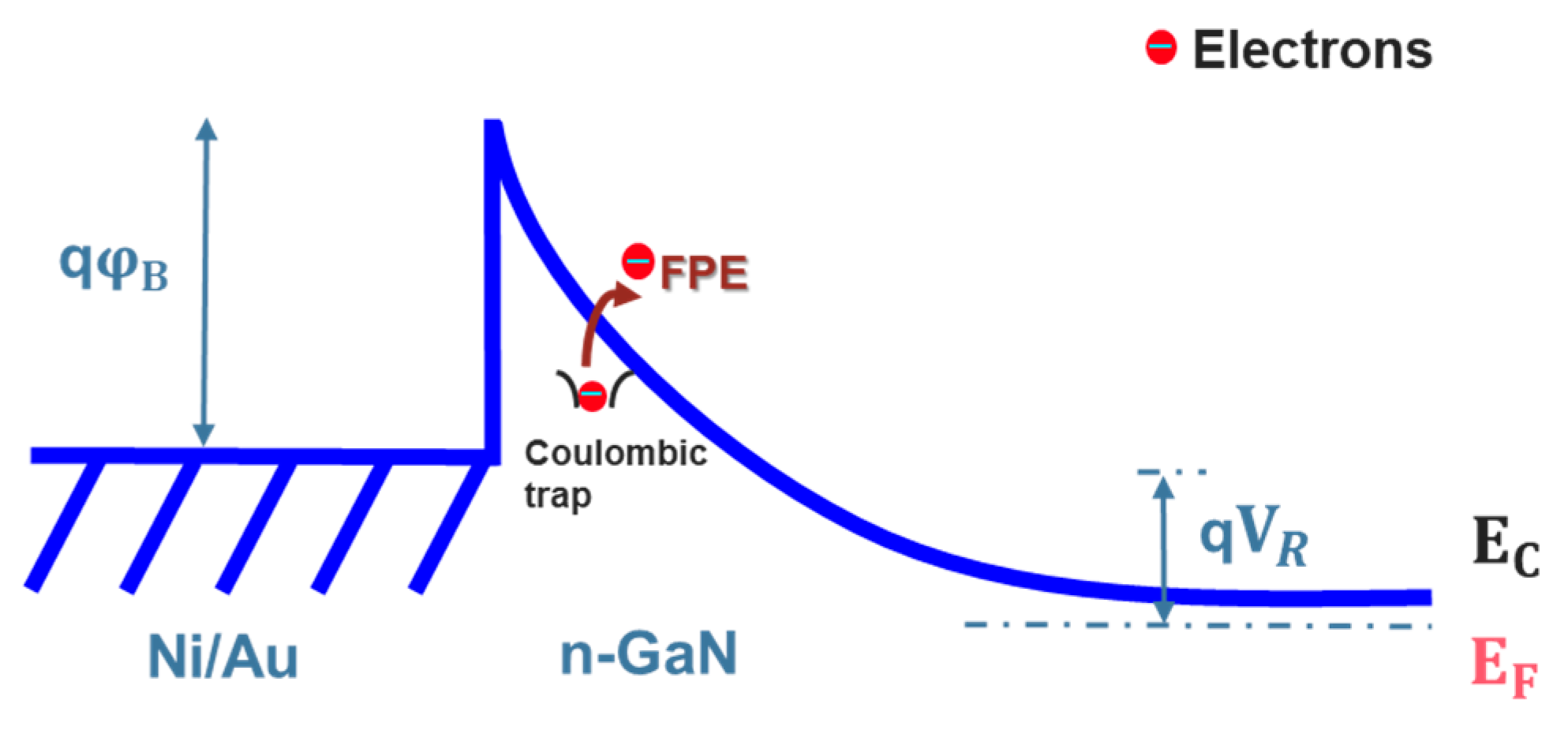
4. Discussion
5. Conclusions
Author Contributions
Funding
Data Availability Statement
Acknowledgments
Conflicts of Interest
References
- Dang, K.; Zhang, J.; Zhou, H.; Huang, S.; Zhang, T.; Bian, Z.; Zhang, Y.; Wang, X.; Zhao, S.; Wei, K.; et al. A 5.8-GHz High-Power and High-Efficiency Rectifier Circuit With Lateral GaN Schottky Diode for Wireless Power Transfer. IEEE Trans. Power Electron. 2020, 35, 2247–2252. [Google Scholar] [CrossRef]
- Chowdhury, S.; Stum, Z.; Li, Z.D.; Ueno, K.; Chow, T.P. Comparison of 600V Si, SiC and GaN Power Devices. Mater. Sci. Forum 2014, 778–780, 971–974. [Google Scholar]
- Langpoklakpam, C.; Liu, A.-C.; Hsiao, Y.-K.; Lin, C.-H.; Kuo, H.-C. Vertical GaN MOSFET Power Devices. Micromachines 2023, 14, 1937. [Google Scholar] [CrossRef] [PubMed]
- Zhang, Y.; Palacios, T. (Ultra)Wide-Bandgap Vertical Power FinFETs. IEEE Trans. Electron Devices 2020, 67, 3960–3971. [Google Scholar] [CrossRef]
- Baliga, B.J. Trends in power semiconductor devices. IEEE Trans. Electron Devices 1996, 43, 1717–1731. [Google Scholar] [CrossRef]
- Kachi, T. State-of-the-art GaN vertical power devices. In Proceedings of the 2015 IEEE International Electron Devices Meeting (IEDM), Washington, DC, USA, 7–9 December 2015; pp. 16.1.1-16.1.4. [Google Scholar]
- Hu, Z.; Nomoto, K.; Song, B.; Zhu, M.; Qi, M.; Pan, M.; Gao, X.; Protasenko, V.; Jena, D.; Xing, H.G. Near unity ideality factor and Shockley-Read-Hall lifetime in GaN-on-GaN p-n diodes with avalanche breakdown. Appl. Phys. Lett. 2015, 107, 243501. [Google Scholar] [CrossRef]
- Tanaka, N.; Hasegawa, K.; Yasunishi, K.; Murakami, N.; Oka, T. 50 A vertical GaN Schottky barrier diode on a free-standing GaN substrate with blocking voltage of 790 V. Appl. Phys. Express 2015, 8, 071001. [Google Scholar] [CrossRef]
- Guo, X.; Zhong, Y.; Zhou, Y.; Chen, X.; Yan, S.; Liu, J.; Sun, X.; Sun, Q.; Yang, H. 1200-V GaN-on-Si Quasi-Vertical p-n Diodes. IEEE Electron Device Lett. 2022, 43, 2057–2060. [Google Scholar] [CrossRef]
- Wei, Q.; Zhou, F.; Xu, W.; Ren, F.; Zhou, D.; Chen, D.; Zhang, R.; Zheng, Y.; Lu, H. Demonstration of Vertical GaN Schottky Barrier Diode With Robust Electrothermal Ruggedness and Fast Switching Capability by Eutectic Bonding and Laser Lift-Off Techniques. IEEE J. Electron Devices Soc. 2022, 10, 1003–1008. [Google Scholar] [CrossRef]
- Zou, X.; Zhang, X.; Lu, X.; Tang, C.W.; Lau, K.M. Breakdown Ruggedness of Quasi-Vertical GaN-Based p-i-n Diodes on Si Substrates. IEEE Electron Device Lett. 2016, 37, 1158–1161. [Google Scholar] [CrossRef]
- Zhang, Y.; Yuan, M.; Chowdhury, N.; Cheng, K.; Palacios, T. 720-V/0.35-m Ω·cm2 Fully Vertical GaN-on-Si Power Diodes by Selective Removal of Si Substrates and Buffer Layers. IEEE Electron Device Lett. 2018, 39, 715–718. [Google Scholar] [CrossRef]
- Tanaka, A.; Choi, W.; Chen, R.; Dayeh, S.A. Si Complies with GaN to Overcome Thermal Mismatches for the Heteroepitaxy of Thick GaN on Si. Adv. Mater. 2017, 29, 1702557. [Google Scholar] [CrossRef]
- Alquier, D.; Cayrel, F.; Menard, O.; Bazin, A.-E.; Yvon, A.; Collard, E. Recent Progresses in GaN Power Rectifier. Jpn. J. Appl. Phys. 2012, 51, 01AG08. [Google Scholar] [CrossRef]
- Kaltsounis, T.; Haas, H.; Lafossas, M.; Torrengo, S.; Maurya, V.; Buckley, J.; Mariolle, D.; Veillerot, M.; Gueugnot, A.; Mendizabal, L.; et al. Characterization of unintentional doping in localized epitaxial GaN layers on Si wafers by scanning spreading resistance microscopy. Microelectron. Eng. 2023, 273, 111964. [Google Scholar] [CrossRef]
- Zhang, Y.; Wong, H.Y.; Sun, M.; Joglekar, S.; Yu, L.; Braga, N.A.; Mickevicius, R.V.; Palacios, T. Design space and origin of off-state leakage in GaN vertical power diodes. In Proceedings of the 2015 IEEE International Electron Devices Meeting (IEDM), Washington, DC, USA, 7–9 December 2015; pp. 35.1.1-35.1.4. [Google Scholar] [CrossRef]
- Guo, X.; Zhong, Y.; Chen, X.; Zhou, Y.; Su, S.; Yan, S.; Liu, J.; Sun, X.; Sun, Q.; Yang, H. Reverse leakage and breakdown mechanisms of vertical GaN-on-Si Schottky barrier diodes with and without implanted termination. Appl. Phys. Lett. 2021, 118, 243501. [Google Scholar] [CrossRef]
- Maurya, V.; Buckley, J.; Alquier, D.; Irekti, M.-R.; Haas, H.; Charles, M.; Jaud, M.-A.; Sousa, V. Electrical Transport Characteristics of Vertical GaN Schottky-Barrier Diode in Reverse Bias and Its Numerical Simulation. Energies 2023, 16, 5447. [Google Scholar] [CrossRef]
- Sun, Y.; Kang, X.; Zheng, Y.; Lu, J.; Tian, X.; Wei, K.; Wu, H.; Wang, W.; Liu, X.; Zhang, G. Review of the Recent Progress on GaN-Based Vertical Power Schottky Barrier Diodes (SBDs). Electronics 2019, 8, 575. [Google Scholar] [CrossRef]
- Rhoderick, E.H.; Williams, R.H. Metal-Semiconductor Contacts; Clarendon Press: Oxford, UK, 1988; pp. 1–14. [Google Scholar]
- Chen, J.; Bian, Z.; Liu, Z.; Zhu, D.; Duan, X.; Wu, Y.; Jia, Y.; Ning, J.; Zhang, J.; Hao, Y. Effects of thermal annealing on the electrical and structural properties of Mo/Au schottky contacts on n-GaN. J. Alloys Compd. 2021, 853, 156978. [Google Scholar] [CrossRef]
- Phark, S.-H.; Kim, H.; Song, K.M.; Kang, P.G.; Shin, H.S.; Kim, D.-W. Current transport in Pt Schottky contacts to a-plane n-type GaN. J. Phys. Appl. Phys. 2010, 43, 165102. [Google Scholar] [CrossRef]
- Sang, L.; Ren, B.; Sumiya, M.; Liao, M.; Koide, Y.; Tanaka, A.; Cho, Y.; Harada, Y.; Nabatame, T.; Sekiguchi, T.; et al. Initial leakage current paths in the vertical-type GaN-on-GaN Schottky barrier diodes. Appl. Phys. Lett. 2017, 111, 122102. [Google Scholar] [CrossRef]
- Zhang, R.; Zhang, Y. Power device breakdown mechanism and characterization: Review and perspective. Jpn. J. Appl. Phys. 2023, 62, SC0806. [Google Scholar] [CrossRef]
- Simmons, J.G. Conduction in thin dielectric films. J. Phys. Appl. Phys. 1971, 4, 613. [Google Scholar] [CrossRef]
- Han, D.P.; Oh, C.H.; Kim, H.; Shim, J.I.; Kim, K.S.; Shin, D.S. Conduction Mechanisms of Leakage Currents in InGaN/GaN-Based Light-Emitting Diodes. IEEE Trans. Electron Devices 2015, 62, 587–592. [Google Scholar] [CrossRef]
- Peta, K.R.; Park, B.-G.; Lee, S.-T.; Kim, M.-D.; Oh, J.-E.; Kim, T.-G.; Reddy, V.R. Analysis of electrical properties and deep level defects in undoped GaN Schottky barrier diode. Thin Solid Films 2013, 534, 603–608. [Google Scholar] [CrossRef]
- Zhang, H.; Miller, E.J.; Yu, E.T. Analysis of leakage current mechanisms in Schottky contacts to GaN and Al0.25Ga0.75N∕GaN grown by molecular-beam epitaxy. J. Appl. Phys. 2006, 99, 023703. [Google Scholar] [CrossRef]
- Kuksenkov, D.V.; Temkin, H.; Osinsky, A.; Gaska, R.; Khan, M.A. Origin of conductivity and low-frequency noise in reverse-biased GaN p-n junction. Appl. Phys. Lett. 1998, 72, 1365–1367. [Google Scholar] [CrossRef]
- Chen, J.; Liu, Z.; Wang, H.; Song, X.; Bian, Z.; Duan, X.; Zhao, S.; Ning, J.; Zhang, J.; Hao, Y. Determination of the leakage current transport mechanisms in quasi-vertical GaN–on–Si Schottky barrier diodes (SBDs) at low and high reverse biases and varied temperatures. Appl. Phys. Express 2021, 14, 104002. [Google Scholar] [CrossRef]
- Look, D.C.; Reynolds, D.C.; Kim, W.; Aktas, Ö.; Botchkarev, A.; Salvador, A.; Morkoç, H. Deep-center hopping conduction in GaN. J. Appl. Phys. 1996, 80, 2960–2963. [Google Scholar] [CrossRef]
- Peta, K.R.; Kim, M.D. Leakage current transport mechanism under reverse bias in Au/Ni/GaN Schottky barrier diode. Superlattices Microstruct 2018, 113, 678–683. [Google Scholar] [CrossRef]
- Fu, K.; Fu, H.; Huang, X.; Yang, T.H.; Cheng, C.Y.; Peri, P.R.; Chen, H.; Montes, J.; Yang, C.; Zhou, J.; et al. Reverse Leakage Analysis for As-Grown and Regrown Vertical GaN-on-GaN Schottky Barrier Diodes. IEEE J. Electron Devices Soc. 2020, 8, 74–83. Available online: https://ieeexplore.ieee.org/abstract/document/8949530 (accessed on 1 May 2024). [CrossRef]
- Kwon, W.; Kawasaki, S.; Watanabe, H.; Tanaka, A.; Honda, Y.; Ikeda, H.; Iso, K.; Amano, H. Reverse Leakage Mechanism of Dislocation-Free GaN Vertical p-n Diodes. IEEE Electron Device Lett. 2023, 44, 1172–1175. [Google Scholar] [CrossRef]
- Rackauskas, B.; Dalcanale, S.; Uren, M.J.; Kachi, T.; Kuball, M. Leakage mechanisms in GaN-on-GaN vertical pn diodes. Appl. Phys. Lett. 2018, 112, 233501. [Google Scholar] [CrossRef]


| (3) | |||
| and ND − NA are extracted from CV measurements as mentioned above. | |||
| Mechanism | Expression | E Field Dependence | Temperature Dependence |
| Thermionic emission [20] | Yes | ||
| Frenkel–Poole [25] | |||
| Variable range hopping [26] | |||
| Phonon-assisted tunneling [27] | Insensitive | ||
Disclaimer/Publisher’s Note: The statements, opinions and data contained in all publications are solely those of the individual author(s) and contributor(s) and not of MDPI and/or the editor(s). MDPI and/or the editor(s) disclaim responsibility for any injury to people or property resulting from any ideas, methods, instructions or products referred to in the content. |
© 2024 by the authors. Licensee MDPI, Basel, Switzerland. This article is an open access article distributed under the terms and conditions of the Creative Commons Attribution (CC BY) license (https://creativecommons.org/licenses/by/4.0/).
Share and Cite
El Amrani, M.; Buckley, J.; Kaltsounis, T.; Arguello, D.P.; El Rammouz, H.; Alquier, D.; Charles, M. Study of Leakage Current Transport Mechanisms in Pseudo-Vertical GaN-on-Silicon Schottky Diode Grown by Localized Epitaxy. Crystals 2024, 14, 553. https://doi.org/10.3390/cryst14060553
El Amrani M, Buckley J, Kaltsounis T, Arguello DP, El Rammouz H, Alquier D, Charles M. Study of Leakage Current Transport Mechanisms in Pseudo-Vertical GaN-on-Silicon Schottky Diode Grown by Localized Epitaxy. Crystals. 2024; 14(6):553. https://doi.org/10.3390/cryst14060553
Chicago/Turabian StyleEl Amrani, Mohammed, Julien Buckley, Thomas Kaltsounis, David Plaza Arguello, Hala El Rammouz, Daniel Alquier, and Matthew Charles. 2024. "Study of Leakage Current Transport Mechanisms in Pseudo-Vertical GaN-on-Silicon Schottky Diode Grown by Localized Epitaxy" Crystals 14, no. 6: 553. https://doi.org/10.3390/cryst14060553
APA StyleEl Amrani, M., Buckley, J., Kaltsounis, T., Arguello, D. P., El Rammouz, H., Alquier, D., & Charles, M. (2024). Study of Leakage Current Transport Mechanisms in Pseudo-Vertical GaN-on-Silicon Schottky Diode Grown by Localized Epitaxy. Crystals, 14(6), 553. https://doi.org/10.3390/cryst14060553