Article

High-Performance Tandem White Micro-OLEDs for Virtual Reality and Mixed Reality Displays

College of Optics and Photonics, University of Central Florida, Orlando, FL 32816, USA
*
Author to whom correspondence should be addressed.
Crystals 2024, 14(4), 332; https://doi.org/10.3390/cryst14040332
Submission received: 11 March 2024 / Revised: 28 March 2024 / Accepted: 29 March 2024 / Published: 31 March 2024
(This article belongs to the Section Organic Crystalline Materials)

Abstract

:
To achieve wide-gamut and high-efficiency tandem white OLED (WOLED) microdisplays, we propose a new structure leveraging high-order antinodes and patterned microcavities. The color gamut coverages of 95% Rec. 2020 and 92% Rec. 2020 can be achieved in B/G/R tandem WOLED with a moderate microcavity and B/YG tandem WOLED with a strong microcavity, respectively. We have also boosted the optical efficiency by 62% for the tandem B/YG WOLED using the high-order antinodes at optimal conditions. Such a WOLED microdisplay helps reduce the power consumption of virtual reality (VR) and mixed reality (MR) displays while keeping a wide color gamut.

1. Introduction

Organic light-emitting diodes (OLED) have been widely used in flat panel displays ranging from smartphones to televisions [1,2]. With the rapid development of augmented reality (AR) and virtual reality (VR), conventional active-matrix OLED on glass substrate cannot meet the high-resolution density requirement because multiple thin film transistors (TFTs) are employed in each pixel. To greatly increase resolution density, OLED-on-silicon (also called Micro-OLED) has been developed. Compared to liquid crystal displays (LCDs) [3,4,5], OLED-on-silicon exhibits a higher resolution density, higher native contrast ratio, smaller form factor and faster response time. The US-based corporation eMagin employed red, green, and blue (RGB) OLEDs to generate full color [6]. However, the fabrication of small pixel-sized (<10 µm) RGB OLEDs is rather challenging because of the shadow effect of fine metal masks [7], so some other companies such as Sony [8] and Kopin focus on white OLED (WOLED) with color filters. But the efficiency and color gamut are the bottlenecks due to wide emission spectra of WOLEDs and the absorption and crosstalk of the color filters.
The simplest architecture of WOLEDs is single stack. However, the efficiency and lifetime of the single-stack WOLED need to be improved because only about 25% of the white light transmits through the absorptive color filters. Tandem WOLEDs [9,10,11,12] have been developed to improve the current efficiency. Several emission layers (EMLs) are connected by charge generation layers (CGLs), which usually consist of an n-p semiconductor heterojunction layer [13]. Spatially separated recombination zones not only increase the current efficiency but also enable the EMLs to be located at respectively optimal positions according to the microcavity design. For example, LG Display reported a 3-stack WOLED in 2024 and Kopin demonstrated a 2-stack WOLED with an average current efficiency of 12 cd/A [14]. More (e.g., 4 or 5) stacks are possible, as demonstrated by OLEDWorks [15], but the driving voltage is inevitably increased. Considering the balance between driving voltage and current efficiency, in this paper, we adopt a 2-stack tandem WOLED structure. Despite a higher current efficiency enabled by the tandem structures, the brightness and lifetime of the WOLEDs are still inadequate for waveguide-based AR applications [16]. In this aspect, III-nitride micro-LED [17] using inorganic materials exhibits enormous potential to achieve ultrahigh brightness while maintaining a long lifetime. However, some issues, such as cost-effective manufacturing and decreased light efficiency due to sidewall defects, remain to be overcome before its widespread adoption for AR glasses can be realized. For VR applications, the required brightness for the light engine is around 10,000 nits, which the tandem OLEDoS can achieve relatively easily. For those reasons, we focus on investigating 2-stack tandem white micro-OLEDs for VR applications. With the integration of several cameras in VR headsets, mixed reality (MR) enabled by the video see-through function can allow users to interact with the ambient world. Besides a high efficiency and low power consumption, a wide color gamut is crucial for high-performance VR/MR headsets. However, the color gamut of WOLEDs is usually smaller than 100% DCI-P3 because of their wide emission spectra and the crosstalk of color filters. For example, Sony reported a micro-OLED with a color gamut of 108% sRGB [8], and BOE developed a micro-OLED with a color gamut of 90% DCI-P3 in Display Week 2023. More recently, Apple Vision Pro exhibits a color gamut of 92% DCI-P3.
To widen the color gamut while keeping a high efficiency, we propose a new structure leveraging high-order antinodes and patterned microcavities. To analyze and optimize the performance of the whole system, we first simulate the performance of WOLED and pancake VR, and then introduce five independent variables. We also investigate two kinds of 2-stack tandem WOLEDs: B/YG and B/G/R. The former refers to a blue emission layer (EML) and a yellow green (YG) EML; the latter represents a blue EML, a green EML, and a red EML. Our simulation results prove that the proposed structure helps B/YG and B/G/R WOLEDs achieve a wider color gamut and higher efficiency. The color gamut covers 95% Rec. 2020 and 92% Rec. 2020 for the B/G/R WOLED with a moderate microcavity and B/YG WOLED with a strong microcavity, respectively. To the best of our knowledge, 95% Rec. 2020 is the largest reported color gamut for the WOLEDs with color filters. For the B/YG WOLED, we can boost its efficiency by 62% using the high-order antinodes at optimal conditions. We foresee such an improved WOLED structure will contribute to a more vivid and efficient VR/MR display.

2. System Modelling

The performance of a WOLED microdisplay is determined by several factors, such as thin metal film, capping layer, number, and the position of the EMLs and color filters. For this reason, the WOLED structure should be well optimized. Meanwhile, the display performance of the VR system is jointly determined by the microdisplay light engine and the imaging optics. Thus, the WOLED microdisplay and pancake optical system will be modelled in sequence, forming the basis for the optimization processes. All calculations regarding the entire system are implemented using home-made MATLAB codes.

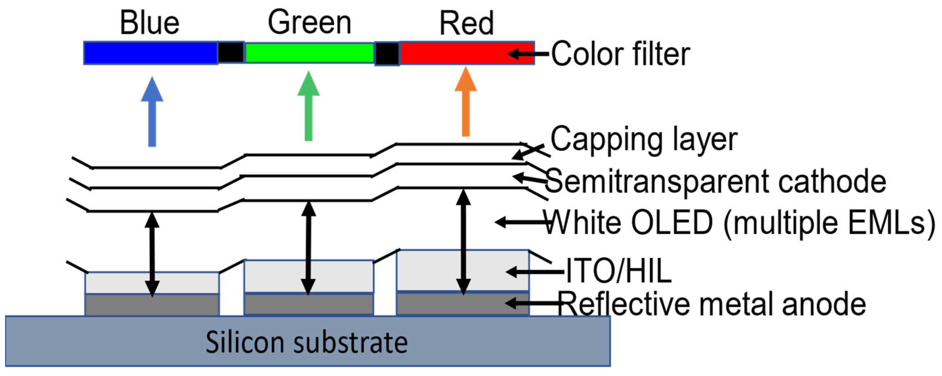
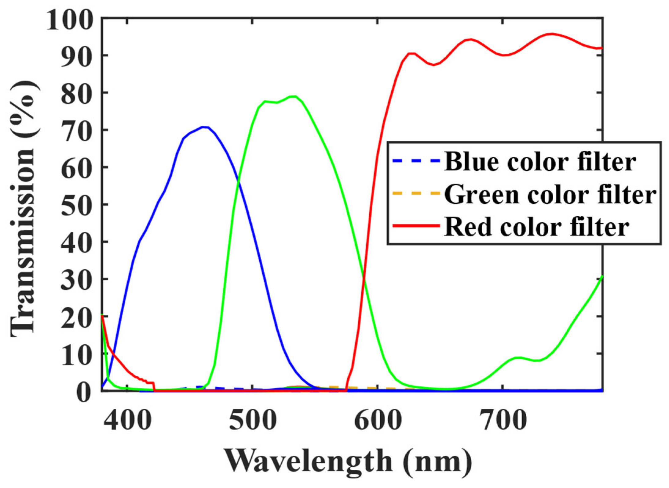
2.1. Tandem WOLED Microdisplay

The proposed WOLED comprises several tandem EMLs. The simplest tandem structure consists of one fluorescent blue EML and one phosphorescent yellow EML. Different from conventional OLED TVs, the driving voltage of the OLED microdisplay is limited by the complementary metal-oxide-semiconductor (CMOS) circuits. Therefore, a low operating voltage is critical for WOLED microdisplays. To improve the color gamut and transmittance through color filters, we also leverage microcavities by introducing different optical cavity lengths for the red, green, and blue subpixels [18]. More specifically, indium tin oxide (ITO) or hole injection layer (HIL) can be patterned below the common EMLs, as shown in Figure 1. Compared to conventional microcavity tandem white micro-OLEDs where all the EMLs are placed in the respective antinode positions, the Fabry–Perot microcavity with patterned layers helps narrow the emission spectra before the light transmits through the color filters. More specifically, a certain EML is placed in the antinode position to create constructive interference while another EML is placed in the node position to produce destructive interference.
To quantify the WOLED performance in a VR system, total light efficiency (TLE), color gamut coverage (CGC), and color nonuniformity are considered. TLE is the product of following three parameters: external quantum efficiency (EQE), optical transmission efficiency of color filters (ηCF), and optical system efficiency (ηOSE), as Equation (1) indicates:
T L E = E Q E η C F η O S E = ( η O C E I Q E ) η C F η O S E ,
More explicitly, EQE is the product of outcoupling efficiency (ηOSE) and internal quantum efficiency (IQE). The outcoupling efficiency can be calculated by the rigorous dipole model. The transmission efficiency of color filters can be calculated using Equation (2):
η C F = K ( θ , λ ) T C F ( λ ) d θ d λ K ( θ , λ ) d θ d λ ,
where K (θ, λ) is the power dissipation density corresponding to different emission angles and wavelength, and TCF (λ) is the transmission spectra of color filters, as shown in Figure 2. A higher transmission efficiency will contribute to a higher TLE. Equation (3) shows how to calculate the optical system efficiency (ηOSE):
η O S E = ( K ( θ , λ ) T C F ( λ ) d λ ) sin ( θ ) η c ( θ , p ) d θ d p ( K ( θ , λ ) T C F ( λ ) d λ ) sin ( θ ) d θ d p
where ηc (θ, p) is the collection efficiency depending on the emission angle and the location of the point source, which is calculated as the ratio of power collected by the eye pupil to the power emitted from the point source. According to Equation (3), ηOSE is impacted by the emission cone of the display panel and the collection cone. The emission cone is usually much larger than the collection cone, thus leading to low optical system efficiency. Thus, a moderate or strong microcavity helps narrow down the angular distributions of the emitting pixels and thereby increase the optical efficiency. To quantify the color performance in a VR system, the position-dependent spectrum is defined in Equation (4):
S λ , p = K ( θ , λ ) · T C F ( λ ) · s i n ( θ ) · η c ( θ , p ) d θ
Then, the CGC of the central pixel (p = 0) is defined in Equation (5):
C G C = A d i s p l a y A s t a n d a r d A s t a n d a r d
where Adisplay is the triangular area of the display whose three vertices are color coordinates calculated from Sred (λ, 0), Sgreen (λ, 0), and Sblue (λ, 0), respectively, and Astandard is the triangular area of the reference standard (DCI-P3 or Rec. 2020). Stronger microcavities help narrow the emission spectra, leading to a larger CGC. But the TLE may decrease and the color nonuniformity may increase. Lastly, the color nonuniformity is defined as the color difference between the central pixel and the neighboring pixels. Considering color mixing, the maximum color nonuniformity of the first 18 colors in Macbeth Color Checker is defined as the color nonuniformity in a VR system. For a tandem WOLED, TLE, and CGC, color nonuniformity can be obtained by incoherently superimposing the power dissipation density K of randomly oriented dipoles in different EMLs.

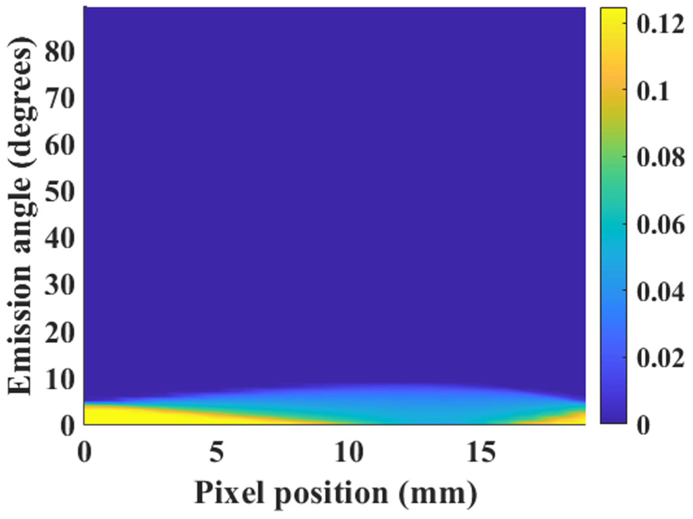
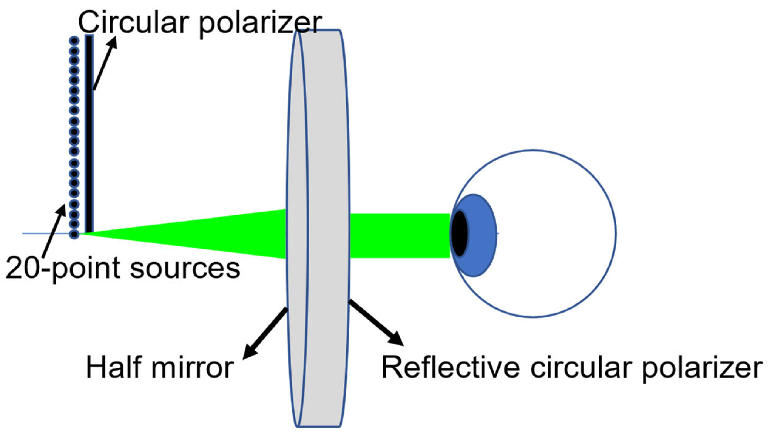
2.2. Pancake Optical System

The pancake lens has become the mainstream of VR/MR headsets because of its compact form factor. Here, we build a raytracing model in the LightTools software, as shown in Figure 3. In this model, the distance from the display to the lens is 16.4 mm, the diameter of the lens is 41.2 mm, and the eye relief is 13.3 mm. We model the display panel using 20-point sources with 1-mm spacing, which can achieve a ~100° horizontal field of view with the magnification of the pancake lens. The diameter of the eye pupil is 4 mm. The reflective circular polarizer can be made of a broadband quarter-wave plate and a reflective linear polarizer, or by simply using a cholesteric liquid crystal film. In our model, a broadband quarter-wave plate and a reflective polarizer based on multilayer thin films are employed to function as a reflective circular polarizer. Figure 4 depicts the collection efficiency depending on the emission angle and the location of the point source. The maximum collection efficiency of ~12.5% is attributed to the 50% absorption loss of a circular polarizer placed in front of the point sources and the 75% loss from traversing through the half mirror twice. As a comparison, if we adopt a wire grid polarizer to act as a reflective linear polarizer, the maximum collection efficiency is reduced to ~10% due to its intrinsic absorption. On the other hand, the collection cone for almost all pixels falls within ~5°, arising from a telecentric design of the pancake lens and a small eye pupil.

3. Analysis and Optimization

Based on Figure 1, the layer from the bottom to the top can be listed as follows: CMOS/anode/ITO/HIL/HTL/B-EML/CGL/YG-EML (or other EMLs) /ETL/Cathode (thin Mg:Ag alloy)/Capping (CMOS stands for complementary metal-oxide-semiconductor; HTL refers to hole transportation layer; ETL represents electron transportation layer). We consider the wavelength-dependent refractive index for anode, ITO, and cathode and assume the same refractive index of 1.8 for all remaining organic layers. Different EMLs are connected in series with a charge generation layer (CGL). The thickness of the anode layer is 100 nm to provide a high reflection. All the EML thicknesses are 10 nm, and the thickness of the ETL is 30 nm. If HIL is patterned to introduce different optical cavity lengths, the ITO thickness is fixed at 10 nm. If ITO is patterned, the HIL thickness is fixed at 20 nm. To perform system-level analysis and optimization, we introduce five independent variables, which can be denoted by D = [d1, d2, d3, d4, d5]. More specifically, d1, d2, and d3 are the HIL or ITO thicknesses corresponding to blue, green, and red subpixels, respectively, d4 is the cathode thickness, and d5 is the capping thickness. The former three variables [d1, d2, d3] mainly modulate the radiated intensity of multiple emissive layers; the latter two variables [d4, d5] mainly impact the resonance strength and the efficiency. For [d4, d5], we set d4  [10 nm, 25 nm] and d5  [0 nm, 80 nm], respectively. Lastly, our optimization target is to find the maximum TLE while keeping a color gamut coverage of no less than 99% DCI-P3 and the color nonuniformity Δ u v ≤ 0.02. Considering three subpixels, the TLE is calculated as the averaged efficiency of three subpixels. We also investigate how wide the color gamut can be since a larger color coverage leads to a better color saturation and viewer satisfaction [19].

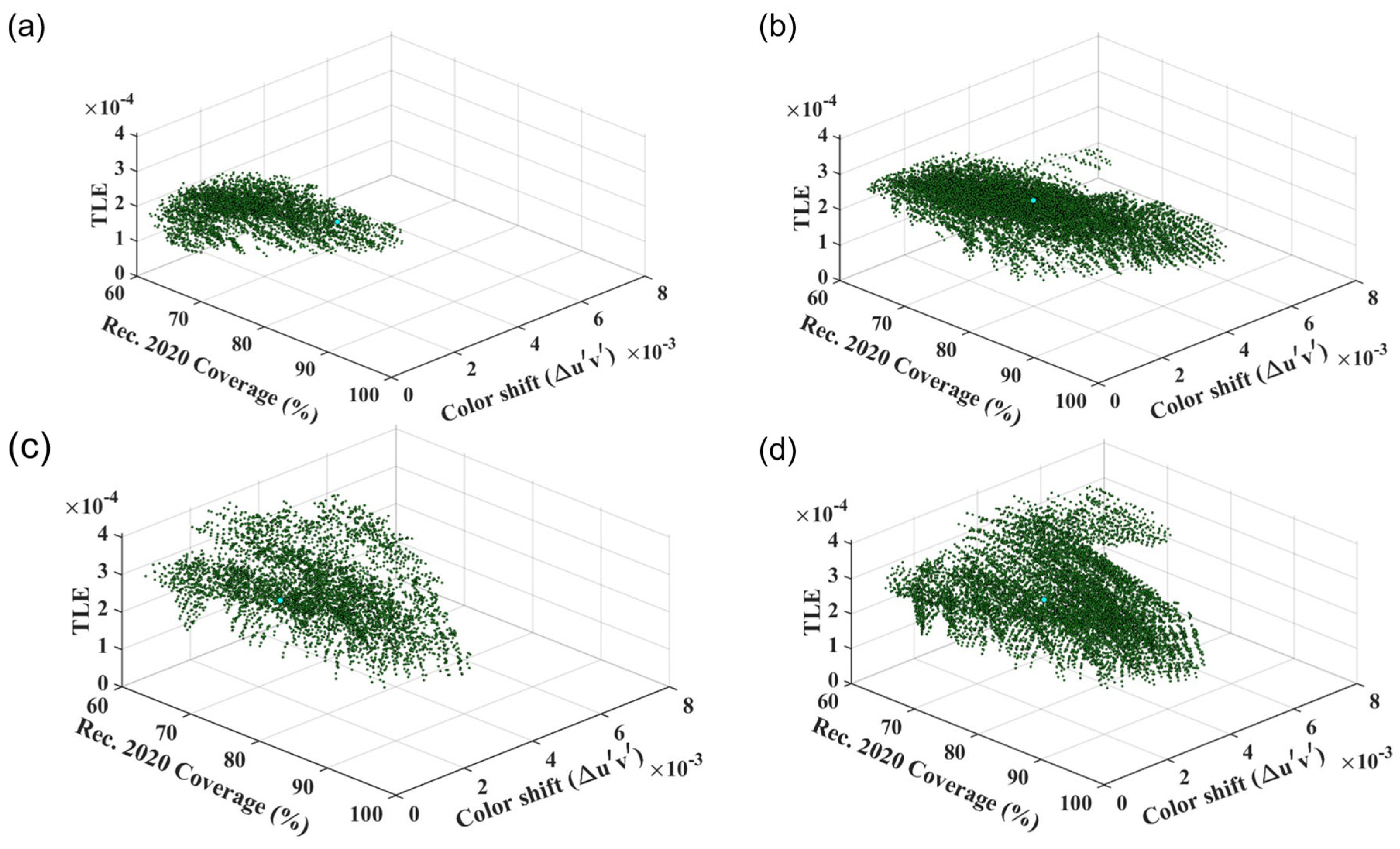
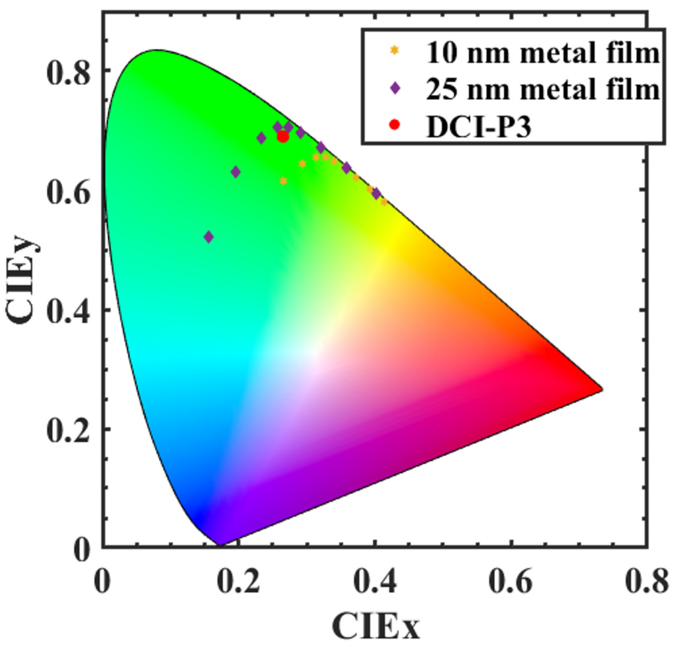
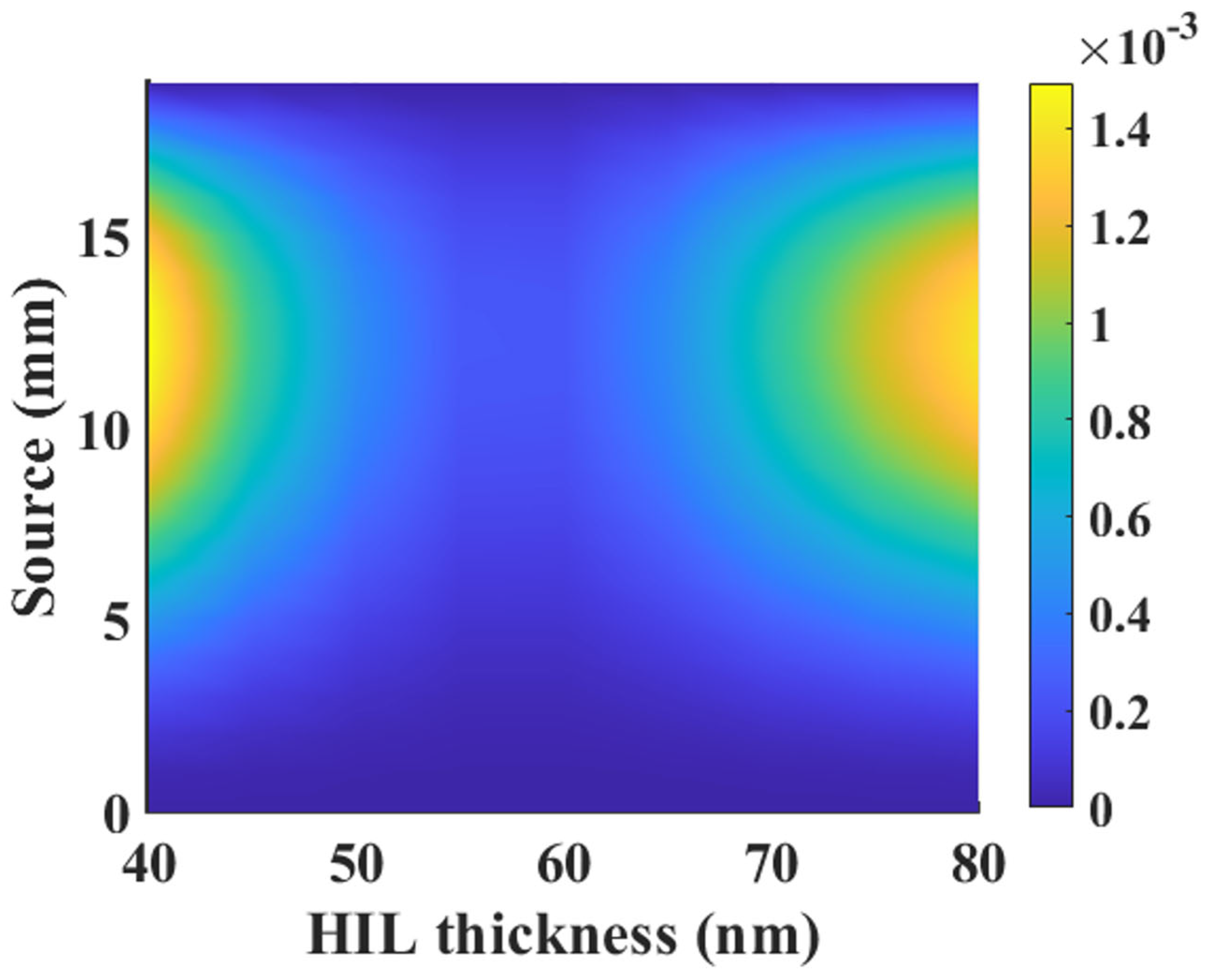
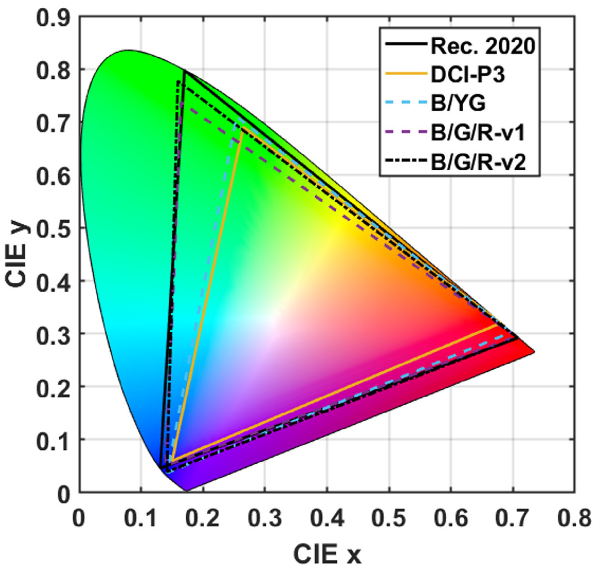
3.1. B/YG Tandem WOLED

In this section, we study the simplest tandem structure: B/YG WOLED. It usually exhibits a lower driving voltage than that with more emissive layers. In the blue subpixel, the microcavity should be designed to obtain constructive interference for blue light and destructive interference for yellow–green light. To achieve a minimum thickness, we can locate the blue emitter around the first antinode of the reflective metal electrode and the yellow–green emitter around the first node of the reflective metal electrode. Therefore, the spacing between the two EMLs and the CGL thickness can be calculated, which is approximately 90 nm and 80 nm, respectively. Due to the CGL thickness, it is not possible to achieve the first antinode corresponding to the yellow–green emitter, and thus the second antinode can be employed. Via physical analysis, we choose d1 ∈ [5 nm, 35 nm], d2 ∈ [40 nm, 80 nm], and d3 ∈ [85 nm, 120 nm] as boundary constraints. In the following, we use a green subpixel as a preliminary demonstration because it greatly determines how wide the color gamut can be.
Figure 5 shows the spectra of the green subpixel corresponding to different angles, as indicated by solid lines. As a reference, the emission spectra of the blue (BPPyA) and yellow–green (Ir ( t p t p y ) 2 acac) emitters are also included [18] using dashed lines. If d2 (HIL) = 60 nm, d4 = 25 nm, and d5 = 60 nm, we can obtain the spectrum with a central wavelength of 538 nm and the full width at half maximum FWHM = 32 nm. Such a narrow FWHM arises from the strong microcavity effect. If ITO is selected to control the cavity length corresponding to the green subpixel, we can calculate d2 (ITO) = 50 nm to achieve a similar result to Figure 5. To investigate how d2 and d4 impact the transmitted spectra, we calculate the spectra and color coordinates corresponding to different values for d2 and d4. As Figure 6 depicts, a thicker Mg:Ag film helps achieve DCI-P3′s green primary given a certain d2.
Besides color coordinates, position-dependent color shift corresponding to different d2 is also simulated, as shown in Figure 7. For the source (pixel) positions ranging from 10 mm to 15 mm, the maximum color shift occurs. This is because the maximum collection efficiency corresponding to those pixel positions occurs at larger emission angles (~10°), as shown in Figure 4, leading to a larger color shift.
According to this demonstration, it is feasible to eliminate the green color filter because the blue light can be suppressed almost completely by the destructive interference under certain conditions, as verified by Figure 5. The same conclusion also applies to the blue subpixel because of the destructive interference of yellow–green light. Although color filters help increase ambient contrast ratio, this advantage may disappear because we can laminate another quarter-wave plate onto the circular polarizer to eliminate the reflected light from the half mirror. Compared to the blue and green subpixels, it is more challenging to eliminate the red color filter. In a red subpixel, we would like to locate the yellow–green emitter around the second antinode for a resonance wavelength of ~630 nm. Unfortunately, the blue emitter is simultaneously located closer to the second antinode for a resonance wavelength of ~460 nm. For this reason, dual peaks emerge in the red subpixel. To improve optical efficiencies of the blue and green subpixels and achieve a decent color gamut, we can just pattern the red color filters.
As mentioned above, we can achieve DCI-P3′s green primary with the low-order antinodes with a strong microcavity; however, the efficiency is inevitably reduced due to the higher absorption of the metal cathode. According to the principles of interference, a longer cavity length contributes to generating the spectrum with a narrower FWHM. Therefore, we propose a B/YG WOLED with high-order antinodes to improve the color gamut and efficiency. We repeat the same optimization process as the low-order antinodes except that d1 ∈ [110 nm, 150 nm], d2 ∈ [160 nm, 200 nm], d3 ∈ [230 nm, 280 nm], and the CGL thickness is 110 nm. Compared to the low-order antinodes, we locate the blue emitter around the second antinode of the reflective metal electrode and the yellow–green emitter around the second node of the reflective metal electrode. The optimized result shows that the maximum color gamut can increase from 80% to 92% Rec. 2020. Also, the layer thicknesses for optimal solutions corresponding to the low-order antinodes and high-order antinodes are Dl = [25 nm, 55 nm, 115 nm, 20 nm, 80 nm] and Dh = [120 nm, 180 nm, 255 nm, 15 nm, 80 nm], respectively. The corresponding optimal TLE is 1.39 × 10 4 and 2.26 × 10 4 , respectively. The 1.6x TLE mainly arises from the reduced cathode thickness (d4) required to achieve a color gamut of no less than 99% DCI-P3. Note that a higher-order antinode helps to further widen the color gamut, but the efficiency may be reduced, and the conductivity could be an issue for organic layers, which can be mitigated by organic materials with high carrier mobilities [20].

3.2. B/G/R Tandem WOLED

In this section, we investigate another tandem structure: B/G/R WOLED. We input the emitted spectra from three EMLs, and then repeat the same optimization procedures as the B/YG WOLED. Figure 8 compares the color gamut coverage between the B/YG WOLED and the B/G/R WOLED with the low-order antinodes. When Dl = [20 nm, 55 nm, 120 nm, 25 nm, 0 nm], 100% DCI-P3 or 80% Rec. 2020 can be achieved via B/YG. To achieve a much wider color gamut, deep green with a high CIE y value is highly desired. With a green EML and a designed cavity, B/G/R-v2 and B/G/R-v1 can achieve a color gamut of 95% and 90% Rec. 2020, respectively, when Dl = [10 nm, 50 nm, 110 nm, 25 nm, 0 nm] and Dl = [5 nm, 45 nm, 120 nm, 10 nm, 80 nm], respectively. To achieve an ultrawide color gamut while keeping a high efficiency, we propose a B/G/R WOLED with high-order antinodes, just like B/YG WOLED. For example, when Dh = [110 nm, 165 nm, 255 nm, 15 nm, 0 nm], a color gamut with 95% Rec. 2020 can be achieved with a 15-nm cathode. This structure also enables a color gamut of 93% Rec. 2020 with a 10-nm cathode when Dh = [110 nm, 165 nm, 265 nm, 10 nm, 80 nm].
For B/G/R WOLEDs, the layer thicknesses for optimal solutions corresponding to the low-order antinodes and the high-order antinodes are Dl = [5 nm, 55 nm, 100 nm, 10 nm, 80 nm] and Dh = [115 nm, 175 nm, 245 nm, 10 nm, 80 nm], respectively. The corresponding optimal TLE is 3.64 × 10 4 and 3.58 × 10 4 , respectively. In comparison with B/YG WOLED with the low-order antinodes, ~160% efficiency improvement is mainly attributed to the 10-nm cathode. All optimal solutions are marked in Figure 9.

4. Conclusions and Future Perspectives

We have modelled the performance of WOLED in pancake VR headsets, forming the basis for systematical analysis and optimization. For both B/YG and B/G/R WOLED, we first analyzed the boundary constraints for [d1, d2, d3] to speed up the simulation process, and then optimized their performance. Our results indicated that it is possible to eliminate the blue and green color filters to improve the optical efficiencies of B/YG WOLED. More importantly, we proposed a new structure by combining the high-order antinodes with the patterned microcavities. Our simulation results also indicated that our proposed structure can improve the efficiency of B/YG tandem WOLED from 1.39 × 10 4 (corresponding to low-order antinodes) to 2.26 × 10 4 (corresponding to high-order antinodes) at optimal conditions. It also enabled a color gamut coverage of 92% Rec. 2020 in B/YG WOLED with a strong microcavity. For B/G/R tandem WOLED, a color gamut of 95% Rec. 2020 can be achieved with a moderate microcavity when Dh = [110 nm, 165 nm, 255 nm, 15 nm, 0 nm] (the cathode thickness is 15 nm).
Overall, the proposed methods help achieve tandem white micro-OLED with wide color gamut and high efficiency. These are important to VR/MR headsets. In the near-term, tandem white micro-OLED integrated with patterned microcavities, microlens arrays, and optimized color filters is expected to dominate high-end VR/MR markets because of its high-resolution density, high efficiency, and wide color gamut. In the long- term, however, tandem RGB micro-OLEDs without color filters could be a strong contender if the cost-effective manufacturing technology can be realized.

Author Contributions

Methodology, Z.Y. and E.-L.H.; simulations, Z.Y.; writing—original draft preparation, Z.Y.; writing—review and editing, S.-T.W.; supervision, S.-T.W. All authors have read and agreed to the published version of the manuscript.

Funding

The UCF group is indebted to Nichia for the partial financial support.

Data Availability Statement

The data presented in this study are available from the authors upon reasonable request.

Conflicts of Interest

The authors declare no conflicts of interest.

References

  1. Tang, C.W.; VanSlyke, S.A. Organic Electroluminescent Diodes. Appl. Phys. Lett. 1987, 51, 913–915. [Google Scholar] [CrossRef]
  2. Baldo, M.A.; Lamansky, S.; Burrows, P.E.; Thompson, M.E.; Forrest, S.R. Very High-Efficiency Green Organic Light-Emitting Devices Based on Electrophosphorescence. Appl. Phys. Lett. 1999, 75, 4–6. [Google Scholar] [CrossRef]
  3. Hsiang, E.-L.; Yang, Z.; Yang, Q.; Lai, P.-C.; Lin, C.-L.; Wu, S.-T. AR/VR Light Engines: Perspectives and Challenges. Adv. Opt. Photonics 2022, 14, 783–861. [Google Scholar] [CrossRef]
  4. Yang, Z.; Hsiang, E.L.; Qian, Y.; Wu, S.T. Performance Comparison between Mini-LED Backlit LCD and OLED Display for 15.6-Inch Notebook Computers. Appl. Sci. 2022, 12, 1239. [Google Scholar] [CrossRef]
  5. Yang, Z.; Qian, Y.; Zou, J.; Lee, C.-L.; Lin, C.-L.; Wu, S.-T. Reducing the Power Consumption of VR Displays with a Field Sequential Color LCD. Appl. Sci. 2023, 13, 2635. [Google Scholar] [CrossRef]
  6. Ghosh, A.; Donoghue, E.P.; Khayrullin, I.; Ali, T.; Wacyk, L.; Tice, K.; Vazan, F.; Prache, O.; Wang, Q.; Sziklas, L.; et al. 18-1: Invited Paper: Ultra-High-Brightness 2K x 2K Full-Color OLED Microdisplay Using Direct Patterning of OLED Emitters. SID Symp. Dig. Tech. Pap. 2017, 48, 226–229. [Google Scholar] [CrossRef]
  7. Kim, C.; Kim, K.; Kwon, O.; Jung, J.; Park, J.K.; Kim, D.H.; Jung, K. Fine Metal Mask Material and Manufacturing Process for High-Resolution Active-Matrix Organic Light-Emitting Diode Displays. J. Soc. Inf. Disp. 2020, 28, 668–679. [Google Scholar] [CrossRef]
  8. Motoyama, Y.; Sugiyama, K.; Tanaka, H.; Tsuchioka, H.; Matsusaki, K.; Fukumoto, H. High-Efficiency OLED Microdisplay with Microlens Array. J. Soc. Inf. Disp. 2019, 27, 354–360. [Google Scholar] [CrossRef]
  9. Liao, L.S.; Klubek, K.P.; Tang, C.W. High-Efficiency Tandem Organic Light-Emitting Diodes. Appl. Phys. Lett. 2004, 84, 167–169. [Google Scholar] [CrossRef]
  10. Guo, F.; Ma, D. White Organic Light-Emitting Diodes Based on Tandem Structures. Appl. Phys. Lett. 2005, 87, 173510. [Google Scholar] [CrossRef]
  11. Xiao, P.; Huang, J.; Yu, Y.; Liu, B. Recent Developments in Tandem White Organic Light-Emitting Diodes. Molecules 2019, 24, 151. [Google Scholar] [CrossRef] [PubMed]
  12. Cho, H.; Byun, C.-W.; Kang, C.-M.; Shin, J.-W.; Kwon, B.-H.; Choi, S.; Cho, N.S.; Lee, J.-I.; Kim, H.; Lee, J.H.; et al. White Organic Light-Emitting Diode (OLED) Microdisplay with a Tandem Structure. J. Inf. Disp. 2019, 20, 249–255. [Google Scholar] [CrossRef]
  13. Chen, Y.; Ma, D. Organic Semiconductor Heterojunctions as Charge Generation Layers and Their Application in Tandem Organic Light-Emitting Diodes for High Power Efficiency. J. Mater. Chem. 2012, 22, 18718–18734. [Google Scholar] [CrossRef]
  14. Kopin Corporation’s OLED Microdisplay Success Highlighted in Industry Research. Available online: https://www.kopin.com/press-releases/kopin-corporations-oled-microdisplay-success-highlighted-in-industry-research/ (accessed on 10 March 2024).
  15. Hamer, J.; Kondakova, M.; Spindler, J.; Cupello, R.; Hamer, S.; Andre, M.; McClurg, S.; Pleten, A.; Primerano, B.; Scott, D.; et al. High-Performance OLED Microdisplays Made with Multi-Stack OLED Formulations on CMOS Backplanes. Proc. SPIE 2020, 11473, 114730F. [Google Scholar]
  16. Haas, G. 52-1: Invited Paper: Microdisplays for Wearable Augmented Reality—OLED vs LED Based Systems (Invited). SID Symp. Dig. Tech. Pap. 2019, 50, 713–716. [Google Scholar] [CrossRef]
  17. Lin, C.-C.; Wu, Y.-R.; Kuo, H.-C.; Wong, M.S.; DenBaars, S.P.; Nakamura, S.; Pandey, A.; Mi, Z.; Tian, P.; Ohkawa, K.; et al. The Micro-LED Roadmap: Status Quo and Prospects. J. Phys. Photonics 2023, 5, 042502. [Google Scholar] [CrossRef]
  18. Kim, S.K.; Park, M.J.; Lampande, R.; Jung, S.W.; Park, H.; Jeong, J.K.; Kwon, J.H. Primary Color Generation from White Organic Light-Emitting Diodes Using a Cavity Control Layer for AR/VR Applications. Org. Electron. 2020, 87, 105938. [Google Scholar] [CrossRef]
  19. Chen, Z.; Li, H.; Yuan, C.; Gao, P.; Su, Q.; Chen, S. Color Revolution: Prospects and Challenges of Quantum-Dot Light-Emitting Diode Display Technologies. Small Methods 2024, 8, 2300359. [Google Scholar] [CrossRef] [PubMed]
  20. Matsushima, T.; Bencheikh, F.; Komino, T.; Leyden, M.R.; Sandanayaka, A.S.D.; Qin, C.; Adachi, C. High Performance from Extraordinarily Thick Organic Light-Emitting Diodes. Nature 2019, 572, 502–506. [Google Scholar] [CrossRef] [PubMed]
Figure 1. The schematic of tandem WOLED microdisplay with a patterned ITO or HIL layer below the common EMLs.
Crystals 14 00332 g001
Figure 2. The transmission spectra of color filters employed the simulations of micro-OLEDs.
Crystals 14 00332 g002
Figure 3. The schematic of a pancake VR system consisting of a circular polarizer, a half mirror, and a reflective circular polarizer.
Crystals 14 00332 g003
Figure 4. The collection efficiency depending on the emission angle and the location of the point source.
Crystals 14 00332 g004
Figure 5. Spectra of the green subpixel at different angles: 0°, 10°, and 20°. The emission spectra of blue and yellow–green emitters are also included. Note that all spectra are given before light travels through the green color filter.
Crystals 14 00332 g005
Figure 6. The CIE 1931 coordinates of the green subpixel as a function of d2 at d4 = 10 nm and d4 = 25 nm, respectively.
Crystals 14 00332 g006
Figure 7. Simulated color shift of the green subpixel corresponding to different source positions and HIL thicknesses (d2).
Crystals 14 00332 g007
Figure 8. Simulated color gamut corresponding to B/YG WOLED and B/G/R WOLED with different d4 and d5.
Crystals 14 00332 g008
Figure 9. Optimization results of WOLED microdisplays: (a) B/YG (b) high-order B/YG (c) B/G/R, and (d) high-order B/G/R. Cyan points represent optimal solutions corresponding to each case.
Crystals 14 00332 g009
Disclaimer/Publisher’s Note: The statements, opinions and data contained in all publications are solely those of the individual author(s) and contributor(s) and not of MDPI and/or the editor(s). MDPI and/or the editor(s) disclaim responsibility for any injury to people or property resulting from any ideas, methods, instructions or products referred to in the content.

