Abstract
In this study, we investigate the initial rapid recrystallization of a discretely amorphized C3H5-molecular-ion-implanted silicon (Si) substrate surface in the subsequent thermal annealing treatment through the analysis of plan-view transmission electron microscopy (TEM) images and technology computer-aided design (TCAD) process simulation. In the approach of the analysis of the plan-view TEM image of the Si substrate surface, we found that initial rapid recrystallization occurs in the intermediate regions between the residual crystalline and discrete amorphous regions formed in the C3H5-molecular-ion-implanted Si substrate surface. In addition, the TCAD process simulation results indicate that the intermediate regions correspond to the amorphous pockets formed around the discrete amorphous regions in the C3H5-molecular-ion-implanted Si substrate surface and are recrystallized preferentially during the short thermal annealing time. These plan-view TEM image analysis and TCAD process simulation results reveal a two-step recrystallization of the discretely amorphized C3H5-molecular-ion-implaned Si substrate surface. After the initial rapid recrystallization of amorphous pockets in the 1st step, the recrystallization of discrete amorphous regions starts in the 2nd step. The incubation period between the 1st and 2nd steps is the time required to recrystallize the amorphous pockets around the discrete amorphous regions completely and redefine the amorphous/crystalline interface.
1. Introduction
In the process of fabricating complementary metal oxide semiconductor (CMOS) image sensors, transition metallic impurities contaminating the device’s active regions form white spots [1,2], and oxygen atoms diffusing from Czochralski (CZ)-grown Si substrates have a negative impact on the imaging lag [3]. Additionally, at the silicon oxide/silicon (SiO2/Si) interface, the interface state density causes a leakage current [4,5]. Therefore, to prevent the performance degradation of the CMOS image sensor, we have developed C3H5-molecular-ion-implanted epitaxial Si substrates [6,7,8,9,10,11,12,13,14,15]. C3H5-molecular-ion-implanted epitaxial Si substrates are fabricated using a simple manufacturing method: C3H5 molecular ion implantation into a CZ-grown Si substrate followed by the growth of an epitaxial Si layer on the implanted substrate [7]. The projection range of C3H5 molecular ions under the epitaxial Si layer functions as a proximity-gettering sink for transition metallic impurities and acts as a barrier to oxygen atoms diffusing from the CZ-grown Si substrate. Moreover, hydrogen atoms contained within the projection range of C3H5 molecular ions diffuse and passivate the dangling bonds at the SiO2/Si interface in the device structure.
Furthermore, it has been reported that the gettering capability for transition metallic impurities is improved by high-dose C3H5 molecular ion implantation [7,8]. High-dose C3H5 molecular ion implantation also enhances the barrier effect for the oxygen atoms diffusing from the CZ-grown Si substrate [9]. In addition, the number of hydrogen atoms trapped within the projection range increases linearly depending on the dose of the C3H5 molecular ion implantation [10]. However, high-dose C3H5 molecular ion implantation increases implant-induced damage and forms discrete amorphous regions in the Si substrate surface [11]. Therefore, after high-dose C3H5 molecular ion implantation, a subsequent thermal annealing treatment is required to recrystallize the discrete amorphous regions in the Si substrate surface before epitaxial Si layer growth [12].
To optimize the subsequent thermal annealing conditions, we have studied the recrystallization behavior of a discretely amorphized C3H5-molecular-ion-implanted Si substrate surface [13,14,15]. In our previous work, through X-ray photoelectron spectroscopy (XPS), we obtained a change in the crystalline fraction of the discretely amorphized C3H5-molecular-ion-implanted Si substrate surface after subsequent thermal annealing treatment from the chemical shifts of Si 2p spectra [13]. The Si 2p spectrum is broadened by the amorphization of the Si substrate surface after C3H5 molecular ion implantation, but the broadened spectra gradually recover owing to recrystallization after subsequent thermal annealing treatment. Therefore, the crystalline fraction of the Si substrate surface can be derived quantitatively from the chemical shifts of Si 2p spectra. As a result, we reported that the crystalline fraction of the discretely amorphized C3H5-molecular-ion-implanted Si substrate surface changed via two-step recrystallization during subsequent thermal annealing [13]. The crystalline fraction of the discretely amorphized C3H5-molecular-ion-implanted Si substrate surface rapidly increases in the 1st step. Then, the crystalline fraction increases again following a sigmoidal curve in the 2nd step.
Since our major concern is the crystallinity of the Si substrate surface after subsequent thermal annealing, we first focused on the recrystallization behavior in the 2nd step. We analyzed the change in the crystalline fraction in the 2nd step using the Kolmogorov–Johnson–Mehl–Avrami (KJMA) theory [16,17,18,19,20] and concluded that the change in the crystalline fraction in the 2nd step is caused by the three-dimensional solid phase epitaxial growth (SPEG) of discrete amorphous regions in the Si substrate surface [13,14,15]. On the other hand, for the 1st step, we hypothesized the recrystallization of the preferential areas in the discretely amorphized C3H5-molecular-ion-implanted Si substrate surface, but the overall two-step recrystallization model is unclear.
Therefore, in this study, we investigate the preferential areas in the discretely amorphized C3H5-molecular-ion-implanted Si substrate surface through the analysis of plan-view transmission electron microscopy (TEM) images. In addition, we also conduct technology computer-aided design (TCAD) process simulations to analyze the initial rapid recrystallization of preferential areas. Monte Carlo (MC) ion implantation simulations in the TCAD process simulator are performed to calculate isolated point defects (vacancies (V) and interstitial Si atoms (I)), amorphous pockets, and discrete complete amorphous regions as implant-induced damage after C3H5 molecular ion implantation. The recrystallization behavior of each type of implant-induced damage is also simulated using a kinetic Monte Carlo (KMC) code in the TCAD process simulator. Finally, we clarify the overall two-step recrystallization model of the discretely amorphized C3H5-molecular-ion-implanted Si substrate surface.
2. Experimental Methods
2.1. Experimental Sample Preparation and Evaluation Procedure
CZ-grown p-type Si (100) substrates were implanted with C3H5 molecular ions at room temperature to form discrete amorphous regions in the substrate surfaces. The C3H5 molecular ions were singly ionized from the hydrocarbon compound cyclohexane using the electron impact method. The acceleration energy was 80 keV and the C3H5 molecular ion dose was 1.00 × 10¹⁵ ions cm−2. The tilt and twist conditions for ion implantation were both set to 0°. The entire ion implantation process was performed using hydrocarbon-molecular-ion implanter (CLARIS®, Nissin Ion Equipment, Kyoto, Japan). Afterwards, subsequent thermal annealing treatment was performed to recrystallize the discretely amorphized C3H5-molecular-ion-implanted Si substrate surface at 550 °C, 575 °C, and 600 °C for 1–20 s in ambient nitrogen using a rapid thermal process equipment (AccuThermo AW610, Allwin21, Fremont, CA, USA). The ramp-up (-down) rate was set to 20 °C s−1 (−20 °C s−1). After C3H5 molecular ion implantation, the amorphization of the Si substrate was first observed by cross-sectional TEM. In addition, the amorphization and recrystallization behavior of the Si substrate surface were observed by plan-view TEM after C3H5 molecular ion implantation and subsequent thermal annealing treatment. The TEM specimens were thinned using the argon ion milling technique. All the observations were conducted using a transmission electron microscope (H-9000UHR-I, Hitachi, Tokyo, Japan).
2.2. Analysis Procedure for Plan-View TEM Images
The analysis of the plan-view TEM images was performed using the image processing software (PicMan version 1.0.0.1, WaferMasters, Dublin, CA, USA). [21]. The gray level (0–255) of every pixel in the plan-view TEM images after C3H5 molecular ion implantation was derived and the gray level distribution was generated. Then, the threshold values of the crystalline and amorphous phases were obtained from the peaks and bottoms of the gray level distribution. Furthermore, we performed image thresholding using the threshold value of each phase and created phase maps based on the plan-view TEM images after C3H5 molecular ion implantation and subsequent thermal annealing treatment.
2.3. TCAD Process Simulation Procedure
The TCAD process simulation software (Sentaurus™ process, Synopsys, Sunnyvale, CA, USA). was applied to all simulations [22]. The simulation models were created from a single Si crystal. The size of the simulation models was 80 nm × 80 nm × 800 nm. A native oxide film with a thickness of 1 nm was set on the simulation model surface. First, MC ion implantation simulation was applied to amorphization using C3H5 molecular ion implantation [23]. The implanted C3H5 molecular ions were separated into their components upon collision with the Si substrate surface [22]. The binary collisions between the implanted ions and Si lattice atoms and the electrical stopping effect were calculated [23]. When the energy transferred from the implanted ions to the lattice Si atoms exceeds the threshold, , point defects (V and I) are assumed to form implant-induced damage [24]. Not only isolated point defects but also amorphous pockets and complete amorphous regions were induced in the simulation model. The amorphous pockets, VnIm, were expressed as clusters of V and I. In a series of simulations, amorphous pocket sizes from V1I1 to V249I249 were considered. The complete amorphous regions were defined as the regions where the combined concentration of V and I exceeded the amorphization threshold [22]. The amorphous-crystalline (AC) parameter of the simulation model was expressed as
where is the concentration of V, is the concentration of I, and is the amorphization threshold. In the subsequent thermal annealing treatment, the recrystallization was calculated using the KMC code [25]. In this case, nonlattice atomistic KMC was applied to calculate the recrystallization of discretely amorphized regions precisely. The activation energy for the recombination of amorphous pockets is not constant [26,27] and has been hypothesized to depend on the size [28]. The recombination of the isolated point defects and amorphous pockets is calculated as
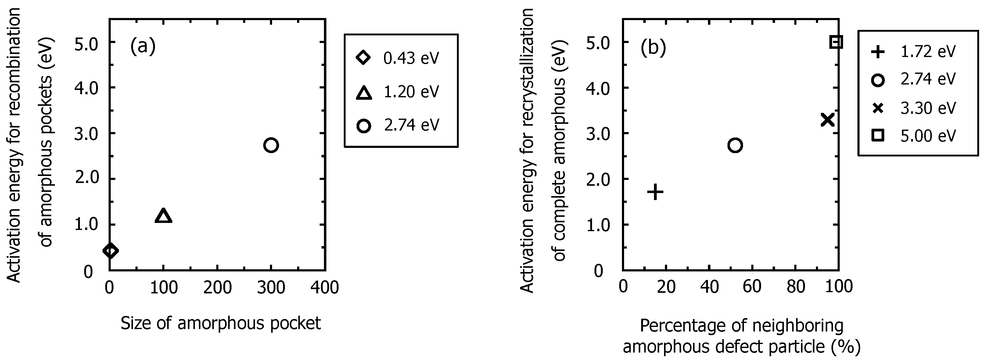
where is the recombination frequency, is the prefactor, is the amorphous pocket size, and is the calibration parameter for the size dependence. Also, is the activation energy for recombination, which depends on the size of the amorphous pockets, as shown in Figure 1a [13,27,29]. Linear interpolation is applied between the plots in Figure 1a. In addition, is the hydrostatic pressure and is the activation volume under that pressure. is the Boltzmann constant. is the absolute temperature of the subsequent thermal annealing treatment.
Furthermore, the recrystallization rate, , of complete amorphous regions was also calculated as
where is the parameter of the velocity prefactor. is the activation energy for SPEG. The activation energy for SPEG of complete amorphous regions is dependent on the percentage of neighboring amorphous , as shown in Figure 1b [13,30,31,32]. Moreover, is the activation volume under pressure. is the effect of other impurities. The recrystallization frequency, , of complete amorphous regions is defined as
where is the amorphous length in the direction of recrystallization. In the KMC algorithm, recrystallization is simulated from a set of random numbers and the recrystallization frequency of each amorphous state. The input values of each parameter for amorphization in MC ion implantation, the recombination of amorphous pockets in Equation (2), and the recrystallization of amorphous regions in Equation (3) are summarized in Table 1.

Table 1.
Input values of each parameter for amorphization in MC ion implantation, recombination of amorphous pockets in Equation (2), and recrystallization of amorphous regions in Equation (3).

Figure 1.
(a) The activation energy of amorphous pockets for recombination depends on the size [13,27,29]. (b) The activation energy of complete amorphous regions for recrystallization depends on the percentage of neighboring amorphous defect particles [13,31,32].
Figure 1.
(a) The activation energy of amorphous pockets for recombination depends on the size [13,27,29]. (b) The activation energy of complete amorphous regions for recrystallization depends on the percentage of neighboring amorphous defect particles [13,31,32].
3. Results and Discussion
3.1. Results of Analyzing Plan-View TEM Image of Si Substrate Surface after C3H5 Molecular Ion Implantation and Subsequent Thermal Annealing Treatment
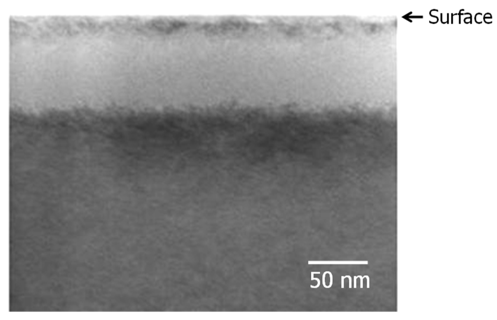
In this section, we show TEM images of the Si substrate surface after C3H5 molecular ion implantation and subsequent thermal annealing treatment and investigate preferential areas of initial rapid recrystallization by image analysis. Figure 2 shows cross-sectional bright-field TEM images of the Si substrate surface after C3H5 molecular ion implantation at a dose of 1.00 × 10¹⁵ ions/cm2 [13]. The buried amorphous layer is formed at a depth of 20–80 nm. The contrast of the TEM images indicates that some crystalline regions remain at a depth of 20 nm from the Si substrate surface. Figure 3 shows plan-view bright-field TEM images of the Si substrate surface after C3H5 molecular ion implantation. Here, the thickness of the plan-view TEM specimens is approximately 10 nm from the Si substrate surface. Hence, the plan-view TEM image is not affected by the buried amorphous layer inside. The size of the plan-view TEM image is 461 pixels × 610 pixels. In the plan-view TEM image of the C3H5-molecular-ion-implanted Si substrate surface, numerous discrete amorphous regions are formed. It is confirmed that many residual crystalline and discrete amorphous regions exist in the Si substrate surface; however, the amorphous/crystalline (A/C) interface is ambiguous. We obtained the gray level of every pixel in the plan-view TEM image using image process software.

Figure 2.
Cross-sectional bright-field TEM image of the Si substrate surface after C3H5 molecular ion implantation with dose of 1.00 × 10¹⁵ ions/cm2. Reproduced from Ref. [13].
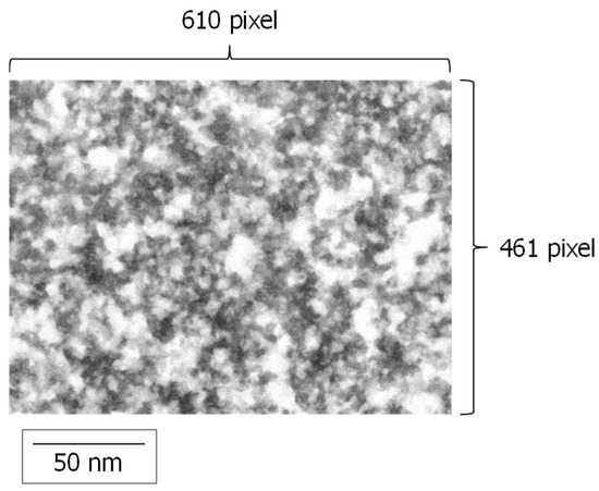
Figure 3.
Plan-view bright-field TEM image of the Si substrate surface after C3H5 molecular ion implantation with dose of 1.00 × 10¹⁵ ions/cm2.
Figure 4 shows the gray level distribution of the plan-view TEM image of the C3H5-molecular-ion-implanted Si substrate surface. In the bright-field TEM images, the crystalline regions are shown as dark contrast due to the diffraction of electron beams. On the other hand, owing to the transmission of electron beams, the amorphous regions are shown as bright contrast. Therefore, the contrast of the TEM image is considered an indicator of the crystallinity. As shown in Figure 4, the gray level distribution has three peaks in the near gray levels 100, 150, and 200. Then, in addition to the crystalline regions where the electron beam diffracts and is shown as a dark contrast and the amorphous region where the electron beam is transmitted and shown as a bright contrast, it can be seen that there are intermediate regions between the crystalline and amorphous regions, where electron beam transmission and diffraction occur simultaneously and are shown as gray contrast. Furthermore, from the peaks and bottoms of the gray level distribution in Figure 4, the contrast threshold values at which the crystalline, intermediate, and amorphous regions are predominant can be determined. There are many methods to determine threshold values [33]. In this study, the threshold values of the gray level distribution were determined using Otsu’s method [34]. In Otsu’s method, first, the gray level distribution is divided into three classes () by the threshold values and . The relationship between and is . To maximize , which is the variance between each class, the threshold values and are calculated as
where , , and are the occurrence probabilities of , , and , respectively.
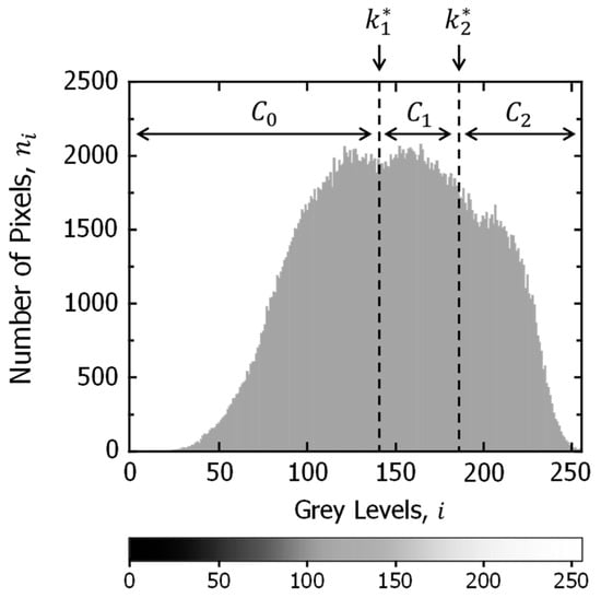
Figure 4.
Gray level distribution of the plan-view bright-field TEM image of the Si substrate surface after C3H5 molecular ion implantation.
Here, is gray level and is the number of pixels. is the total number of pixels. In addition, , , , and are the mean levels of the total and each class, which are calculated as
In this case, the extremely dark areas of the original TEM image impede the threshold value derivation, and and are searched at higher than gray level 95. As a result of the calculation, the threshold values and are obtained as 141 and 186, respectively. Using image processing software, we performed the image thresholding of the crystalline and intermediate phases using the threshold value from the plan-view TEM image. Then, the image thresholding of the crystalline and amorphous phases was also performed using the threshold value and superimposed on the image thresholding result of the threshold value . Finally, the crystalline–intermediate–amorphous phase map was created.
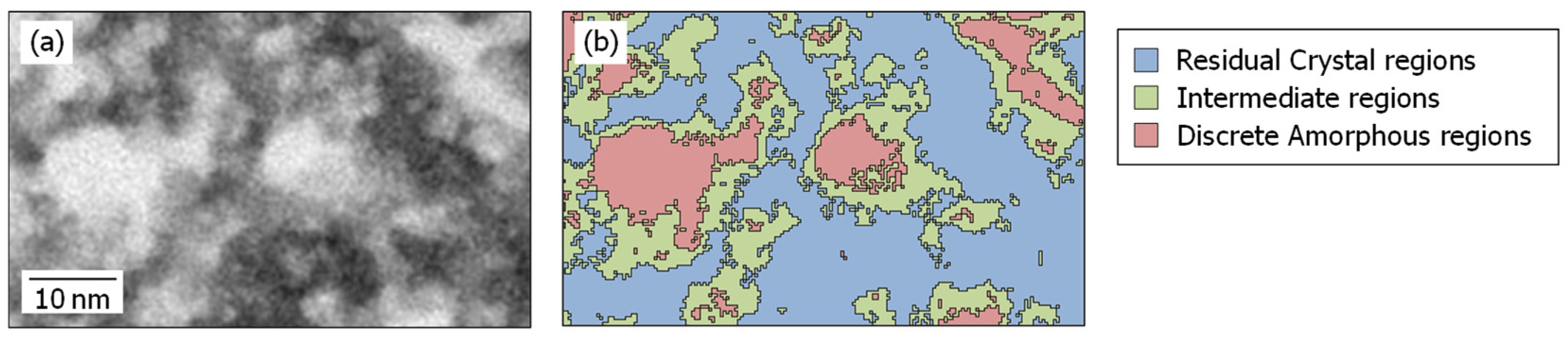
Figure 5 shows a set of the original plan-view TEM image and the crystalline–intermediate–amorphous phase map after C3H5 molecular ion implantation. In the phase map, the amorphous and intermediate regions are expressed as red and green islands, respectively, in the blue crystalline background. It is confirmed that crystalline, intermediate, and amorphous regions are represented in the phase map in accordance with the contrasts in the plan-view TEM image. It is seen that the complete amorphous regions are relatively circular, but the intermediate regions are formed into sharp shapes. It is found that all the discrete amorphous regions are surrounded by intermediate regions in the Si substrate surface after C3H5 molecular ion implantation.
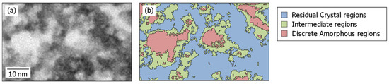
Figure 5.
Set of (a) the original plan-view bright-field TEM image and (b) crystalline–intermediate–amorphous phase map of Si substrate surface after C3H5 molecular ion implantation.
Next, we obtained the gray level distribution of the plan-view TEM image of the C3H5-molecular-ion-implanted Si substrate surface after subsequent thermal annealing (not shown) and confirmed that the peak position of the crystalline phase was unchanged. Then, using the same image thresholding procedure with the threshold values and , we obtained the phase map of the C3H5-molecular-ion-implanted Si substrate surface after subsequent thermal annealing treatment. Figure 6 shows a set of the original plan-view TEM image and the crystalline–intermediate–amorphous phase map of the C3H5 molecular-ion-implanted Si substrate surface after subsequent thermal annealing at 600 °C for 1 s. As shown in Figure 6, it seems that the size of the discrete amorphous region in the C3H5-molecular-ion-implaned Si substrate surface remains almost unchanged. However, it is found that the intermediate regions are recrystallized preferentially after subsequent thermal annealing treatment at 600 °C for 1 s.
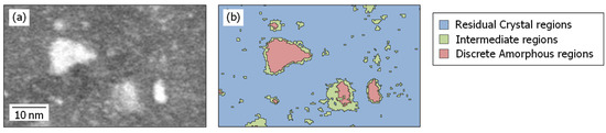
Figure 6.
Set of (a) the original plan-view bright-field TEM image and (b) crystalline–intermediate–amorphous phase map of C3H5-molecular-ion-implanted Si substrate surface after subsequent thermal annealing at 600 °C for 1 s.
As shown above, the recrystallization behavior of the intermediate region was significantly different from that of the complete amorphous region from the viewpoint of the plan-view TEM observation. In the next section, through MC ion implantation simulation, we calculate not only complete amorphous regions but also implant-induced isolated point defects and amorphous pockets. In addition, the recrystallization behavior of some amorphized states is also investigated by TCAD KMC process simulations.
3.2. TCAD Process Simulation Results after C3H5 Molecular Ion Implantation and Subsequent Thermal Annealing
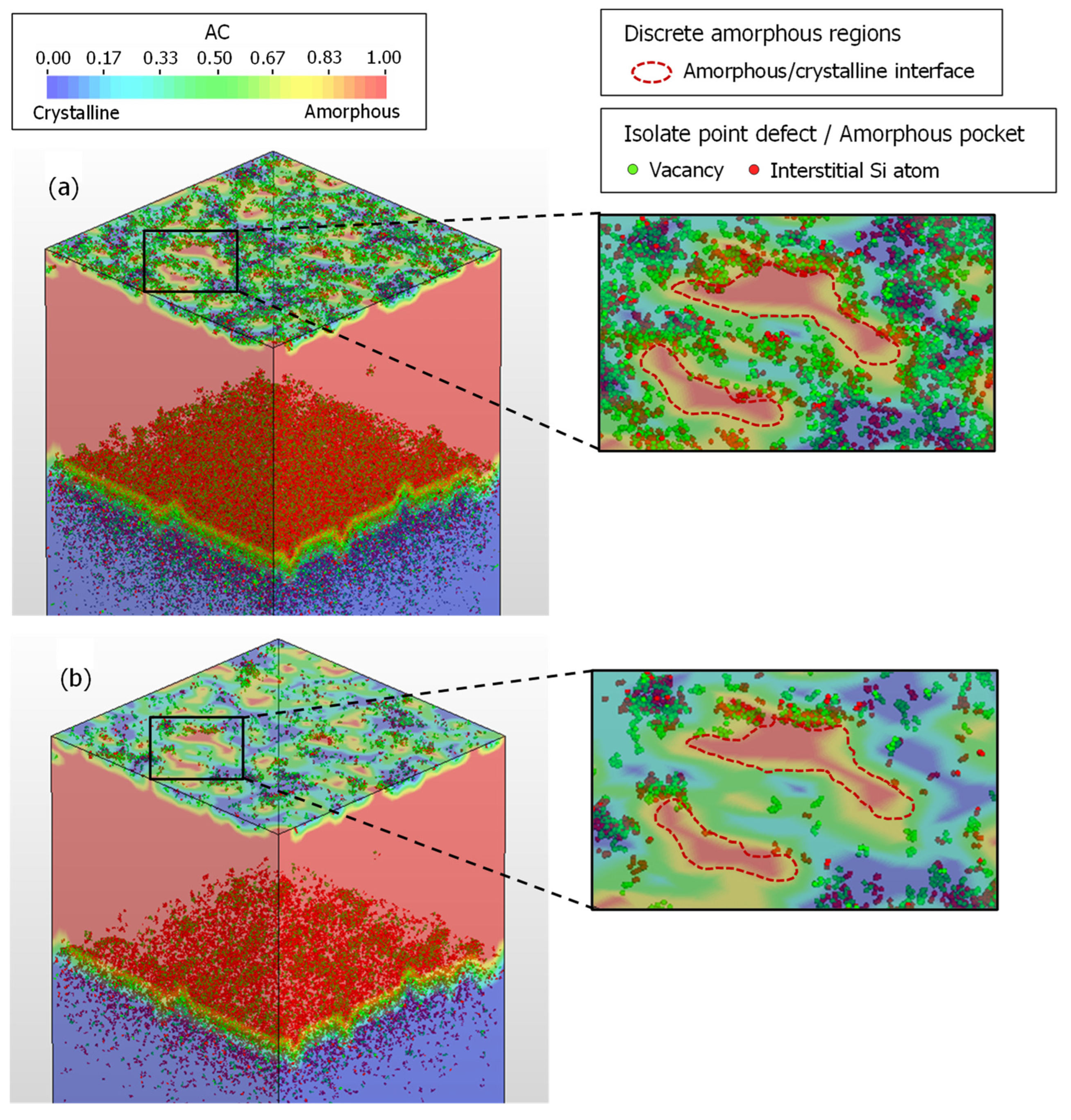
In this section, we use a TCAD process simulator to investigate the preferential areas for recrystallization in the discretely amorphized C3H5-molecular-ion-implanted Si substrate surface. Figure 7a shows the TCAD simulation model surface after C3H5 molecular ion implantation under the same ion implantation conditions as in the experiment. In Figure 7a, the crystallinity of the simulation model is represented by red to blue color contours using the AC parameter based on Equation (1). The TCAD simulation model shows that after C3H5 molecular ion implantation, the buried amorphous layer is formed at approximately the same depth as the cross-sectional TEM image in Figure 2. The A/C interface at the Si substrate surface is expressed by the red dotted line in the enlarged view of Figure 7a. The regions surrounded by the red line are discrete complete amorphous regions formed in the C3H5-molecular-ion-implanted simulation model. In addition, the implant-induced V and I as isolated point defects and in amorphous pockets are indicated by green and red particles, respectively, in the simulation model surface. As shown in the enlarged view of Figure 7a, it is found that the concentration of point defects in several small regions exceeds the amorphization threshold, and discrete complete amorphous regions are formed in the C3H5-molecular-ion-implanted simulation model surface. It is also seen that V and I as isolated point defects and in amorphous pockets are formed surrounding discrete complete amorphous regions in the simulation model surface after C3H5 molecular ion implantation. Thus, in the TCAD process simulation model shown in Figure 7a, the formation behavior of V and I as isolated point defects and in amorphous pockets corresponds to that in the intermediate regions shown in the phase map of the C3H5-molecular-ion-implanted Si substrate surface in Figure 5. Next, Figure 7b shows the discretely amorphized C3H5-molecular-ion-implanted simulation model surface after subsequent thermal annealing treatment at 600 °C for 1 s. In the enlarged view of Figure 7b, it is found that the number of V and I as isolated point defects and in amorphous pockets significantly decrease rapidly after subsequent thermal annealing for 1 s. It is also confirmed that the recrystallization behavior of V and I as isolated point defects and in amorphous pockets corresponds to the annihilation phenomena of the intermediate regions shown in the phase map of the C3H5-molecular-ion-implanted Si substrate surface after subsequent thermal annealing at 600 °C for 1 s in Figure 6.
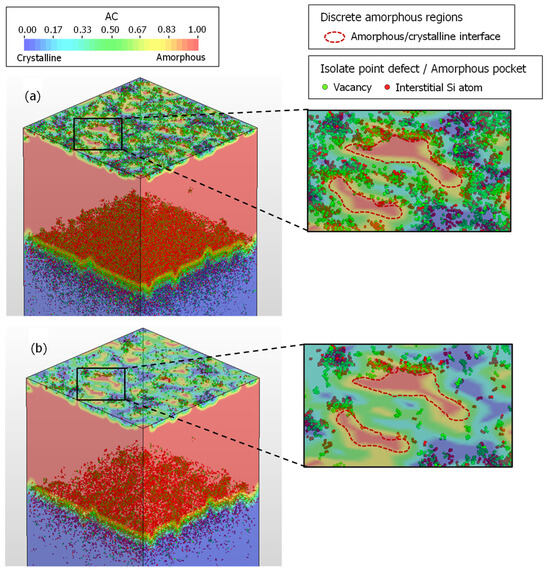
Figure 7.
Simulation model surface after (a) C3H5 molecular ion implantation and (b) subsequent thermal annealing at 600 °C for 1 s.
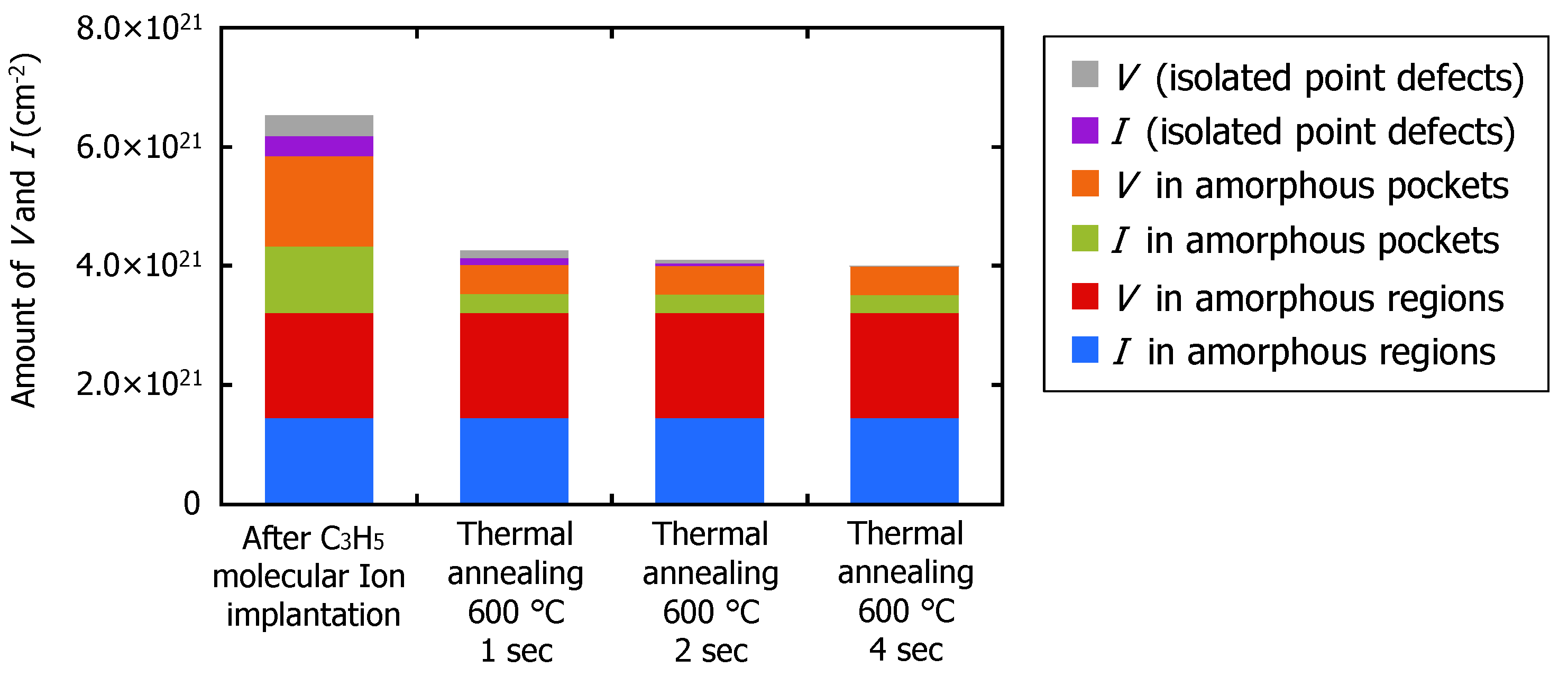
From the comparison of the results of the experimental plan-view TEM image analysis and TCAD simulation models, the intermediate regions shown in the phase maps are considered to be the regions where V and I as isolated point defects and in amorphous pockets are formed. In addition, Figure 8 shows the changes in the numbers of V and I as isolated point defects, in amorphous pockets, and in complete amorphous regions of the simulation model surface after C3H5 molecular ion implantation and subsequent thermal annealing at 600 °C for 1–4 s.
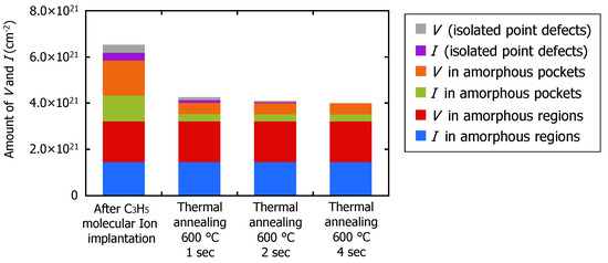
Figure 8.
Decreases in V and I as isolate point defects, in amorphous pockets, and in complete amorphous regions in simulation model surface after subsequent thermal annealing at 600 °C.
Here, the numbers of V and I of each amorphization status are counted within the depth of less than 3 nm from the simulation model surface. In Figure 8, it is found that the numbers of V and I as isolated point defects and in amorphous pockets of the simulation model surface are rapidly reduced by subsequent thermal annealing for 1–4 s. It is also seen that decreases in the numbers of V and I, as isolate point defects and in amorphous pockets, become smaller with longer thermal annealing time. Therefore, to evaluate the crystallinity quantitatively, the change in the crystalline fraction of the C3H5-molecular-ion-implanted Si substrate surface after subsequent thermal annealing is determined as
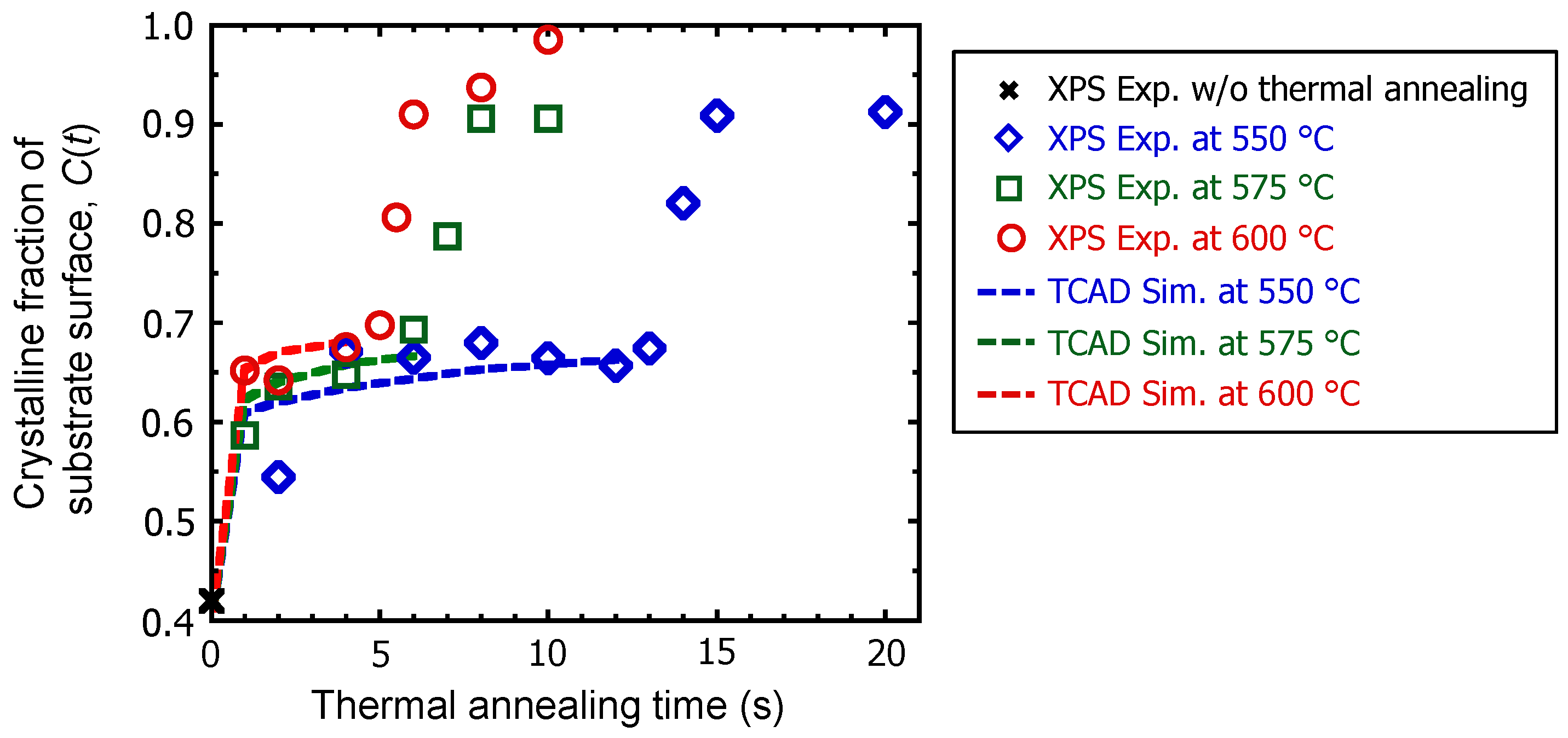
where and , , and are, respectively, the concentrations of V and I as isolated point defects and in amorphous pockets. is the fitting parameter for the ratio of amorphous pockets and amorphous regions. Figure 9 shows the change in the crystalline fraction of the discretely amorphized C3H5-molecular-ion-implanted Si substrate surface after subsequent thermal annealing at 550 °C, 575 °C, and 600 °C.
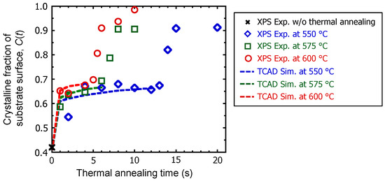
Figure 9.
Crystalline fractions in C3H5-molecular-ion-implanted Si substrate surface with subsequent thermal annealing at 550 °C, 575 °C, and 600 °C determined from experimental results of XPS and TCAD simulation results, due to recrystallization of amorphous pockets.
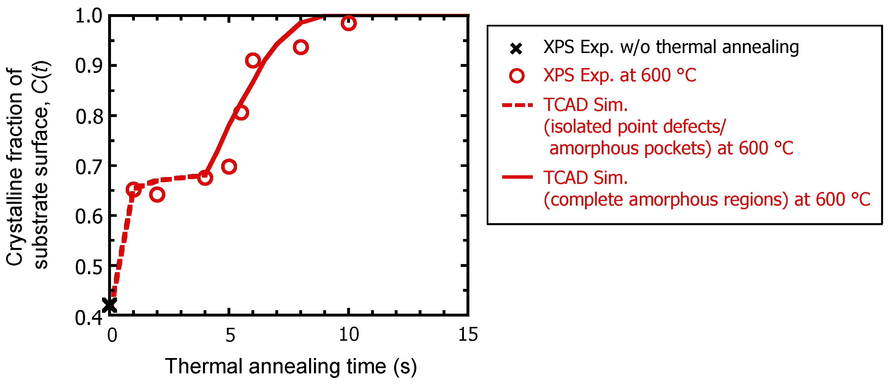
The experimental values in Figure 9 are quantitatively derived from the shape of the XPS Si 2p spectra of the Si substrate surface after C3H5 molecular ion implantation and subsequent thermal annealing in the previous work [13]. In the experimental result of XPS, in the 1st step of recrystallization, the crystalline fraction of the Si substrate surface rapidly increases during subsequent thermal annealing at 550 °C, 575 °C, and 600 °C for approximately 1–4 s. Then, after the 1st step and the incubation periods, the crystalline fraction increases again following a sigmoidal curve in the 2nd step. The results of the TCAD process simulation indicate that the change in the crystalline fraction of the C3H5-molecular-ion-implanted Si substrate surface due to the recrystallization of V and I as isolated point defects and in amorphous pockets corresponds to the initial rapid recrystallization behavior in the 1st step revealed by the experimental XPS analysis results. Furthermore, we hypothesize that after the recrystallization of V and I as isolated point defects and in amorphous pockets in the 1st step, the recrystallization of discrete complete amorphous regions starts in the 2nd step. Thus, we conducted a two-step recrystallization simulation. Figure 10 shows the results of the two-step recrystallization simulation of the 1st step (isolated point defect and amorphous pockets) and 2nd step (complete amorphous regions). As shown in Figure 10, the two-step recrystallization simulation results agree with the experimental results of the XPS analysis entirely. Therefore, as mentioned above, there is an order of recrystallizing regions in the discretely amorphized Si substrate surface. We believe that the isolated point defects and amorphous pockets (i.e., intermediate regions) are first recrystallized in the 1st step as the preferential areas, and then the complete amorphous regions formed discretely are recrystallized in the 2nd step. In the next section, we describe the overall two-step recrystallization model of the discretely amorphous C3H5-molecular-ion-implanted Si substrate surface.
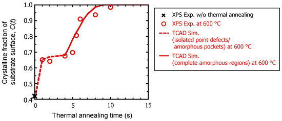
Figure 10.
Crystalline fractions in C3H5-molecular-ion-implanted Si substrate surface with subsequent thermal annealing at 600 °C determined from experimental results of XPS and TCAD simulation results due to recrystallization of amorphous pockets and complete amorphous regions.
3.3. Overall Two-Step Recrystallization Model of the Discretely Amorphized C3H5-Molecular-Ion-Implanted Si Substrate Surface
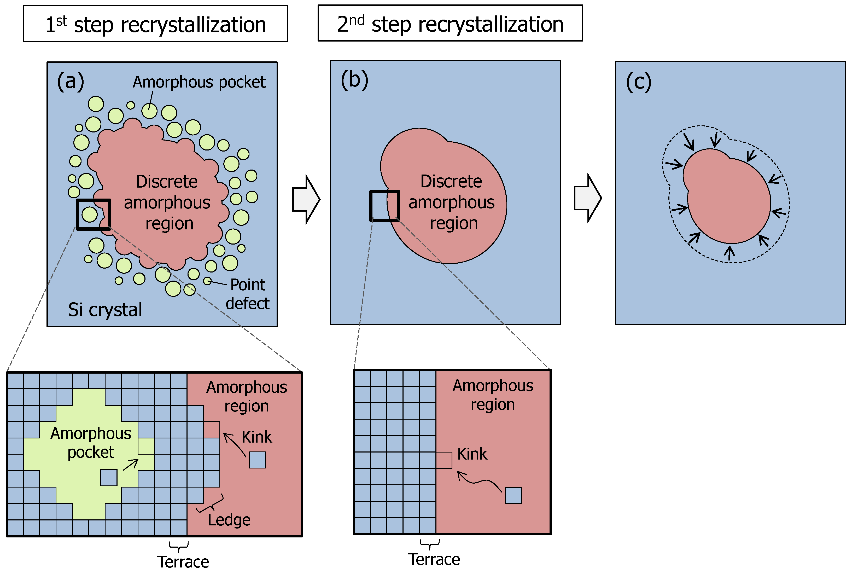
Figure 11 shows a schematic diagram of the overall two-step recrystallization model of the discretely amorphized C3H5-molecular-ion-implanted Si substrate surface. As shown in Figure 11a, isolated point defects and amorphous pockets are formed around the discrete amorphous regions in the C3H5-molecular-ion-implanted Si substrate surface. Regarding the relationship between the amorphous pockets and complete amorphous regions, Edmondson et al. previously reported that amorphous regions are formed heterogeneously because of overlapping amorphous pockets [35]; therefore, it is considered that discrete complete amorphous regions are always surrounded by amorphous pockets. For the same reason, the A/C interface of a discrete amorphous region is rough after C3H5 molecular ion implantation. In the enlarged view of Figure 11a, the atomistic image shows the SPEG behavior of the A/C interface. As described in previous papers, SPEG behavior was explained simply by the motion of terraces, ledges, and kinks at the A/C interface [36,37,38,39]. In these papers, the Si atom from the amorphous region was hypothesized to be trapped at the A/C interface as a kink, then the connected kinks formed a ledge, the stacked ledges further created a planar terrace, and SPEG proceeded via the layer-by-layer growth of the terrace. In the 1st recrystallization step, a ledge is already formed at amorphous pockets and the rough A/C interface. A kink is easily trapped in the existing ledge and SPEG rapidly proceeds. Because the 1st recrystallization step continues until preferential areas such as amorphous pockets and the rough of the A/C interface are consumed, the change in the crystalline fraction shows an initial rapid reaction and incubation periods. Then, as shown in the enlarged views of Figure 11b in the 2nd recrystallization step, since there are no isolated point defects, amorphous pockets, or rough A/C interface, the kinks must form a ledge at the terrace without any assistance part. In previous articles, many authors showed the initial rapid SPEG and plateau behavior due to the recombination of amorphous pockets through experiments [40,41,42] and molecular dynamic simulation [29]. In this study, we clearly observed a relationship between the 1st recrystallization step of the amorphous pockets and the 2nd recrystallization step of the complete amorphous regions in the Si substrate surface.
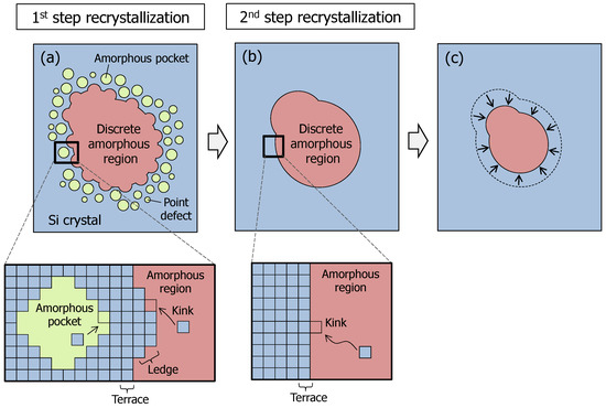
Figure 11.
Two-step recrystallization model of discretely amorphized C3H5-molecular-ion-implanted Si substrate surface. (a) Isolated point defects and amorphous pockets are formed around the discrete amorphous regions after the C3H5 molecular ion implantation. In addition, the A/C interface of a discrete amorphous region is rough. In the 1st recrystallization step, a kink is trapped in ledge formed at amorphous pockets and the rough A/C interface and SPEG rapidly proceeds. Until preferential areas such as amorphous pockets and the rough of the A/C interface are consumed, the 1st recrystallization step continues. (b) In the 2nd recrystallization step, the kinks must form a ledge at the terrace without assistance part. (c) SPEG proceeds slowly via layer-by-layer from the outside.
It has also been reported that the formation behavior of amorphous pockets is significantly affected by the mass of the ion-implanted species, acceleration energy, and Si substrate temperature [43]. Then, to optimize the subsequent thermal annealing conditions after C3H5 molecular ion implantation, it is necessary to perform a preliminary estimation of not only the complete amorphous regions but also the amorphous pockets formed on the Si substrate surface.
4. Conclusions
The initial rapid recrystallization of preferential areas in a discretely amorphized C3H5-molecular-ion-implanted Si substrate surface was analyzed through the analysis of plan-view TEM images and TCAD process simulation. We obtained a crystalline–intermediate–amorphous phase map using the thresholding plan-view TEM image of the Si substrate surface after C3H5 molecular ion implantation and subsequent thermal annealing. We found that the initial rapid recrystallization occurred in the intermediate regions around discrete amorphous regions formed in the C3H5-molecular-ion-implanted Si substrate surface. In addition, the TCAD process simulation results indicated that the formation and recrystallization behavior of the amorphous pockets around discrete amorphous regions corresponds to the intermediate regions of the phase map. Furthermore, it was confirmed that the change in the crystalline fraction of the Si substrate surface due to the recrystallization of amorphous pockets and discrete complete amorphous regions in the TCAD process simulation corresponds quantitatively to that of the experimental XSP analysis results. Thus, the recrystallization of the C3H5-molecular-ion-implaned Si substrate surface proceeds via two steps. After the initial recrystallization of amorphous pockets in the 1st step, the recrystallization of discrete amorphous regions starts in the 2nd step. The incubation period between the 1st and 2nd steps is assumed to be the time required for the complete recombination of the amorphous pocket and the redefinition of the A/C interface.
Author Contributions
Conceptualization, K.K. (Koji Kobayashi), R.O., T.K., A.O.-M., R.H., A.S., Y.K., K.S. and K.K. (Kazunari Kurita); methodology, K.K. (Koji Kobayashi), R.O. and T.K.; software, K.K. (Koji Kobayashi), R.O. and R.H.; validation, K.K. (Koji Kobayashi); formal analysis, K.K. (Koji Kobayashi); investigation, K.K. (Koji Kobayashi); resources, K.K. (Koji Kobayashi), T.K. and K.K. (Kazunari Kurita); data curation, K.K. (Koji Kobayashi), R.O., T.K., A.O.-M., R.H., A.S., Y.K., K.S. and K.K. (Kazunari Kurita); writing—original draft preparation, K.K. (Koji Kobayashi); writing—review and editing, K.K. (Koji Kobayashi), K.S. and K.K. (Kazunari Kurita); visualization, K.K. (Koji Kobayashi); supervision, K.K. (Kazunari Kurita); project administration, K.K. (Kazunari Kurita). All authors have read and agreed to the published version of the manuscript.
Funding
This research received no external funding.
Data Availability Statement
The data presented in this study are available upon request from the corresponding author. The data are not publicly available due to privacy and confidentiality concerns.
Acknowledgments
The authors would like to express their gratitude to Hisashi Furuya and Naoki Ikeda of SUMCO Corporation for their great encouragement and management support in the research activities.
Conflicts of Interest
The authors declare no conflicts of interest. Author Koji Kobayashi, Ryosuke Okuyama, Takeshi Kadono, Ayumi Onaka-Masada, Ryo Hirose, Akihiro Suzuki, Yoshihiro Koga, Kazunari Kurita were employed by the company SUMCO Corporation (Japan). The remaining authors declare that the research was conducted in the absence of any commercial or financial relationships that could be construed as a potential conflict of interest.
References
- Russo, F.; Nardone, G.; Polignano, M.L.; D’Ercole, A.; Pennella, F.; Felice, M.D.; Monte, A.; Matarazzo, A.; Moccia, G.; Polsinelli, G.; et al. Dark Current Spectroscopy of Transition Metals in CMOS Image Sensors. ECS J. Solid State Sci. Technol. 2017, 6, 217–226. [Google Scholar] [CrossRef]
- Domengie, F.; Regolini, J.L.; Bauza, D. Study of metal contamination in CMOS image sensors by dark-current and deep-level transient spectroscopies. J. Electron. Mater. 2010, 39, 625–629. [Google Scholar] [CrossRef]
- Ohtani, A.; Kaneda, T. Analysis of residual image in CMOS image sensor 2. In Proceedings of the Extended Abstracts of the 77th Japan Society of Applied Physics and Related Societies Autumn Meeting, Niigata, Japan, 13–16 September 2016; p. 14p-P6-11. (In Japanese). [Google Scholar]
- Tournier, A.; Leverd, F.; Favennec, L.; Perrot, C.; Pinzelli, L.; Gatefait, M.; Cherault, N.; Jeanjean, D.; Carrere, J.-P.; Hirigoyen, F.; et al. Pixel-to-pixel isolation by deep trench technology: Application to CMOS image sensor. In Proceedings of the 2011 International Image Sensor Workshop (IISW), Hokkaido, Japan, 8–11 June 2011; pp. 12–15. [Google Scholar]
- Kwon, H.I.; Kang, I.M.; Park, B.G.; Lee, J.D.; Park, S.S. The analysis of dark signals in the CMOS APS imagers from the characterization of test structures. IEEE Trans. Electron Devices 2004, 51, 178–184. [Google Scholar] [CrossRef]
- Kurita, K.; Kadono, T.; Okuyama, R.; Onaka-Masada, A.; Shigematsu, S.; Kobayashi, K.; Suzuki, A.; Okuda, H.; Koga, Y. Silicon Wafer Gettering Design for Advanced CMOS Image Sensors Using Hydrocarbon Molecular Ion Implantation: A Review. IEEE J. Electron Devices Soc. 2021, 10, 720–727. [Google Scholar] [CrossRef]
- Kurita, K.; Kadono, T.; Okuyama, R.; Hirose, R.; Onaka-Masada, A.; Koga, Y.; Okuda, H. Proximity gettering of C3H5 carbon cluster ion-implanted silicon wafers for CMOS image sensors: Gettering effects of transition metal, oxygen, and hydrogen impurities. Jpn. J. Appl. Phys. 2016, 55, 121301. [Google Scholar] [CrossRef]
- Kurita, K.; Kadono, T.; Okuyama, R.; Shigematsu, S.; Hirose, R.; Onaka-Masada, A.; Koga, Y.; Okuda, H. Proximity gettering technology for advanced CMOS image sensors using carbon cluster ion-implantation technique: A review. Phys. Status Solidi A 2017, 214, 1700216. [Google Scholar] [CrossRef]
- Okuda, H.; Okuyama, R.; Iwanaga, T.; Kadono, T.; Hirose, R.; Koga, Y.; Kurita, K. Proximity Gettering of Carbon Cluster Ion Irradiated Silicon Wafers (3)—Oxygen Diffusion Behavior after Epitaxial Growth. In Proceedings of the Extended Abstracts of the 62nd Japan Society of Applied Physics and Related Societies Spring Meeting, Kanagawa, Japan, 11–14 March 2015; p. 12p-A18-15. (In Japanese). [Google Scholar]
- Okuyama, R.; Masada, A.; Kadono, T.; Hirose, R.; Koga, Y.; Okuda, H.; Kurita, K. Trapping and diffusion kinetic of hydrogen in carbon-cluster ion-implantation projected range in Czochralski silicon wafers. Jpn. J. Appl. Phys. 2017, 56, 025601. [Google Scholar] [CrossRef]
- Kadono, T.; Okuyama, R.; Onaka-Masada, A.; Hirose, R.; Shigematsu, S.; Koga, Y.; Okuda, H.; Kurita, K. Effect of hydrocarbon molecular ion size for amorphous region formation analyzed by X-ray photoelectron spectroscopy. Jpn. J. Appl. Phys. 2020, 59, 025510. [Google Scholar] [CrossRef]
- Kobayashi, K.; Okuyama, R.; Kadono, T.; Onaka-Masada, A.; Hirose, R.; Shigematsu, S.; Suzuki, A.; Koga, Y.; Kurita, K. Re-crystallization Behavior of Amorphous Layer in Hydrocarbon Molecular Ion Implanted Region Using Flash Lamp Annealing. In Proceedings of the 2018 22nd International Conference on Ion Implantation Technology (IIT), Würzburg, Germany, 16–21 September 2018; pp. 357–360. [Google Scholar]
- Kobayashi, K.; Okuyama, R.; Kadono, T.; Onaka-Masada, A.; Hirose, R.; Suzuki, A.; Koga, Y.; Kurita, K. Recrystallization model of discrete amorphous regions in C3H5-molecular-ionimplanted silicon substrate surface analyzed by X-ray photoelectron spectroscopy. Jpn. J. Appl. Phys. 2022, 61, 115501. [Google Scholar] [CrossRef]
- Kobayashi, K.; Okuyama, R.; Kadono, T.; Onaka-Masada, A.; Hirose, R.; Suzuki, A.; Koga, Y.; Kurita, K.; Sueoka, K. Kinetic Monte Carlo Simulations for Recrystallization Process of Discrete Amorphous Regions in C3H5-Molecular-Ion-Implanted Silicon Substrate Surface. In Proceedings of the 2023 21st International Workshop on Junction Technology (IWJT), Kyoto, Japan, 8–9 June 2023; pp. 140–143. [Google Scholar]
- Kobayashi, K.; Okuyama, R.; Kadono, T.; Onaka-Masada, A.; Hirose, R.; Suzuki, A.; Koga, Y.; Sueoka, K.; Kurita, K. Two-and three-dimensional recrystallization of discrete amorphous in C3H5-molecular-ion-implanted silicon surface analyzed by TCAD simulation. ECS J. Solid State Sci. Technol. 2023. submitted. [Google Scholar]
- Johnson, W.A.; Mehl, R.F. Reaction Kinetics in Processes of Nucleation and Growth. Trans. Am. Inst. Min. Metall. Eng. 1939, 135, 416–442. [Google Scholar]
- Avrami, M. Kinetics of Phase Change. I General theory. J. Chem. Phys. 1939, 7, 1103–1112. [Google Scholar] [CrossRef]
- Avrami, M. Kinetics of Phase Change. II transformation-time relations for random distribution of nuclei. J. Chem. Phys. 1940, 8, 212–224. [Google Scholar] [CrossRef]
- Avrami, M. Granulation, phase change, and microstructure kinetics of phase change. III. J. Chem. Phys. 1941, 9, 177–184. [Google Scholar] [CrossRef]
- Yamamoto, M. Kinetics of Material; Uchida Rokakuho: Tokyo, Japan, 2015; Chapter 3; pp. 145–148. [Google Scholar]
- Yoo, W.S.; Ishigaki, T.; Kang, K. Image processing software assisted quantitative analysis of various digital images in process monitoring, process control and material characterization. In Proceedings of the 2017 International Conference on Frontiers of Characterization and Metrology for Nanoelectronics (ICFCMN), Monterey, CA, USA, 20–23 March 2017; pp. 276–279. [Google Scholar]
- Synopsys Sentaurus Process User’s Manual, Release p-2019.03; Synopsys Inc.: Zurich, Switzerland, 2019; pp. 104–128, 433–442, 455–464.
- Tian, S. Predictive Monte Carlo ion implantation simulator from sub-keV to above 10 MeV. J. Appl. Phys. 2003, 93, 5893–5904. [Google Scholar] [CrossRef]
- Posselt, M.; Schmidt, B.; Murthy, C.S.; Feudel, T.; Suzuki, K. Modeling of Damage Accumulation during Ion Implantation into Single-Crystalline Silicon. J. Electrochem. Soc. 1997, 144, 1495–1504. [Google Scholar] [CrossRef]
- Bragado, M.; Borges, R. Kinetic Monte Carlo simulation for semiconductor processing: A review. Prog. Mater. Sci. 2018, 92, 1–32. [Google Scholar] [CrossRef]
- Battaglia, A.; Priolo, F.; Rimini, E.; Ferla, G. Ion-induced annealing and amorphization of isolated damage clusters in Si. Appl. Phys. Lett. 1990, 56, 2622–2624. [Google Scholar] [CrossRef]
- Donnelly, S.E.; Bircher, R.C.; Vishnyakov, V.M.; Carter, G. Annealing of isolated amorphous zones in silicon. Appl. Phys. Lett. 2003, 82, 1860–1862. [Google Scholar] [CrossRef]
- Caturla, M.-J.; Diaz de la Rubia, T.; Marques, L.A.; Gilmer, G.H. Ion-beam processing of silicon at keV energies: A molecular-dynamics study. Phys. Rev. B. 1996, 54, 16683. [Google Scholar] [CrossRef]
- Mok, K.R.C.; Benistant, F.; Jaraiz, M.; Rubio, J.E.; Castrillo, P.; Pinacho, R.; Srinivasan, M.P. Comprehensive model of damage accumulation in silicon. J. Appl. Phys. 2008, 103, 014911. [Google Scholar] [CrossRef]
- Pelaz, L.; Marques, L.A.; Aboy, M.; Barbolla, J.; Gilmer, G.H. Atomistic modeling of amorphization and recrystallization in silicon. Appl. Phys. Lett. 2003, 82, 2038–2040. [Google Scholar] [CrossRef]
- López, P.; Pelaz, L.; Marqués, L.A.; Santos, I. Atomistic analysis of the annealing behavior of amorphous regions in silicon. J. Appl. Phys. 2007, 101, 093518. [Google Scholar] [CrossRef]
- Masaki, Y.; LeComber, P.G.; Fitzgerald, A.G. Solid phase crystallization of thin films of Si prepared by plasma-enhanced chemical vapor deposition. J. Appl. Phys. 1993, 74, 129–134. [Google Scholar] [CrossRef]
- Sezgin, M.; Sankur, B. Survey over image thresholding techniques and quantitative performance evaluation. J. Electron. Imaging. 2004, 13, 146–168. [Google Scholar]
- Otsu, N. A Threshold Selection Method from Gray-Level Histograms. IEEE Trans. Syst. Man Cybern. 1979, 9, 62–66. [Google Scholar] [CrossRef]
- Edmondson, P.D.; Riley, D.J.; Birtcher, R.C.; Donnelly, S.E. Amorphization of crystalline Si due to heavy and light ion irradiation. J. Appl. Phys. 2009, 106, 043505. [Google Scholar] [CrossRef]
- Csepregi, L.; Kennedy, E.F.; Mayer, J.W.; Sigmon, T.W. Substrate-orientation dependence of the epitaxial regrowth rate from Si-implanted amorphous Si. J. Appl. Phys. 1978, 49, 3906–3911. [Google Scholar] [CrossRef]
- Spaepen, F.; Turnbull, D. Laser Annealing of Semiconductor; Academic Press: New York, NY, USA, 1982; Chapter 2; pp. 28–31. [Google Scholar]
- Williams, J.S.; Elliman, R.G. Role of electronic processes in epitaxial recrystallization of amorphous semiconductors. Phys. Rev. Lett. 1983, 51, 1069. [Google Scholar] [CrossRef]
- Lu, G.-W.; Nygren, E.; Aziz, M.J. Pressure-enhanced crystallization kinetics of amorphous Si and Ge: Implications for point-defect mechanisms. J. Appl. Phys. 1991, 70, 5323–5345. [Google Scholar] [CrossRef]
- Priolo, F.; Battaglia, A.; Nicotra, R.; Rimini, E. Low-temperature reordering in partially amorphized Si crystals. Appl. Phys. Lett. 1990, 57, 768–770. [Google Scholar] [CrossRef]
- Donnelly, S.E.; Birtcher, R.C.; Vishnyakov, V.M.; Edmondson, P.D.; Carter, G. Anomalous annealing behavior of isolated amorphous zones in silicon. Nucl. Instr. Meth. Phys. Res. B 2006, 242, 595–597. [Google Scholar] [CrossRef]
- El-Ghor, M.K.; Holland, O.W.; White, C.W.; Pennycook, S.J. Structural characterization of damage in Si (100) produced by MeV Si+ ion implantation and annealing. J. Mater. Res. 1990, 5, 352–359. [Google Scholar] [CrossRef]
- Holland, O.W.; White, C.W.; El-Ghor, M.K.; Budai, J.D. MeV, self-ion implantation in Si at liquid nitrogen temperature; a study of damage morphology and its anomalous annealing behavior. J. Appl. Phys. 1990, 68, 2081–2086. [Google Scholar] [CrossRef]


Disclaimer/Publisher’s Note: The statements, opinions and data contained in all publications are solely those of the individual author(s) and contributor(s) and not of MDPI and/or the editor(s). MDPI and/or the editor(s) disclaim responsibility for any injury to people or property resulting from any ideas, methods, instructions or products referred to in the content. |
© 2024 by the authors. Licensee MDPI, Basel, Switzerland. This article is an open access article distributed under the terms and conditions of the Creative Commons Attribution (CC BY) license (https://creativecommons.org/licenses/by/4.0/).