Article

High-Conductivity MXene Film-Based Millimeter Wave Antenna for 5G Applications

1
Hubei Engineering Research Center of RF-Microwave Technology and Application, School of Science, Wuhan University of Technology, Wuhan 430070, China
2
Hainan Research Institute, Wuhan University of Technology, Sanya 572000, China
3
School of Information Engineering, Wuhan University of Technology, Wuhan 430070, China
4
State Key Laboratory of Advanced Technology for Materials Synthesis and Processing, Center of Smart Materials and Devices, Wuhan University of Technology, Wuhan 430070, China
*
Authors to whom correspondence should be addressed.
These authors contributed equally to this work.
Crystals 2023, 13(7), 1136; https://doi.org/10.3390/cryst13071136
Submission received: 21 June 2023 / Revised: 9 July 2023 / Accepted: 14 July 2023 / Published: 21 July 2023
(This article belongs to the Section Materials for Energy Applications)

Abstract

:
Millimeter wave antennas have the advantage of high directivity, miniaturization, high resolution and data transfer speed, wide bandwidth, and lower latency. In this work, a millimeter wave planar array antenna (PAA) with the characteristics of wideband and low sidelobes, which consists of eight identical linear array antenna (LAA) based on Ti3C2 MXene, is designed and fabricated. It is the first time that MXene antennas are proposed for a 5G millimeter wave antenna application. MXene PAA has a high realized gain of 22.22 dBi and a −10 dB impedance bandwidth of measurement covering the range from 24 GHz to 28 GHz, including the 5G FR2—n258 frequency band. With Chebyshev current distribution, the MXene PAA has a half-power beam width of 10.2° and 10.8° in the xoz-plane and yoz-plane radiation patterns with the sidelobes levels below −20 dB, respectively. Therefore, MXene PAA is suitable for 5G mobile communication applications.

1. Introduction

With the advancement of the large-scale commercial implementation of the fifth-generation (5G) communication systems around the world, the 5G millimeter wave (MMW) communication has become a current research hotspot [1,2,3]. In 2019, the International Telecommunication Union (ITU) determined spectrum resources of 24.25 GHz–27.5 GHz, 37 GHz–43.5 GHz and 66 GHz–76 GHz for 5G and the future development of international mobile telecommunications (IMT) [4]. MMW has the peculiarities of low latency, high data transmission and high speed, which can be widely used in medical livelihood, health checkups, virtual reality and other fields [5,6].
The antenna is a significant component of 5G communication systems [7]. High gain array antenna has become a practical technical approach to solve the high loss of millimeter wave in free space [8]. Owing to the rapid advancement of the modern electronics industry, antennas for 5G are evolving in the direction of high gain, light weight and easy conformability [9]. Traditional antennas are mostly made of metal with high density, poor mechanical properties and easy corrosion, which cannot meet the requirement of 5G communication systems. Advanced conductive materials have been used extensively in radio frequency (RF) devices in recent years [10,11,12], which have shown improved properties than most metals due to the excellent mechanical properties, lightweight and adaptability in complex environments [13,14,15,16].
Two-dimensional titanium carbide (Ti3C2 MXene) is a new two-dimensional material with good flexibility, hydrophilicity, and high metalloid conductivity [17,18]. The precursor MAX phase of MXene is a class of compounds with a densely arranged hexagonal ternary layered structure with the chemical formula Mn+1AXn (n = 1, 2, 3), where M is a pre-transition metal (Ti, V, Zr, Nb, etc.), A stands for an III or IV main group element (Al, Ga, In, Ti, Si, etc.) and X represents carbon or nitrogen. In 2011, Gogotsi obtained the two-dimensional crystalline material Ti3C2Tx by selectively etching the Al atomic layer in Ti3AlC2 by HF [19]. The new two-dimensional nanomaterial has a theoretical monolayer thickness of 1 nm and has a similar structure compared with graphene, leading to the name MXene. Since being discovered by Gogotsi, MXene has significantly impacted materials science and nanotechnology. For the characteristics of good electrical properties and excellent mechanical properties [20,21], Ti3C2 MXene is becoming a popular material in RF [22,23,24,25,26]. For instance 2018, Gogotsi et al. successfully fabricated a 100 nm-thick translucent dipole antenna operating on the Wi-Fi frequency band (2.4 GHz) for the first time by spraying MXene ink [22]. In 2022, Zhao et al. built a full MXene printing integrated system under room temperature to realize ultrafine-printed (3 μm line gap) [25]. The unencapsulated MXene NFC antenna is still functional after two years in low-temperature storage. In the same year, Huang et al. proposed an MXene ultrawideband antenna [26], which covers WLAN, Bluetooth, and 5G bands which is the first time to transmit a film wirelessly using by MXene antenna. Researchers have extensive research based on MXene materials in RF communications and have achieved excellent results, offering a reference benchmark for latecomers. However, most works focus on researching fabrication methods, while the antenna structure is simple. There are no antenna applications based MXene in the MMW frequency band, and the application of MXene antenna for 5G communication is being explored.
Herein, we propose an MMW planar array antenna with wideband and low sidelobes based on high-conductivity MXene film for 5G mobile communication for the first time. Firstly, an MXene linear array antenna (LAA) with Chebyshev current distribution was designed to operate at 26 GHz, conforming to the requirements of the 5G FR2—n258 communication band. The measured −10 dB impedance bandwidth of the MXene linear array antenna covers 25.21 GHz to 26.92 GHz. Then, the MXene planar array antenna (PAA) based on the eight identical LAAs shows good broadband characteristics which −10 dB bandwidth of measurement is covering the 5G MMW communication frequency band. In the xoz-plane and yoz-plane, the sidelobes levels of the MXene planar array antenna radiation patterns are lower than −20 dB with the half power beam width of 10.2° and 10.8°, respectively. The proposed MXene MMW array antenna reveals the enormous potential for MXene materials in 5G communication, which offers significant application perspectives for radar, unmanned driving, 5G communication and other typical MMW applications required in the future.

2. Materials and Methods

2.1. Preparation of High-Conductivity MXene Film

MXene (Ti3C2) was synthesized by selectively etching the Al atomic layer from the corresponding precursor MAX phase (Ti3AlC2) [16]. The sediment was washed several times with DI water to neutralize the acidic pH and occurred self-delamination. Then, the dark green supernatant was collected and obtained high-concentration MXene nanosheets by high-speed centrifugation [27]. After homogenizing and degassing, 60 mg mL−1 MXene ink was poured on the commercial single-layer polypropylene film (Celagrd 3501), and the height of the blade was adapted to 750 μm with the rate of movement in 20 cm S−1. Finally, the large-area MXene ink was dried to MXene film (a thickness of 16 μm) at room temperature, overnight.
In order to acquire the accurate conductivity of MXene film that we prepared, the sheet resistance of MXene films was measured by a four-probe tester. Four probes made of tungsten wires were arranged in straight lines at equal intervals. When the film is measured, the tip of the needle is pressed onto the surface of MXene film. Then, two external probes were energized and two internal probes were used to measure the potential difference to obtain the sheet resistance of the MXene film. Then, the conductivity of MXene film can be calculated according to the equation in [28]:
σ = 1 ρ
  ρ = 1 R s   ×   t
where the conductivity is   σ , the electrical resistivity is ρ , the sheet resistance is R s , the thickness of film is t.
The thickness of MXene film is 16 μm with the sheet resistance of 0.017 Ω / sq (the unit of the sheet resistance of MXene film is Ω / sq ) . Therefore, the conductivity value of MXene film is approximately 3.5 × 10⁵ S/m. In a summary, MXene film demonstrates superior conductivity, offering a promising prospect in antenna design

2.2. Antenna Fabrication

The structure of array antenna designed in this work is constructed and simulated in CST Studio. To satisfy the requirements of the design, antenna parameters are optimized. MXene antennas are fabricated by laser engraving method [29]. A commercial and high-precision laser engraver LPKF ProtoLaser U4 with an accuracy of 20 μm is chosen. Export the model of MXene array antenna obtained from the optimization to a DXF file. LPKF CircuitPro PL 2.0 was used to calculate the laser carving path of the designed array antenna. Then, LPKF Laser & Electronics ProtoLaser S directly fabricated the LAA and PAA with high resolution according to the laser carving path calculated by the calculation software. Therefore, the MXene antenna can be fabricated rapidly, efficiently and cost-effectively. Figure 1a shows the preparation process diagram of the MXene array antenna. After the MXene film has dried, the antenna radiators can be obtained quickly and cost-efficiently by laser engraving and then transferred to the substrate (Rogers 5880 PCB).

2.3. Measurement of Array Antenna

The measurement of MXene array antenna was carried out in an anechoic chamber. The measurement system was composed of a vector network analyzer, two turntables, a stepping motor for controlling the direction of polarization and a standard horn antenna as a detector. The MXene array antenna as the receiver was fixed to the turntable and the standard gain horn antenna was used as the radiator which the detector was fixed at a distance of 3 m from the MXene array antenna. The MXene array antenna was positioned on a rotating platform and rotated in steps of 1 degree. Then the transmission coefficient data between the antenna and the horn antenna is recorded. The network analyzer is the PNA-X N5247A (10 MHz–67 GHz) of Agilent Technologies, and calibrated with 1.85 mm standard calibration kit (Agilent 85058B) to eliminate loss error between the cable and PNA. The −10 dB impendence bandwidth and the resonant frequency were measured by PNA-X Network Analyzer. The radiation patterns and realized gain of the MXene antennas were collected by PNA-X Network Analyzer and Diamond Engineering Automated Measurement Systems.

2.4. Characterization

Scanning electron microscopy (SEM) images were carried out with JSM—7610F Plus. The TEM images were taken by high-resolution transmission electron microscopy (HRTEM, JEM—2100F). X-ray diffraction (XRD, Rigaku Smartlab) by means of Cu Kα (λ = 1.5406 Å) radiation was used to collected measurement of crystal information. Raman spectrum was collected by RENISHAW.

3. Results and Discussion

3.1. Characterization of Materials

Figure 1b is the digital photo of MXene film, indicating good glossiness and flatness. Using the four-probe method, the conductivity of MXene film is up to 3.5 × 10⁵ S/m. Figure 1c shows XRD patterns of flakes and Ti3AlC2 MAX phase. From the image, the Ti3AlC2 MAX phase exhibits typical diffraction peaks corresponding to the (110), (111), (200), (220) and (311) planes of crystalline Ti3AlC2. The characteristic peaks of Ti3AlC2 disappeared after etching completely, indicating the Al layer had been removed. Compared with the precursors Ti3AlC2 MAX phase, the peak of MXene (002) shifted to a smaller angle and broadened, indicating that d-spacing increased. The Raman spectrum of MXene (Figure 1d) shows the representative mountains are at 199 cm−1 (out-of-plane vibration of Ti-C), 375 cm−1 (in-plane vibrations of O atoms), 583 cm−1 (out-of-plane vibration of O atoms) and 726 cm−1 (out of plane vibration of C-C). The results demonstrate that MXene was fabricated successfully and terminated with three surface functional groups.
Figure 2a which shows the TEM image of the MXene Nanosheet exhibits 2D nanosheet morphology with a lateral size of 7.2 μm. From scanning electron microscopy (SEM) images, Figure 2b is the top-view SEM image of MXene film, demonstrating that the surface of MXene film is smooth and flat and has no virtual wrinkle. Figure 2c exhibits the cross-sectional SEM image of MXene film; the thickness of the dried film is about 16 μm. A typical laminated MXene film structure can be seen in the view of an enlarged area in the cross-section (Figure 2d). It is evident that MXene film has a thin thickness and excellent conductivity, so MXene material has good application prospects in 5G MMW antenna design.

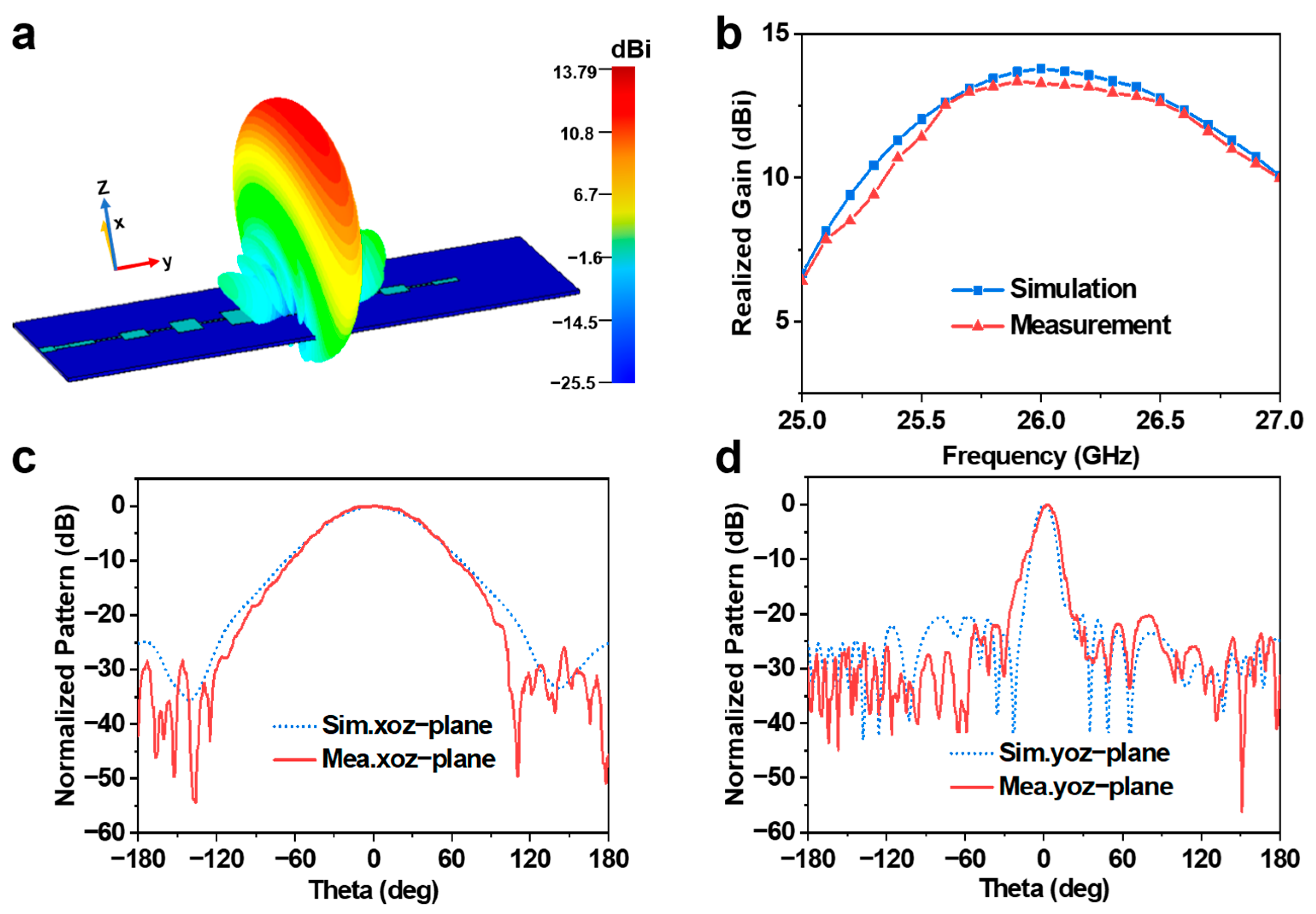
3.2. MXene Linear Array Antenna

Based on high-conductivity MXene film, a high gain planar array antenna (PAA) structure has been designed. The proposed MXene antenna comprises eight identical serially fed eight patches microstrip LAAs. The radiation patch consists of eight microstrip patches that satisfy the Chebyshev current distribution. The dielectric constant of the medium is assumed to be ε r ; the height is h; the operating frequency of antenna is f   a n d   Z c is the characteristic impedance of the microstrip feeding line which the width is W 0 . The physical dimensions of MXene based patches and microstrip lines are calculated by the following equations [30].
L = c 2   f r e s   ε reff   2 Δ L
W = c   2 2   f res ε r + 1
ε reff = ε r + 1 2 + ε r 1 2 1   + 12   h W 1 / 2
Δ L = 0.412   h   ε reff   +   0.3   W h   +   0.264 ε reff     0.258   W h   +   0.8
    Z c = 60 ε e   ln [ 8 h W 0 + W 0 4 h ] W 0 h     1 120   π ε e   [ W 0 h + 1.393 + 0.667   ln ( W 0 h + 1.444 ) ] W 0 h     1
In the equation, the physical length of the microstrip patch is L and the physical width of the microstrip patch is W. Rogers RT/durood 5880 PCB is the substrate ( ε r = 2.2, tan δ = 0.0009) with a thickness of 0.508 mm. The MXene array antenna was designed to operate at 25.5 GHz–26.5 GHz with a central frequency at 26 GHz. The structure is constructed and simulated in CST Studio. After the optimization of the parameters, the length of the patch unit is L = 3.9 mm and the width of central patches (W4 and W5) is 4.6 mm. The microstrip line with a characteristic impedance of 100 Ω has a width of W = 0.46 mm.
The sidelobe level of the uniform array antenna is relatively high, and the requirement of low sidelobes and high realized gain is hard to be reached in engineering applications. In order to satisfy the design requirements, the sidelobes levels are suppressed by the method of Chebyshev synthesis to achieve high gain. The distribution coefficients of current amplitude are calculated for each patch width using the method of Chebyshev synthesis as the following formula (The m-order Chebyshev polynomial T m is the solution of the second-order differential equation) [31].
  1 x 2   d 2 T m d x 2   x d T m dx + m 2   T m = 0
  T m x = c o s h mv = c o s h m   cos h 1 , x > 1 1 m c o s h mv = 1 m c o s h m   cos h 1   x , x < 1
The elements count of the MXene linear array are eight. The ratio of the normalized current amplitude of the MXene LAA’s each patch is obtained by the above equation. The radiated power ratio of each patch can be adjusted by controlling the width of each rectangular microstrip patch width to change the LAA array factor and radiation patterns of the MXene LAA. The radiation power ratio of each array can be guaranteed as long as the width of each patch meets the calculated current ratio. The patch width distribution of the LAA is presented as follows:
W1: W2: W3: W4: W5: W6: W7: W8 = 0.262: 0.519: 0.812: 1: 1: 0.812: 0.519: 0.262
Figure 3a shows the structure photograph of the serially fed MXene linear array antenna. A microstrip line feeds each patch in series along the y-axis direction. The input feeding port links with a section of 50 Ω microstrip line. For the purpose of matching the characteristic impedance between the feeding port and the adjacent patch [32], a quarter wavelength impedance converter is added, which can be seen from the red elliptical coils in Figure 3a. To ensure all patches have identical excitation phases, the distance between adjacent patches is approximately half of the equivalent wavelength of the operating frequency in the dielectric substrate with the feeding line impedance of 100 Ω. The structure of MXene array antenna is constructed and simulated in CST Studio. Figure 3b depicts the electric field distributions of LAA at 26 GHz. The maximum electric field amplitude is in two center patches of the LAA (W4, W5) and decreases sequentially along the two patches towards the sides, which conforms to Chebyshev distribution. To optimize antenna performance by dimensioning rectangular patches and microstrip transmission lines. The variables of the proposed MXene LAA after parametric optimizing are provided in Table 1. Figure 3c shows the digital photograph of MXene LAA produced by the method of laser engraving. VNA (Vector network analyzer, PNA-X N5247A of Agilent Technologies) is utilized to test the performance of MXene LAA, which coaxial connector selects 2.92 mm. Figure 3d describes the simulation and measurement of reflection coefficient results of MXene linear array antenna, the simulated resonant frequency is at 26 GHz and the simulated reflection coefficient is −35 dB. Compared with the simulation, the measured resonant frequency has a little frequency deviation. Human error in the production process causes the results. The bandwidth of the measured −10 dB impedance is 25.21–26.92 GHz with 188.8% of the simulation result.
To further research the radiation performance of LAA, the radiation properties of LAA were measured in a microwave anechoic chamber and compared to simulated data. Figure 4a depicts the three-dimensional (3D) radiation pattern of MXene LAA, the maximum radiation direction along the positive z-axis. The simulation and measurement of realized gain, normalized radiation patterns of LAA in the xoz-plane and yoz-plane are shown in Figure 4b–d. The peak realized gain in the bandwidth range of 25–27 GHz is 13.34 dBi which has a difference of 0.45 dBi compared with the simulation. The maximum difference in the direction of the main lobe between the simulated and measured is 3° approximately. The measured normalized radiation pattern values trend is similar to the simulation. The sidelobes levels (SLL) of yoz-plane is lower than −20 dB, which fulfills the design requirement. Compared to the xoz-plane radiation pattern, the half-power beam width of radiation pattern in yoz-plane is 12.4° which is a narrow beam, indicating the MXene LAA has a high angular resolution of detection in the yoz-plane. The results indicate MXene LAA has excellent performance at 25–26 GHz, which can be available for high gain array design.

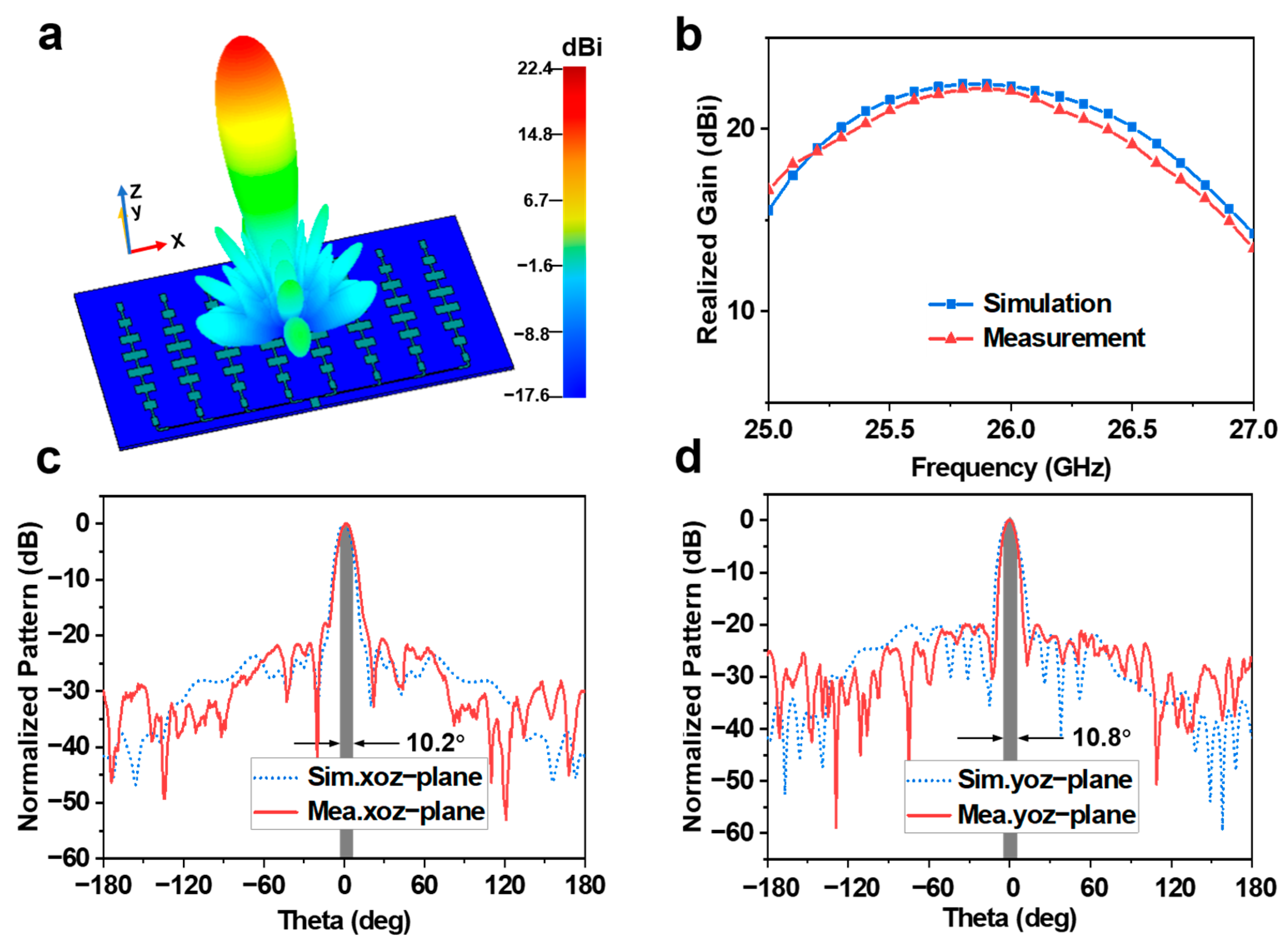
3.3. MXene High Gain Planar Array Antenna

The PAA consists of 8 identical LAAs connected by parallel feeding to obtain higher directionality and gain. Then, a one-input and eight-output feeding network is designed. The structure of the feeding network can be seen in Figure 5a which the feeding port is port 1 and the radiation ports are ports 2–9. In order to guarantee that each output port has the identical excitation phase, the spacing between the adjacent output port is λg (λg is the medium wavelength). To enable impedance matching of the feeding network, a quarter wavelength impedance converter (n1n4) is set in front of each output port which can be seen as symmetry about left and right.
Meanwhile, varying the widths of each quarter wavelength impedance converter to modify the characteristic impedance can control the power distribution between each output port. Table 1 demonstrates the optimized parameters. Figure 5b shows that each radiation port has the same phase at 26 GHz. The electric field distributions of the feeding network demonstrated in Figure 5c show that the electric field amplitude decays from the center to both sides, which conform to the design requirement. As well as the power of each radiation port is distributed to satisfy the Chebyshev distribution, which can be seen in Figure 5d.
After the feeding network meets the requirements, 8 identical LAAs are combined to form the MXene PAA. Figure 6a illustrates that the proposed MXene PAA with the geometrical dimensions of 75 mm × 75 mm is fabricated by the method of laser engraving. The radiation state of the array antenna can be observed through the distribution of the surface electric field. Figure 6b demonstrates the electric field distribution of MXene PAA, which demonstrates central symmetry. The electric field amplitude is the strongest at the center feeding port and weakens gradually at the edge, which complies with the Chebyshev current distribution. Figure 6c describes the measurement’s reflection coefficient results of MXene PAA, the resonant frequency is at 26 GHz and the reflection coefficient is −31.8 dB. The impendence bandwidth of the PAA is less than −10 dB in the range of 24–28 GHz, which demonstrates the MXene PAA has broadband performance and covers the frequency band of 5G FR2—n258. The lower Q value of MXene PAA results in wideband characteristic benefits.
Figure 7a depicts the three-dimensional (3D) radiation pattern of MXene PAA and the maximum radiation direction is along the positive z-axis. Figure 7b illustrates the simulation and measurement of realized gain of the PAA. The peak value reaches 22.22 dBi, which only has a loss of 0.24 dBi compared with the simulation result, which is permissible in the design of array antenna. As displayed in Figure 7c,d, the normalized patterns of MXene PAA in the xoz-plane and yoz-plane are similarly measured in the anechoic chamber. The half power beam width of MXene PAA in the xoz-plane and yoz-plane are 10.2° and 10.8°, respectively. Compared with the LAA radiation beam are narrower. Simulation and measurement of normalized patterns have the same half-power beam width and similar trends. The sidelobes levels of the xoz-plane and yoz-plane are below −20 dB, which matches the design aim.

4. Conclusions

In conclusion, it is the first attempt to manufacture the MXene millimeter wave band antenna with promising performance. The proposed millimeter wave array antenna made of high-conductivity MXene film has the advanced properties of wideband, low sidelobes and high gain. The results of measurement are in excellent correspondence with the simulated. The MXene PAA with Chebyshev distribution operates at 26 GHz with the −10 dB impedance bandwidth of measurement from 24 GHz to 28 GHz, which satisfies the 5G MMW communication band. The peak realized gain reaches up to 22.22 dBi. The sidelobes of MXene PAA radiation patterns are lower than −20 dB and have a narrow half-power beam width of 10.2° and 10.8° in the xoz-plane and yoz-plane radiation patterns, respectively. We are convinced there is still considerable space for performance enhancement. The MXene PAA shows enormous potential for MMW applications in diverse fields like IoTs, healthcare, radar, 5G communication, etc.

Author Contributions

Conceptualization, H.Z. and Y.S.; methodology, R.S., B.-W.L. and D.H.; software, J.G.; validation, D.Y., M.X., H.Z., Y.S. and Y.X.; investigation, J.G. and R.S.; writing—original draft preparation, J.G., R.S. and Y.S.; supervision, D.H. and B.-W.L.; funding acquisition, D.H. All authors have read and agreed to the published version of the manuscript.

Funding

This research was funded by the National Natural Science Foundation of China Grant No. 51672204, 51701146, 62001338, the Fundamental Research Funds for the Central Universities No. WUT: 2020IB005, 205209016 and 2019IB017.

Institutional Review Board Statement

Not applicable.

Informed Consent Statement

Not applicable.

Data Availability Statement

Data are available from authors upon request.

Conflicts of Interest

The authors declare no conflict of interest.

References

  1. Jia, Q.; Xu, H.; Xiong, M.F.; Zhang, B.; Duan, J. Omnidirectional Solid Angle Beam-Switching Flexible Array Antenna in Millimeter Wave for 5G Micro Base Station Applications. IEEE Access 2019, 7, 157027–157036. [Google Scholar] [CrossRef]
  2. Uwaechia, A.N.; Mahyuddin, N.M. A Comprehensive Survey on Millimeter Wave Communications for Fifth-Generation Wireless Networks: Feasibility and Challenges. IEEE Access 2020, 8, 62367–62414. [Google Scholar] [CrossRef]
  3. Jijo, B.T.; Zeebaree, S.R.M.; Zebari, R.R.; Sadeeq, M.A.M.; Sallow, A.B.; Mohsin, S.; Ageed, Z.S. A Comprehensive Survey of 5G mm-Wave Technology Design Challenges. Asian J. Res. Comput. Sci. 2021, 8, 1–20. [Google Scholar] [CrossRef]
  4. Hong, W.; Jiang, Z.H.; Yu, C.; Zhou, J.; Chen, P.; Yu, Z.; Zhang, H.; Yang, B.; Pang, X.; Jiang, M.; et al. Multibeam Antenna Technologies for 5G Wireless Communications. IEEE Trans. Antenn. Propag. 2017, 65, 6231–6249. [Google Scholar] [CrossRef]
  5. Semkin, V.; Ferrero, F.; Bisognin, A.; Ala-Laurinaho, J.; Luxey, C.; Devillers, F.; Räisänen, A.V. Beam switching conformal antenna array for mm-wave communications. IEEE Antenn. Wirel. Propag. Lett. 2015, 15, 28–31. [Google Scholar] [CrossRef]
  6. Ohlen, P.; Skubic, B.; Rostami, A.; Fiorani, M.; Monti, P.; Ghebretensae, Z.; Martensson, J.; Wang, K.; Wosinska, L. Data Plane and Control Architectures for 5G Transport Networks. J. Light. Technol. 2016, 34, 1501–1508. [Google Scholar] [CrossRef]
  7. Ur-Rehman, M.; Abbasi, Q.H.; Rahman, A.; Khan, I.; Chattha, H.T.; Matin, M.A. Millimetre-Wave Antennas and Systems for the Future 5G. Int. J. Antenn. Propag. 2017, 2017, 6135601. [Google Scholar] [CrossRef]
  8. Mao, C.; Khalily, M.; Xiao, P.; Brown, T.W.C.; Gao, S. Planar Sub-Millimeter-Wave Array Antenna with Enhanced Gain and Reduced Sidelobes for 5G Broadcast Applications. IEEE Trans. Antenn. Propag. 2019, 67, 160–168. [Google Scholar] [CrossRef] [Green Version]
  9. Jilani, S.F.; Munoz, M.O.; Abbasi, Q.H.; Alomainy, A. Millimeter-Wave Liquid Crystal Polymer Based Conformal Antenna Array for 5G Applications. IEEE Antenn. Wirel. Propag. Lett. 2019, 18, 84–88. [Google Scholar] [CrossRef] [Green Version]
  10. Jiang, S.; Song, R.; Hu, Z.; Xin, Y.; Huang, G.L.; He, D. Millimeter wave phased array antenna based on highly conductive graphene-assembled film for 5G applications. Carbon 2022, 196, 493–498. [Google Scholar] [CrossRef]
  11. Song, R.; Wang, Z.; Zu, H.; Chen, Q.; Mao, B.; Wu, Z.P.; He, D. Wideband and low sidelobe graphene antenna array for 5G applications. Sci. Bull. 2021, 66, 103–106. [Google Scholar] [CrossRef]
  12. Song, R.; Mao, B.; Wang, Z.; Hui, Y.; Zhang, Z.; Fang, R.; Zhang, J.; Wu, Y.; Ge, Q.; Novoselov, K.S.; et al. Comparison of copper and graphene-assembled films in 5G wireless communication and THz electromagnetic-interference shielding. Proc. Natl. Acad. Sci. USA 2023, 120, e2085160176. [Google Scholar] [CrossRef]
  13. Rutherglen, C.; Jain, D.; Burke, P. Nanotube electronics for radiofrequency applications. Nat. Nanotechnol. 2009, 4, 811–819. [Google Scholar] [CrossRef] [PubMed]
  14. Zhang, H.B.; Zheng, W.G.; Yan, Q.; Jiang, Z.G.; Yu, Z.Z. The effect of surface chemistry of graphene on rheological and electrical properties of polymethylmethacrylate composites. Carbon 2012, 50, 5117–5125. [Google Scholar] [CrossRef]
  15. Shen, B.; Zhai, W.T.; Zheng, W.G. Ultrathin Flexible Graphene Film: An Excellent Thermal Conducting Material with Efficient EMI Shielding. Adv. Funct. Mater. 2014, 24, 4542–4548. [Google Scholar] [CrossRef]
  16. Zhang, J.Z.; Kong, N.; Uzun, S.; Levitt, A.; Seyedin, S.; Lynch, P.A.; Qin, S.; Han, M.K.; Yang, W.R.; Liu, J.Q.; et al. Scalable Manufacturing of Free-Standing, Strong Ti3C2Tx MXene Films with Outstanding Conductivity. Adv. Mater. 2020, 32, 2001093. [Google Scholar] [CrossRef] [PubMed]
  17. Jiang, J.; Bai, S.; Zou, J.; Liu, S.; Hsu, J.; Li, N.; Zhu, G.; Zhuang, Z.; Kang, Q.; Zhang, Y. Improving stability of MXenes. Nano Res. 2022, 15, 6551–6567. [Google Scholar] [CrossRef]
  18. VahidMohammadi, A.; Rosen, J.; Gogotsi, Y. The world of two-dimensional carbides and nitrides (MXenes). Science 2021, 372, eabf1581. [Google Scholar] [CrossRef]
  19. Naguib, M.; Kurtoglu, M.; Presser, V.; Lu, J.; Niu, J.J.; Heon, M.; Hultman, L.; Gogotsi, Y.; Barsoum, M.W. Two-Dimensional Nanocrystals Produced by Exfoliation of Ti3AlC2. Adv. Mater. 2011, 23, 4248–4253. [Google Scholar] [CrossRef] [Green Version]
  20. Zhang, H.; Wang, L.; Chen, Q.; Li, P.; Zhou, A.; Cao, X.; Hu, Q. Preparation, mechanical and anti-friction performance of MXene/polymer composites. Mater. Des. 2016, 92, 682–689. [Google Scholar] [CrossRef]
  21. Han, M.K.; Shuck, C.E.; Rakhmanov, R.; Parchment, D.; Anasori, B.; Koo, C.M.; Friedman, G.; Gogotsi, Y. Beyond Ti3C2Tx: MXenes for Electromagnetic Interference Shielding. ACS Nano 2020, 14, 5008–5016. [Google Scholar] [CrossRef]
  22. Sarycheva, A.; Polemi, A.; Liu, Y.L.; Dandekar, K.; Anasori, B.; Gogotsi, Y. 2D titanium carbide (MXene) for wireless communication. Sci. Adv. 2018, 4, eaau0920. [Google Scholar] [CrossRef] [PubMed] [Green Version]
  23. Li, Y.; Tian, X.; Gao, S.P.; Jing, L.; Li, K.; Yang, H.; Fu, F.; Lee, J.Y.; Guo, Y.X.; Ho, J.S.; et al. Reversible Crumpling of 2D Titanium Carbide (MXene) Nanocoatings for Stretchable Electromagnetic Shielding and Wearable Wireless Communication. Adv. Funct. Mater. 2019, 30, 1907451. [Google Scholar] [CrossRef]
  24. Han, M.; Liu, Y.; Rakhmanov, R.; Israel, C.; Tajin, M.A.S.; Friedman, G.; Volman, V.; Hoorfar, A.; Dandekar, K.R.; Gogotsi, Y. Solution-Processed Ti3C2Tx MXene Antennas for Radio-Frequency Communication. Adv. Mater. 2021, 33, 2003225. [Google Scholar] [CrossRef] [PubMed]
  25. Zhao, W.; Ni, H.; Ding, C.; Liu, L.; Fu, Q.; Lin, F.; Tian, F.; Yang, P.; Liu, S.; He, W.; et al. 2D Titanium carbide printed flexible ultrawideband monopole antenna for wireless communications. Nat. Commun. 2023, 14, 278. [Google Scholar] [CrossRef]
  26. Shao, Y.; Wei, L.; Wu, X.; Jiang, C.; Yao, Y.; Peng, B.; Chen, H.; Huangfu, J.; Ying, Y.; Zhang, C.J.; et al. Room-temperature high-precision printing of flexible wireless electronics based on MXene inks. Nat. Commun. 2022, 13, 3223. [Google Scholar] [CrossRef]
  27. Si, Y.; Jin, H.; Zhang, Q.; Xu, D.; Xu, R.; Ding, A.; Liu, D. Roll-to-roll processable MXene-rGO-PVA composite films with enhanced mechanical properties and environmental stability for electromagnetic interference shielding. Ceram. Int. 2022, 48, 24898–24905. [Google Scholar] [CrossRef]
  28. Fang, X.-Y.; Yu, X.-X.; Zheng, H.-M.; Jin, H.-B.; Wang, L.; Cao, M.-S. Temperature- and thickness-dependent electrical conductivity of few-layer graphene and graphene nanosheets. Phys. Lett. A 2015, 379, 2245–2251. [Google Scholar] [CrossRef]
  29. Song, R.; Zhao, X.; Wang, Z.; Fu, H.; Han, K.; Qian, W.; Wang, S.; Shen, J.; Mao, B.; He, D. Sandwiched Graphene Clad Laminate: A Binder-Free Flexible Printed Circuit Board for 5G Antenna Application. Adv. Eng. Mater. 2020, 22, 2000451. [Google Scholar] [CrossRef]
  30. Song, R.; Huang, G.L.; Liu, C.; Zhang, N.; Zhang, J.; Liu, C.; He, D. High-conductive graphene film based antenna array for 5G mobile communications. Int. J. RF Microw. Comput. Aided Eng. 2019, 29, e21692. [Google Scholar] [CrossRef]
  31. Barbiere, D. A method for calculating the current distribution of Tschebyscheff arrays. Proc. IRE 1952, 40, 78–82. [Google Scholar] [CrossRef]
  32. Guo, Y.Q.; Pan, Y.M.; Zheng, S.Y. Design of Series-Fed, Single-Layer, and Wideband Millimeter-Wave Microstrip Arrays. IEEE Trans. Antenn. Propag. 2020, 68, 7017–7026. [Google Scholar] [CrossRef]
Figure 1. (a) The preparation process diagram of the MXene array antenna. (b) Digital photograph of MXene film. (c) XRD patterns of Ti3C2 flakes and Ti3AlC2 MAX phase. (d) Raman spectrum of MXene film.
Crystals 13 01136 g001
Figure 2. (a) TEM image of MXene Nanosheet. (b) Top-view SEM image of MXene film. (c) Cross-sectional SEM image of MXene film. (d) A typical laminar structure SEM image of the MXene film cross-section.
Crystals 13 01136 g002
Figure 3. (a) Structure photograph of MXene LAA. (b) Electric field distributions of LAA at 26 GHz. (c) Digital photograph of MXene LAA. (d) Simulated and measured reflection coefficient of MXene LAA.
Crystals 13 01136 g003
Figure 4. (a) Three-dimensional radiation pattern of MXene LAA. (b) Simulated and measured realized gain of MXene LAA. (c) Simulated and measured xoz-plane normalized patterns of MXene LAA. (d) Simulated and measured yoz-plane normalized patterns of MXene LAA.
Crystals 13 01136 g004
Figure 5. (a) Structure photograph of the feeding network of PAA. (b) Phase distribution of output ports in the feeding network. (c) Electric field distributions of feeding network of PAA at 26 GHz. (d) S-parameter of output ports in the feeding network.
Crystals 13 01136 g005
Figure 6. (a) Digital photograph of MXene PAA. (b) Electric field distributions of MXene PAA at 26 GHz. (c) Measured reflection coefficient of MXene PAA.
Crystals 13 01136 g006
Figure 7. (a) Three-dimensional radiation pattern of MXene PAA. (b) Simulated and measured realized gain of MXene PAA. (c) Simulated and measured xoz-plane normalized patterns of MXene PAA. (d) Simulated and measured yoz-plane normalized patterns of MXene PAA.
Crystals 13 01136 g007
Table 1. Geometric parameters of the proposed MXene array antenna.
ParameterLWW1W2W3W4W5W6
Value (mm)3.90.461.212.393.744.64.63.74
ParameterW7W8W0W50n1n2n3n4
Value (mm)2.391.2111.6110.670.971.16
Disclaimer/Publisher’s Note: The statements, opinions and data contained in all publications are solely those of the individual author(s) and contributor(s) and not of MDPI and/or the editor(s). MDPI and/or the editor(s) disclaim responsibility for any injury to people or property resulting from any ideas, methods, instructions or products referred to in the content.

