Article

Performance Comparison of SONOS-Type UV TD Sensor Using Indium Tin Oxide-Aluminum Oxide-Zirconia Aluminum Oxide-Silicon Oxide-Silicon and Indium Tin Oxide-Aluminum Oxide-Hafnium Aluminum Oxide-Silicon Oxide-Silicon

1
Electronic Engineering Department, Southern Taiwan University of Science and Technology, Nan-Tai Street, Yungkang District, Tainan 71005, Taiwan
2
Opto-Electronic System Engineering Department, Minghsin University of Science and Technology, Xinfeng 30401, Taiwan
*
Authors to whom correspondence should be addressed.
Crystals 2023, 13(7), 1092; https://doi.org/10.3390/cryst13071092
Submission received: 31 May 2023 / Revised: 9 July 2023 / Accepted: 10 July 2023 / Published: 13 July 2023
(This article belongs to the Special Issue Optoelectronics and Photonics in Crystals)

Abstract

:
This study compares the performance of two types of capacitive devices, indium tin oxide-aluminum oxide-zirconia aluminum oxide-silicon oxide-silicon (IAZAOS) and indium tin oxide-aluminum oxide-hafnium aluminum oxide-silicon oxide-silicon (IAHAOS), as silicon-oxide-nitride-oxide-silicon (SONOS) non-volatile memory (NVM) total dose of ultraviolet radiation (UV TD) sensors. Results show that IAZAOS with zirconia aluminum oxide as the charge-trapping layer outperforms IAHAOS with hafnium aluminum oxide for a UV TD sensor. After exposure to UV TD irradiation of 100 mW·s/cm2, the threshold voltage (VT) change of IAZAOS is almost 1.25 times that of IAHAOS. The study also found that annealing can significantly improve the response performance of IAZAOS UV TD sensors. Furthermore, IAZAOS devices with partially smaller nanocrystals in the charge-trapping layer greatly enhance the response of SONOS-type UV TD sensors. The study also compared the constant voltage stress-induced leakage current (CVSILC) and found that the CVSILC for annealed IAZAOS devices is 1000 times smaller than that of IAHAOS devices. Moreover, the IAZAOS-I2Z2 exhibits a superior performance regarding irradiation/refresh cycle endurance as compared to the IAHAOS-I2H1 device. These findings suggest that IAZAOS capacitive devices have superior performance and potential for use in SONOS-type UV TD sensors.

1. Introduction

Keeping track of the total dose of ultraviolet radiation (UV TD) is of utmost importance as it can have severe health implications such as skin cancer, cataracts, and immune system suppression. UV TD is the cumulative amount of UV radiation that a person is exposed to over a specific period. UV radiation finds its application in various fields, including safety, medicine, defense, and industry [1,2]. Therefore, monitoring UV TD can aid in developing effective preventive measures and public health policies. Different methods are available to measure UV TD, including personal dosimeters, ground-based monitoring stations, and satellite-based measurements. Accurate monitoring of UV TD can help in reducing the potential risk of harmful health effects associated with excessive UV exposure [1,2].

1.1. Six Types Semiconductor Based Radiation Sensors

(1)
Silicon diode: reverse biased p-n junction;
(2)
Silicon PIN: p-type–intrinsic–n-type diode;
(3)
RADFET: radiation-sensitive field-effect transistor;
(4)
FOXFET: field-oxide field-effect transistor;
(5)
FGMOS: floating gate metal-oxide-semiconductor field-effect transistors;
(6)
SONOS: silicon-silicon oxide-silicon nitride-silicon oxide-silicon non-volatile memory.
In the case of silicon diode and silicon PIN diode-type sensors, a higher bias is applied, and a smaller current is measured. Therefore, the diode should have a larger size to increase the sensitivity of the diode and PIN-type sensors. Sensor shrinkage is very important for advanced nanoscale standard CMOS semiconductor process-compatible applications.
For RADFET and FOXFET FET-type sensors, the charge generated by radiation is unstable. When the sensors’ data are read, the charge generated by the radiation will be released. Silicon diodes, silicon PIN diodes, RADFETs, and FOXFETs are commonly used for high-dose level measurement applications. Silicon diode, silicon PIN, RADFET, and FOXFET sensors are not non-volatile memory (NVM), so the data will be volatile [3,4,5].
Dosimeters based on FGMOS technology exhibit high sensitivity to radiation doses, which results in sensor responses becoming saturated at low dose levels. As a result, these sensors are typically only suitable for measuring low levels of radiation. While FGMOS is a type of non-volatile memory (NVM), it has drawbacks such as poor endurance, data retention, and slow program/erase speed when compared to SONOS-type NVM [3,4,5].
Six types of semiconductor-based radiation sensors were compared, as shown in Table 1 [6,7,8,9,10].

1.2. SONOS NVM–Type UV TD Sensor

Research of Non-Volatile Memory (NVM) devices has been driven by the limitations of Floating Gate (FG) storage devices in terms of reducing device size and simplifying manufacturing processes. One promising candidate for the next generation of NVM devices is the Silicon-Oxide-Nitride-Oxide-Silicon (SONOS) device, which has been shown to scale down to the nanoscale and possesses coupling-free and MOS-like structures. Previous studies have demonstrated that a SONOS-like NVM device could be used as a non-volatile UV TD sensor, as the UV-generated charges can be permanently captured inside the trapping layer of the SONOS NVM device [11,12]. An external circuit can then detect changes in the amount of trapped charge inside the SONOS NVM trapping layer after UV exposure. However, Next-generation NVM devices are expected to use high-k gate dielectric materials in silicon-oxide-hafnium oxide-silicon-oxide-silicon SOHOS-like structures, as they have shown better scalability and performance compared to the SONOS structure. One such device, the Poly Silicon-Aluminum Oxide-Hafnium Aluminum Oxide-Silicon Oxide-Silicon (hereafter SAHAOS) with a high k gate dielectric, has been demonstrated to perform better as an NVM UV TD sensor than a SONOS sensor [13,14,15,16,17]. Moreover, an indium tin oxide-silicon oxide-hafnium aluminum oxide-silicon oxide-silicon (hereafter IOHAOS) device with UV transparency indium tin oxide ITO gate has been found to greatly increase the response of a SONOS-type UV TD sensor and has been shown to perform better than a SAHAOS with poly silicon gate device. Compared to other semiconductor-based radiation sensors, IOHAOS NVM UV TD sensors offer several advantages, including high sensitivity, small size, data dependence on UV TD, non-volatile data storage, erasable data, use of high-k semiconductor technology, simple data reading equipment, and tunable sensitivity, as demonstrated by previous studies [18,19,20].
This study showcases the effectiveness of an indium tin oxide-aluminum oxide-zirconia aluminum oxide-silicon oxide-silicon capacitor device with zirconia aluminum oxide as the charge-trapping layer (hereafter IAZAOS) in significantly enhancing the response of a SONOS-type UV TD sensor. The paper proposes a novel material, ZrAlOx, which differs from the HfAlOx material discussed in a prior publication [20]. However, unlike the previous fabrication process, the ZrAlOx and HfAlOx materials in this paper were produced using an ALD machine. The research highlights that the use of an IAZAOS device with zirconia aluminum oxide as the charge-trapping layer performs better as a non-volatile memory (NVM) UV TD sensor compared to an IAHAOS device with hafnium aluminum oxide as the charge-trapping layer. The study compares the UV-induced threshold voltage VT changes for various IAZAOS capacitor devices with different annealing temperatures for IAZAOS. The research reveals that the UV TD sensing response of an IAZAOS UV TD sensor is significantly improved by annealing for IAZAOS. Lastly, the research compares the constant voltage stress-induced leakage current (CVSILC) and finds that the CVSILC for the IAZAOS device was significantly better than that of the IAHAOS device. Moreover, the performance of the IAZAOS-I2Z2 device was better than the IAHAOS-I2H1 device in terms of irradiation/refresh cycle characteristics.

2. Materials and Methods

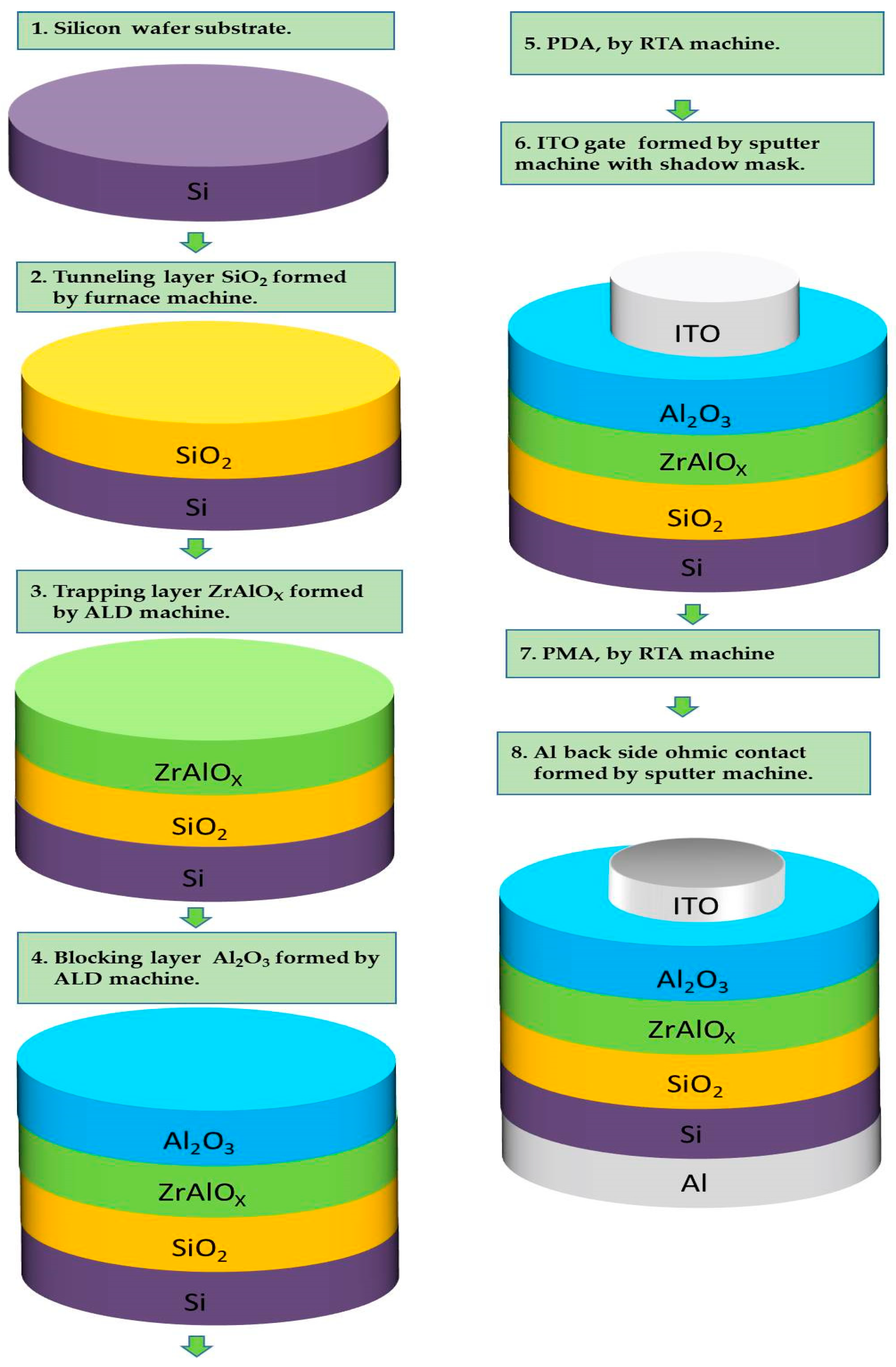
2.1. Sensor Manufacturing Details

Eight manufacturing steps for the IAZAOS/IAHAOS UV TD sensor capacitor were used in the study:
(1)
Substrate: we used p-type Si <100> substrate with a resistivity of 15–25 ohm-cm as substrate;
(2)
Tunneling oxide: we used silicon oxide SiO2 (3~5 nm) as tunneling oxide thermally grown by an advanced clustered vertical furnace (ASMA-400) at 925 °C;
(3)
Trapping oxide: we used zirconia aluminum oxide ZrAlOx or hafnium aluminum oxide HfAlOx films (10~30 nm) with 10~40% Al as composition ratio as trapping oxide deposited by Atomic Layer Chemical Vapor Deposition System, ALD (Cambridge NanoTech Fiji-202 DCS, Cambridge, MA, USA);
(4)
Blocking oxide: we used aluminum oxide Al2O3 (10~20 nm) as blocking oxide by ALD System (Cambridge NanoTech Fiji-202 DCS, Cambridge, USA);
(5)
PDA: we process post-dielectric annealing (PDA) at different temperatures by a rapid thermal annealing (RTA) (ALLWIN21 AccuThermo AW 810 M, Morgan Hill, USA);
(6)
Gate electrode: we use the indium tin oxide ITO (200–400 nm) as gate electrode deposited by sputter machine (Fulintec-FSE, Tainan, Taiwan). ITO ceramics target with 90% (wt. ratio) In2O3 and 10% (wt. ratio) SnO2 is used;
(7)
PMA: we process post-gate conductor annealing (PMA) at different temperatures by a rapid thermal annealing (RTA) (ALLWIN21 AccuThermo AW 810 M, Morgan Hill, USA) process
(8)
Substrate back side ohmic contact: we used Aluminum Al (200~400 nm) sputtered by sputter machine (Fulintec-FSE, Tainan, Taiwan).
The top view optical microscope OM image of the IAZAOS UV TD sensor is shown in Figure 1. In Figure 2, the 3D fabrication process flow of the IAZAOS capacitor UV TD sensor is shown. The article introduces a novel material called ZrAlOx, which distinguishes itself from the previously used HfAlOx material discussed in a previous article [20]. However, unlike the previous article, where the HfAlOx material was produced using MOCVD, the HfAlOx material in this article was made using an ALD machine. The article introduces a novel material ZrAlOx, which distinguishes itself from the previously used HfAlOx material discussed in a previous article [20]. However, unlike the previous article, where the HfAlOx material was produced using MOCVD, the HfAlOx material in this article was made using an ALD machine.
In the ALD system, trimethylaluminum (TMA) Al₂(CH₃)₆, Tetrakis(dimethylamino)hafnium (TEMAH) Hf[N(CH3)(C2H5)] 4, Tetrakis(dimethylamino)zirconium (TEMAZ) Zr[N (CH3)(C2H5)]4 were used as the Hf, Zr, and Al precursors, respectively.
To compare the UV TD sensor performance for IAZAOS/IAHAOS devices with different PDA and PMA temperatures, six types of IAZAOS/IAHAOS with different PDA and PMA temperatures were fabricated, as shown in Table 2.
In this study, these IAZAOS/IAHAOS capacitor devices with different PDA and PMA have the same thickness of the tunneling oxide, trapping oxide, blocking oxide layer, and control gate layer for the IAZAOS/IAHAOS UV TD sensor performance comparison.

2.2. UV TD Sensor Operation Measurement

In this study, three procedures are employed for operating the SONOS-like NVM UV TD sensor. Firstly, the data writing procedure applies both UV and a positive gate voltage (PGV) to the sensor, using UV radiation sources with wavelengths of 405 nm, 375 nm, 350 nm, and 325 nm. The UV TD sensor data writing is performed with a PGV ranging from 5 to 25 volts. Secondly, the data read procedure utilizes the HP4284 CG–VG meter to measure changes in the CG–VG curve after UV TD exposure. Finally, the data erase procedure involves injecting positive charges under a negative gate voltage (NGV) to erase the UV TD data in the SONOS-like NVM UV TD sensor, restoring it to its original pre-irradiated refresh state.
Table 3 lists various UV TD, PGV, and UV wavelength conditions for the IAZAOS NVM UV TD sensor. This article compares the responses to four different UV wavelengths, which is different from previous studies.

2.3. Sensor Material Analysis

There are four methods for sensor material inspection in this study:
(1)
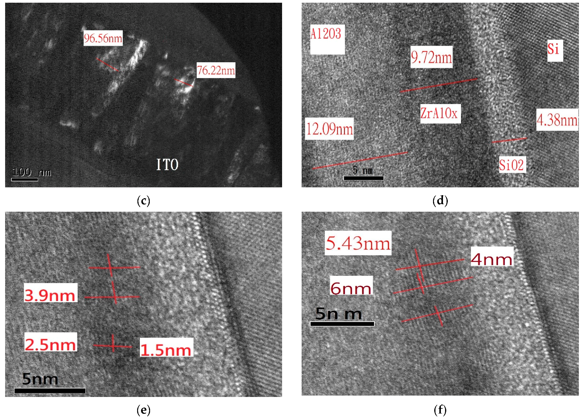
TEM: transmission electron microscopy (TEM) (JEOL JEM-2010F, Tokyo, Japan) was used for crystallization analysis of IAZAOS with various PDA and PMA temperature conditions;
(2)
XRD: X-ray diffraction analysis (XRD) (PANalytical X’Pert Pro, Westborough, MA, USA) was used for crystallization analysis of the various IAZAOS with various PMA temperature conditions;
(3)
Optical spectrometer: optical transmission spectroscopy analysis machine (Shimadzu-UV-250, Kyoto, Japan) was used for optical transmission analysis of various IAZAOS control gate films material prepared with various post-anneal temperature conditions;
(4)
OM: optical microscope analysis machine (Olympus-BX63, Tokyo, Japan) was used for top view image of IAZAOS capacitor device.

3. Results

3.1. UV-Induced VT Shift in IAZAOS

Figure 3 displays the frequency-dependent CG–VG responses of the IAZAOS-I2Z2 and IAHAOS-I2H1 devices in their virgin state, covering the range of 1 kHz to 100 kHz. While the inversion responses are similar in both cases, the IAZAOS device shows greater dispersion in the accumulation region compared to the IAHAOS device. In addition, the IAZAOS device also exhibited higher cumulative capacitance compared to the IAHAOS device.
In Figure 4, the CG–VG curve of an IAZAOS-I2Z2 capacitor device is shown before and after exposure to W405UV100G15 irradiation. The CG–VG curve was measured at a frequency of 100 kHz. The device was erased using NGV −15V before UV irradiation. The solid line represents the CG–VG curve before exposure to UV, while the dashed line represents the CG–VG curve after exposure to UV TD up to 100 mW·s/cm2. It is evident that the CG–VG curve shifted to the right after exposure to UV TD, indicating a positive shift in VT. This positive shift in VT is consistent with previous research studies [18,20]
Figure 5a–d illustrate the correlation between the increase in UV-induced VT and the UV TD for an IAZAOS sensor under 405 nm, 375 nm, 350 nm, and 325 nm wavelength UV radiation, respectively. Previous studies [18,20] were also referenced. The results in Figure 5 show that the IAZAOS-I2Z2 capacitor exhibited a VT increase of approximately 9.2 V, 8.8 V, 8 V, and 6.5 V after exposure to W405UV100G15, W375UV100G15, W350UV100G15, and W325UV100G15 irradiation conditions, respectively.

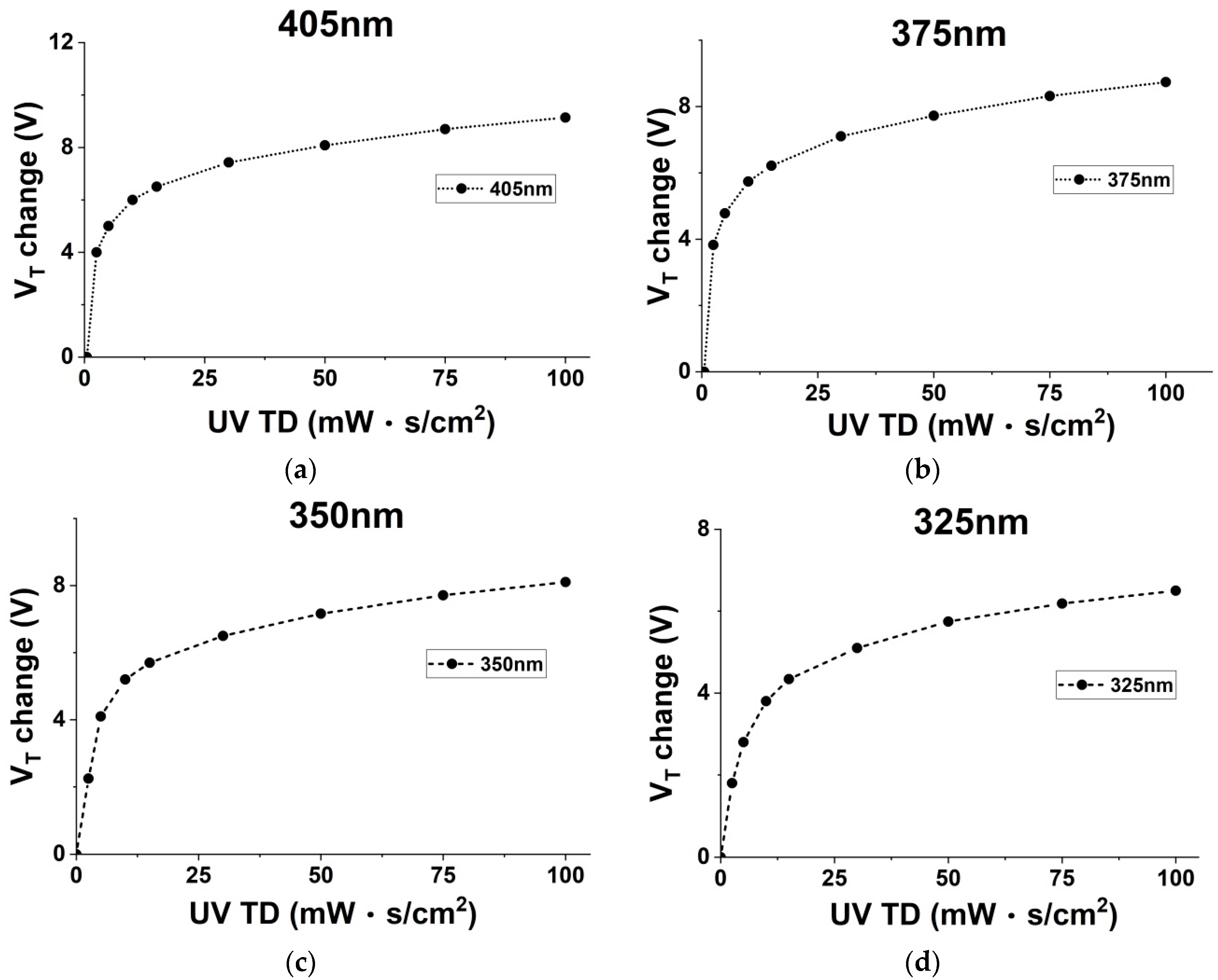
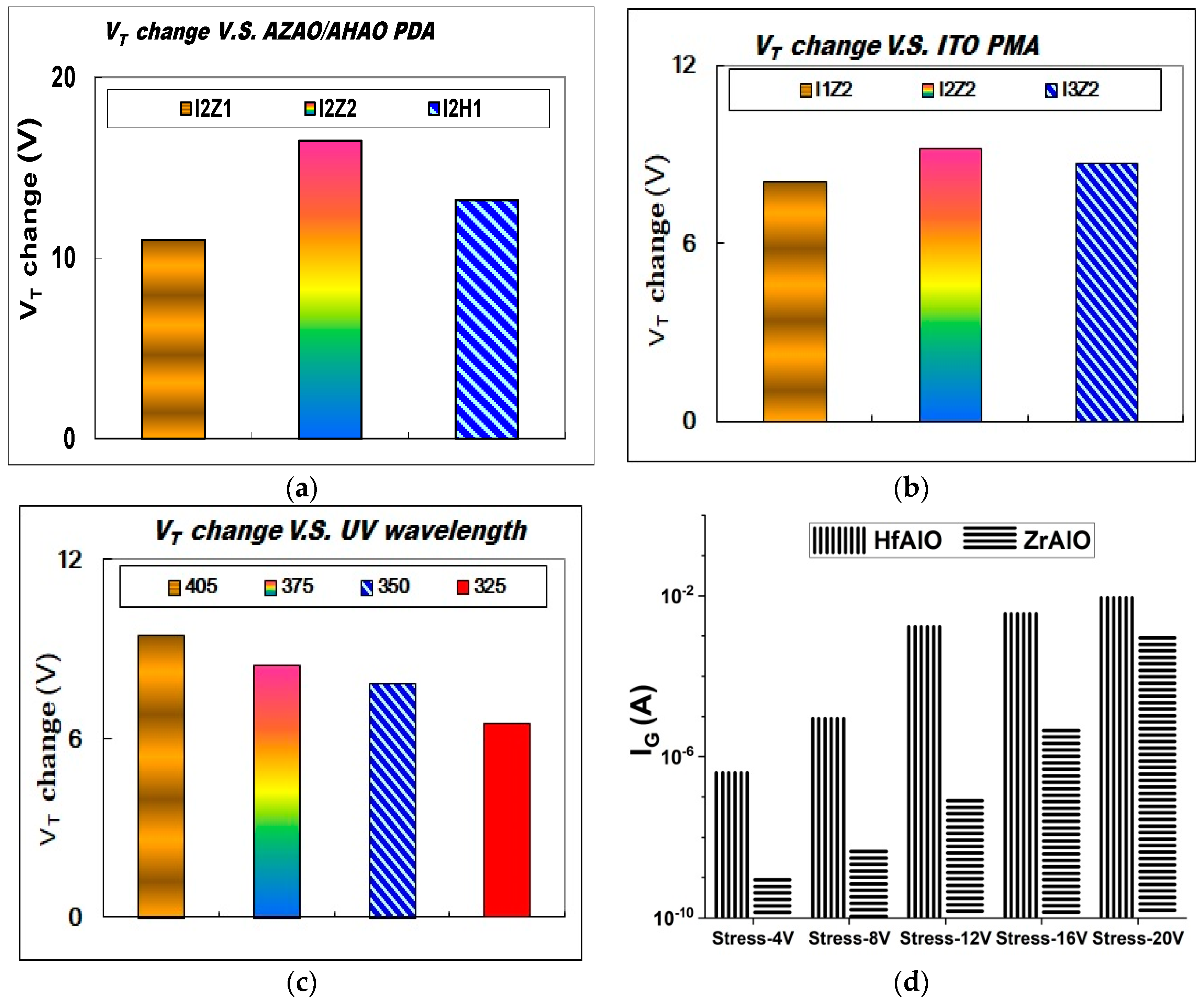
3.2. UV-Induced VT Change Comparison for Various IAZAOS at Different UV Wavelengths and Different Annealing Temperatures

In Figure 6a, a comparison of the UV-induced VT change is presented for various IAZAOS capacitor devices with different PDA anneal temperatures after exposure to W405U100G15 irradiation conditions. The results show that the IAZAOS-I2Z2 capacitor device with 1000 °C 30 s PDA exhibited a VT change almost 1.5 times greater than that of the IAZAOS-I2Z1 device with 900 °C 30 s PDA under W405UV100G25 irradiation condition. Furthermore, it was found that the VT change of the IAHAOS-I2H1 device was smaller than that of the IAZAOS-I2Z2 device under the same irradiation condition. As shown in Figure 6a, the UV-induced VT change for the IAZAOS-I2Z2 device with 1000 °C 30 s PDA was almost 1.25 times greater than that of the IAHAOS-I2H1 device with the same PDA anneal condition under W405UV100G25. Overall, the IAZAOS-I2Z2 device exhibited a greater VT change after UV irradiation compared to the IAHAOS-I2H1 and IAZAOS-I2Z1 devices.
Figure 6 b displays a comparison of the UV-generated VT change for various IAZAOS capacitor devices with different ITO PMA temperatures after exposure to the W405U100G15 irradiation condition. The results indicate that the VT change of the IAZAOS-I2Z2 device was most significant compared to the IAZAOS-I1Z2 and IAZAOS-I3Z2 devices under the same irradiation condition. Specifically, as shown in Figure 6b, the VT change of the IAZAOS-I2Z2 device with 500 °C 30 s ITO PMA was almost 1.1 times greater than that of the IAZAOS-I1Z2 device with 250 °C 30 s ITO PMA.
In Figure 6c, a comparison of the UV-generated change is presented for IAZAOS-I2Z2 devices after UV100 irradiation with different UV wavelengths. The results show that the VT change of the IAZAOS-I1Z2 device under the 405 nm UV irradiation condition was most significant compared to the 375 nm, 350 nm, and 325 nm UV irradiation conditions, as shown in Figure 6c. Specifically, the VT change of the IAZAOS-I2Z2 device with W405UV100G15 irradiation was almost 1.1 times greater than that with W375UV100G15 irradiation, almost 1.3 times greater than that with W350UV100G15 irradiation, and almost 1.5 times greater than that with W325UV100G15 irradiation. It is worth noting that even under the W325UV100G15 condition, the VT change of the IAZAOS-I2Z2 device was still almost as high as 6 volts, as depicted in Figure 6c.
In Figure 6d, a comparison of the CVSILC for IAZAOS and IAHAOS devices is presented. The results show that the CVSILC of the IAHAOS-I2H1 device was almost 1000 times greater than that of the IAZAOS-I2Z2 under −12 V VG pressure for 100 s, as depicted in Figure 6d. Specifically, the CVSILC of the IAHAOS-I2H1 device under −12 V VG pressure for 100 s was greater than 1 mA, while the CVSILC of the IAZAOS-I2Z2 device under −12 V VG pressure for 100 s was less than 1 uA. Furthermore, the IG for the IAZAOS-I2Z2 device was less than 1 mA under the stress of VG −20 V for 100 s.

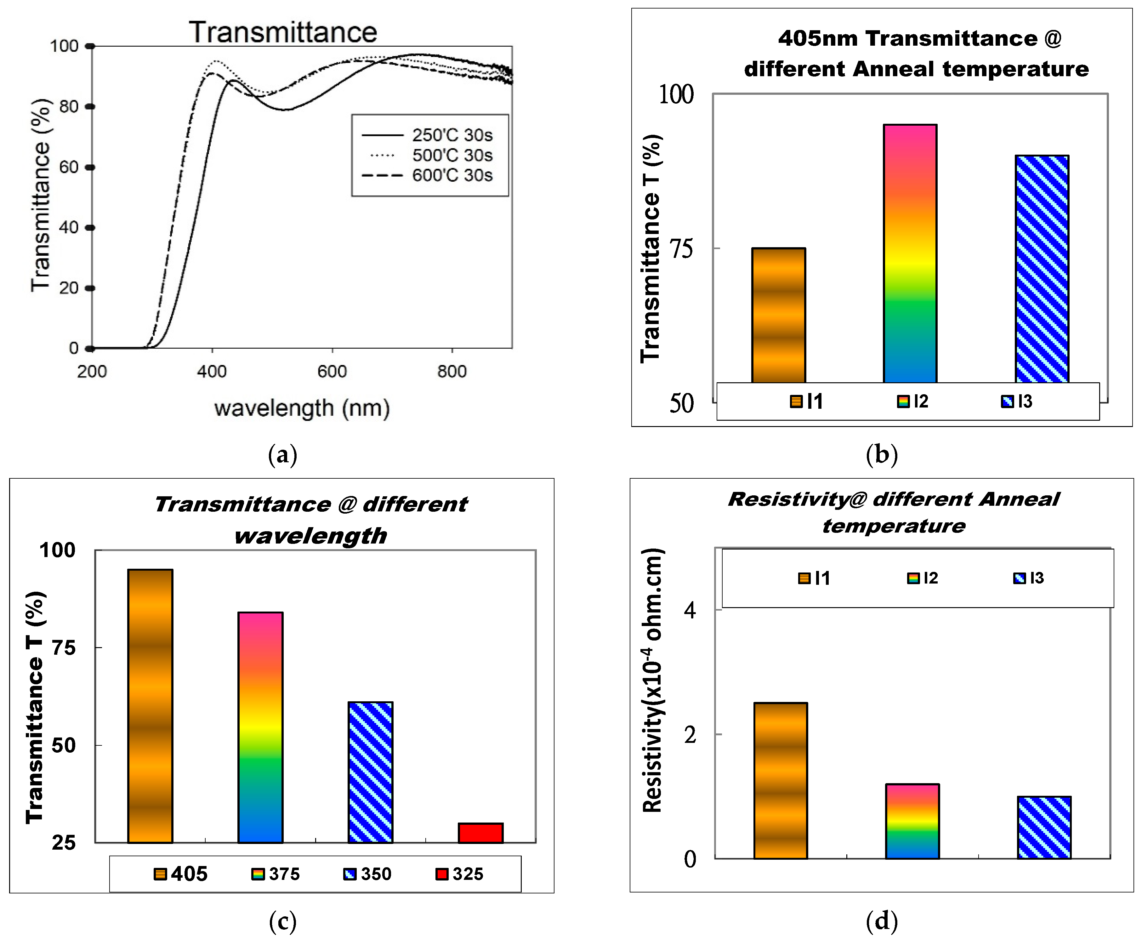
3.3. UV Transmittance and Resistivity Comparison of ITO Films at Different Annealing Temperatures

In Figure 7a, the transmittance spectra of the ITO films in the wavelength range from 200 to 900 nm are displayed. Figure 7b shows that the I2 sample with 500 °C 30 s PMA exhibited better performance in terms of UV transmittance at 405 nm compared to the I1 and I3 samples with 250 °C 30 s and 600 °C 30 s PMA, respectively. Figure 7c presents a comparison of the UV transmittance for the 500 °C 30 s PMA ITO thin film with different UV wavelengths of irradiation. Specifically, the UV transmittance of the I2 sample with 500 °C 30 s PMA was up to 95% at 405 nm wavelength, up to 85% at 375 nm, up to 60% at 350 nm, and up to 30% at 325 nm wavelength. The electrical resistivity value comparison for ITO thin film with different ITO anneal temperatures is shown in Figure 7d. The comparison of UV transmittance and resistivity of ITO films at varying annealing temperatures is in line with findings from prior research studies [20].

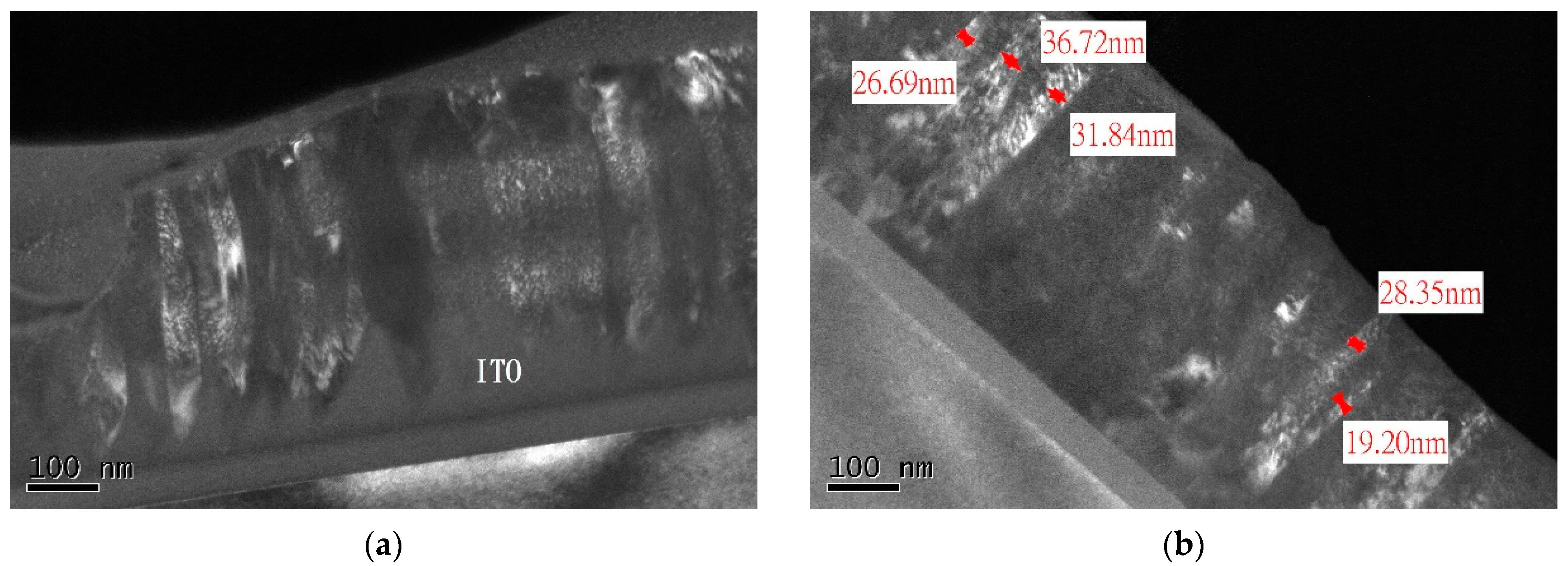
3.4. XRD and TEM Comparison of ITO Films at Different Annealing Temperatures

Figure 8 presents a comparison of the X-ray diffraction (XRD) analysis for ITO films with different annealing temperatures. The XRD analysis highlights the temperature-dependent crystallization of ITO films, as depicted in Figure 8. The peaks observed at around 2θ = 21.49°, 30.57°, and 51.00° correspond to the (2,1,1), (2,2,2), and (4,4,0) crystal structure planes of In2O3 [20,21,22,23,24]. Notably, the intensity of the (2,2,2) XRD diffraction peak of ITO films increases with the increase of post-anneal temperature. From the XRD analysis, it is evident that a phase change occurs during the post-anneal process in ITO.
Figure 9a–c present a comparison of the transmission electron microscopy (TEM) images for ITO films with different PMA temperatures. The TEM analysis reveals that the crystal structure of I1-ITO film is amorphous, mixed with incomplete nano-columnar (NCols) grains. Therefore, for the crystal structure of I2-ITO film, NCols grains become more complete and longer. However, for the crystal structure of I3-ITO film, columnar grains become wider and shorter. Notably, it appears that the ITO film annealed at 500 °C for 30 s PMA has longer and more complete NCols grains compared to the ITO films annealed at 250 °C for 30 s and 600 °C for 30 s PMA, as shown in Figure 9a–c [20,25,26,27,28,29,30].
Figure 9d–f present a TEM comparison of ZrAlOx/HfAlOx films with different PDA temperatures. The TEM results indicate that the ZrAlOx film structure remains almost amorphous even after annealing at 900 °C for 45 s. However, after annealing at 1000 °C for 45 s, the ZrAlOx film structure exhibits a partially smaller nanocrystallized structure. In contrast, the HfAlOx film structure shows a bigger nanocrystallized structure after annealing at 1000 °C for 45 s.

3.5. The Dependence of UV-Generated VT Increase on PGV for IAZAOS at Different UV Wavelengths

In Figure 10, the correlation between the UV-generated increase in VT and the PGV for an IAZAOS-I1Z2 sensor is depicted. Specifically, Figure 10a,b demonstrate this dependence under W405UV100 and W325UV100 irradiation, respectively. Previous studies [18,20] are consistent with this result. Notably, Figure 10 reveals that the UV-generated VT increase for the IAZAOS-I2Z2 sensor is 16 V and 12 V under W405UV100G25 and W325UV100G25 irradiation, respectively. By varying the PGVs during UV exposure, the sensitivity of the IAZAOS devices can be adjusted, rendering them suitable for diverse applications.

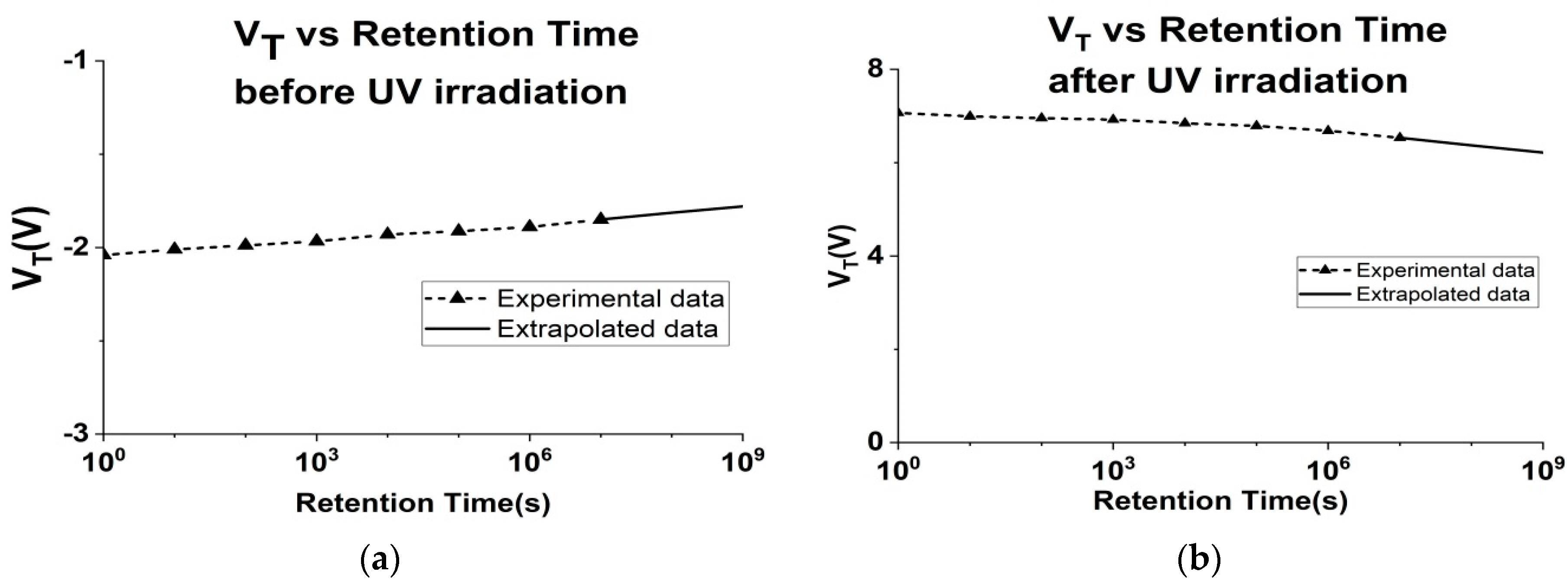
3.6. VT Stability vs. Retention Time

Figure 11a,b illustrate the VT time retention properties of an IAZAOS-I1Z2 UV TD NVM sensor before and after exposure to the W405UV100G15 irradiation conditions, respectively. Prior to UV exposure, intrinsic negative charges naturally tunnel into the ZrAlOx capture layer over time, causing the VT of the IAZAOS-I2Z2 UV TD NVM sensor to increase over time. However, after UV exposure, the negative charges induced by UV radiation gradually dissipate from the ZrAlOx capture layer over time, leading to a reduction in the VT of the IAZAOS-I2Z2 device over time.
Figure 12 illustrates the irradiation/refresh cycle characteristics of the IAZAOS-I2Z2/IAHAOS-I2H1 device. The upper curve is VT for the IAZAOS-I2Z2/IAHAOS-I2H1 device in W405UV100G15 irradiated state during each cycle, and the lower curve represents the VT of the IAZAOS-I2Z2/IAHAOS-I2H1 device in the erased state (refresh by NGV −15 V) during each cycle. As shown in the figure, the change of VT is not significant before 100 irradiation/erase cycles. The irradiation/refresh cycle characteristics performance of the IAZAOS-I2Z2 is better than the IAHAOS-I2H1 device.

4. Discussion

4.1. UV-Induced VT Shift in IAZAOS

In Figure 3, while the inversion responses are similar in both cases, the IAZAOS device shows greater dispersion in the accumulation region compared to the IAHAOS device, suggesting a higher density of border traps in the ZrAlOx trapping layer. Moreover, the higher accumulation capacitance of the IAZAOS device points to a higher permittivity of the ZrAlOx trapping layer [31,32].
In Figure 4, the positive shift in VT is consistent with previous research studies [18,20]. UV radiation generates electron–hole pairs in the substrate of the SONOS NVM-type UV TD sensor, which are then separated by a positive gate voltage (hereafter PGV). These negative charges are then swept over the SiO2 tunneling layer of the SONOS NVM-type UV TD and injected into the trapping layer of the SONOS NVM-type UV TD sensor. Some of these negative charges are captured by the trapping layer, leading to the permanent accumulation of negative charge in the capture layer of the SONOS NVM UV TD sensor.
Figure 6a demonstrates that the IAZAOS-I2Z2 device exhibits a larger UV-generated VT shift than the IAHAOS-I2H1 and IAZAOS-I2Z1 devices with W405UV100G25 irradiation. A previous study has noted that UV-generated charges can be trapped not only in trapping nanocrystals but also in amorphous regions of the trapping layer [18,19,20]. Therefore, it is known that the partially smaller nano crystallized trapping layer of IAZAOS-I2Z2 has a higher trap density than the complete whole amorphous trapping layer of IAZAOS-I2Z1 and the bigger nano crystallized IAHAOS-I2H1. It can be concluded that the partially smaller nano crystallized trapping layer of IAZAOS-I2Z2 with 1000 °C 30 s PDA has a larger trap density compared to the whole amorphous IAZAOS-I2Z1 with 900 °C 30 s PDA and the bigger nano crystallized IAHAOS-I2H1 with 1000 °C 30 s PDA. Previous studies [18,20] are consistent with this analysis.
Figure 6b compares the UV-generated VT change for various IAZAOS capacitor devices with different ITO PMA temperatures under W405UV100G15 irradiation conditions. It is observed that the VT change of IAZAOS-I2Z2 is the most significant compared to IAZAOS-I1Z2 and IAZAOS-I3Z2 under W405U100G15 irradiation conditions, as illustrated in Figure 6b. From the TEM analysis in Figure 9, the I2-ITO with longer and more complete NCols crystalline structure has longer and straighter UV photon-transmitting grains, while the I1-ITO with irregular and incomplete columnar crystal structures and the I3-ITO with equiaxed crystal structures have more irregular UV-photon-scattering grain boundaries. Previous studies [25,26,27,28,29,30] are consistent with this analysis.
Figure 6c indicates that the VT change of IAZAOS-I2Z2 with W405UV100G15 irradiation is approximately 1.1 times greater than that with W375UV100G15 irradiation, 1.3 times greater than that with W350UV100G15 irradiation, and 1.5 times greater than that with W325UV100G15 irradiation. Notably, the transmittance of I2 is as high as 95% at 405 nm wavelength, 85% at 375 nm, 60% at 350 nm, and 30% at 325 nm, as shown in Figure 6c. The UV-induced VT change of IAZAOS is closely related to the optical transmittance of ITO at different wavelengths of irradiation. It is important to note that even with W325UV100G15, the VT change of IAZAOS-I2Z2 remains as high as approximately 6 volts, as illustrated in Figure 6c. Previous studies [25,26,27,28,29,30] are consistent with this analysis. According to the information provided, the sensitive wavelength range of the IAZAOS-I2Z2 UV TD detector extends from visible light to 300 nm ultraviolet. That means it can detect both visible light and ultraviolet radiation. However, for accurate detection of UV radiation, visible light needs to be filtered out using a UV bandpass filter.
Figure 6d compares the CVSILC for IAZAOS and IAHAOS devices under different VG stresses for a 100-s duration. It was observed that the CVSILC of IAHAOS-I2H1 was almost 1000 times greater than that of IAZAOS-I2Z2 under −12 V VG stresses maintained for 100 s, as shown in Figure 6d. Specifically, the CVSILC of the IAHAOS-I2H1 device under −12 V VG stress for 100 s exceeded 1 mA, whereas the CVSILC of the IAZAOS-I2Z2 device under −12 V VG stress for 100 s remained less than 1 uA. Additionally, the CVSILC for the IAZAOS-I2Z2 device was less than 1 mA under the stress of VG −20 V for 100 s. The significant difference in GSILC between IAHAOS-I2H1 and IAZAOS-I2Z2 suggests that the smaller and more uniform grain size in the 1000 °C 30 s PDA ZrAlOx trapping layer facilitates the diffusion of oxygen into the grain and regions nearby grain boundaries. These diffused oxygen atoms can reduce the concentration of oxygen-vacancy defects and reduce the gate leakage current. The oxygen-vacancy concentration in the 1000 °C 30 s PDA ZrAlOx film is lower than that in the 1000 °C 30 s PDA HfAlOx film. The oxygen can be supplied by residual oxygen in the atmosphere or from the oxide film itself. Previous studies [31,32] are consistent with this analysis.

4.2. Sensitivity of IAZAOS-I2Z2

Based on the experimental results, the sensing performance of the SONOS-type UV TD sensor can be improved by using IAZAOS-I2Z2. The sensitivity of the IAZAOS-I2Z2 is greater than 16 KV·cm2/J with W405UV100G25 irradiation and is greater than 12 KV·cm2/J with W325UV100G25 irradiation. By varying the PGVs during UV exposure, the sensitivity of the IAZAOS devices can be adjusted, rendering them suitable for diverse applications. The resolution of the IAZAOS-I2Z2 is less than 10 nJ/cm2. The sensing range of the IAZAOS-I2Z2 is estimated to be around 10 nJ/cm2 to 1 J/cm2 for IAZAOS-I2Z2.

4.3. Model for UV-Induced VT Shift

To simulate the UV-Induced VT shift of the IAZAOS device, the author proposed a model (hereafter called the HWC-UVTD-ITO model) derived from the prior studies of the HWC-UV model [18,19,20].
deltaVT(D) = VT(D) − VT(0) = [(VG − Vo) × K]log(t × D)
The equation presented here consists of several variables. D represents the UV TD (mW·s/cm2), VT(D) is the VT after UV TD irradiation, VT(0) is the VT at D = 0, and VG is the PGV(V). The HWC-UVTD-ITO model used experimental curve fitting to derive three parameters: Vo, t, and K. Therefore, the t parameter represents the sum of trapping and de-trapping constants of electrons and holes from the trapping dielectric for specific devices. Vo is the minimum PGV for UV-induced charge injection into the gate dielectric. While K is the constant for specific devices. t is equal to 10 cm2/mW·s for IAZAOS-I2 for 405 nm irradiation in this study, 8 cm2/mW·s for 375 nm irradiation, 5.6 cm2/mW·s for 350 nm irradiation, and 1.7 cm2/mW·s for 325 nm irradiation condition in this study. Vo is equal to 3 Volt in this study. Moreover, K is equal to 0.25 for IAZAOS-Z2 devices in this study. VG is equal to 15 for G15 irradiation conditions in this study. Figure 13a–d show the comparisons of the measured and simulated curves of VT change as a function of UV TD for an IAZAOS-I2Z2 after W405G15, W375G15, W350G15, andW325G15 irradiation.

4.4. Model for VT Fading with Retention Time

To simulate the VT fading with retention time, the author proposed a model for VT fading with retention time (hereafter called HWC-VT fading model) derived from the prior studies of the HWC-UV model [18,19,20]:
VT(t) =VT(0) − [VT(0) × F1]ln(t) for VT(0) < 0
VT(t) =VT(0) − [VT(0) × F2]ln(t) for VT(0) > 0
“t” is the fading time; VT(0) is the VT at t = 0. F is the fading constant for specific devices. F1 is equal to 0.045 for VT(0) < 0. F2 is equal to 0.049 for VT(0) > 0 in this study. Figure 14 shows the comparisons of the measured and simulated curves of VT change as a function of retention time for an IAZAOS-I2Z2 before and after W405UV100G15 irradiation.

4.5. Irradiation/Fresh Cycle Endurance Characteristics

The device labeled IAZAOS-I2Z2 exhibits superior performance in terms of its VT degradation caused by irradiation/refresh cycle (endurance) as compared to the IAHAOS-I2H1 device. This is attributable to the smaller CVSILC of IAZAOS-I2Z2 in contrast to the larger CVSILC of IAHAOS-I2H1, which leads to inferior irradiation/erasure cycle characteristics of the IAHAOS-I2H1 device. Specifically, the VT change in the IAHAOS-I2H1 device remains relatively insignificant until the completion of 100 irradiation/refresh cycles, after which it undergoes a more drastic change.

5. Conclusions

The results of this study indicate that IAZAOS-I2Z2 displays a larger VT shift induced by UV irradiation in comparison to both IAHAOS-I2H1 and IAZAOS-I2Z1 devices. This can be attributed to the higher trap density in the partially smaller nanocrystallized IAZAOS-I2Z2 trapping layer as compared to the complete whole amorphous IAZAOS-I2Z1 trapping layer and the larger nanocrystallized IAHAOS-I2H1.
Additionally, the study found that the CVSILC of IAHAOS-I2H1 was almost 1000 times that of IAZAOS-I2Z2 under −12 V VG stresses maintained for 100 s. This suggests that the smaller and more uniform grain size of the 1000 °C 30 s PDA ZrAlOx trapping layer reduces the oxygen-vacancy defect concentration and gate leakage current.
Furthermore, IAZAOS-I2Z2 exhibits superior irradiation/refresh cycle endurance compared to the IAHAOS-I2H1 device due to its smaller CVSILC.
The sensitivity of IAZAOS-I2Z2 was found to be greater than 16 KV·cm2/J with W405UV100G25 irradiation and greater than 12 KV·cm2/J with W325UV100G25 irradiation, indicating the potential for improved sensing performance in SONOS-type UV TD sensors. However, the endurance characteristics of IAZAOS-I2Z2 over 100 irradiation/refresh cycles are not satisfactory and require further improvement in the future.
Improving the UV wavelength selectivity of the IAZAOS-I2Z2 UV TD detector can be challenging and may require changes in the detector design or materials. However, advances in technology and materials science may provide opportunities to improve the performance of the IAZAOS-I2Z2 UV TD detector in the future.

Author Contributions

Conceptualization, F.-C.J.; methodology, F.-C.J.; formal analysis, F.-C.J.; data curation, F.-C.J.; writing—original draft, W.-C.H.; writing—review and editing, W.-C.H.; visualization, F.-C.J.; supervision, F.-C.J. All authors have read and agreed to the published version of the manuscript.

Funding

This paper was funded in part by the National Science Council project (NSC) (NSC 109-2635-E-159-001-) and the National Nano Device Laboratories project (NDL) (JDP112-Y1-052).

Data Availability Statement

Not applicable.

Acknowledgments

The author would also like to thank National Nano Device Laboratories (NDL), National Tsing Hua University (NTHU), and National Chiao Tung University (NCTU) for providing the instruments for wafer fabrication and testing.

Conflicts of Interest

The authors declare no conflict of interest.

References

  1. D’Orazio, J.; Jarrett, S.; Amaro-Ortiz, A.; Scott, T. UV Radiation and the Skin. Int. J. Mol. Sci. 2013, 14, 12222–12248. [Google Scholar] [CrossRef] [Green Version]
  2. Amaro-Ortiz, A.; Yan, B.; D’Orazio, J.A. Ultraviolet Radiation, Aging and the Skin: Prevention of Damage by Topical cAMP Manipulation. Molecules 2014, 19, 6202–6219. [Google Scholar] [CrossRef] [PubMed]
  3. Oliveira, F.; Amaral, L.L.; Costa, A.M.; Netto, T.G. In vivo dosimetry with silicon diodes in total body irradiation. Radiat. Phys. Chem. 2014, 95, 230–232. [Google Scholar] [CrossRef]
  4. Sarrabayrouse, G.; Siskos, S. Low dose measurement with thick gate oxide MOSFETs. Radiat. Phys. Chem. 2012, 81, 339–344. [Google Scholar] [CrossRef]
  5. Karmakar, A.; Wang, J.; Prinzie, J.; De Smedt, V.; Leroux, P. A Review of Semiconductor Based Ionising Radiation Sensors Used in Harsh Radiation Environments and Their Applications. Radiation 2021, 1, 194–217. [Google Scholar] [CrossRef]
  6. Holmes-Siedle, A.; Adams, L. RADFET: A review of the use of metal-oxide-silicon devices as integrating dosimeters. Radiat. Phys. Chem. 1986, 28, 235–244. [Google Scholar] [CrossRef]
  7. Sze, S.M.; Ng, K.K. Physics of Semiconductor Devices, 3rd ed.; John Wiley & Sons: Hoboken, NJ, USA, 2006; p. 663. [Google Scholar]
  8. Pejović, M.M. P-channel MOSFET as a sensor and dosimeter of ionizing radiation. Electron. Energ. 2016, 29, 509–541. [Google Scholar] [CrossRef] [Green Version]
  9. Ho, W.S.; Lin, C.H.; Kuo, P.S. Metal Oxide Semiconductor UV Sensor. Proc. IEEE Sens. 2008, 8, 1584–1587. [Google Scholar]
  10. Oldham, T.R.; McLean, F.B. Total Ionizing Dose Effects in MOS Oxides and Devices. IEEE Trans. Nucl. Sci. 2003, 50, 483–499. [Google Scholar] [CrossRef]
  11. Jong, F.C.; Hsieh, W.C.; Lee, H.D.; Wu, S.C. UV Total Dose Nonvolatile Sensor Using Silicon-Oxide-Nitride-Oxide-Silicon Capacitor with Oxy-nitride as Charge-trapping Layer. Sens. Mater. 2018, 30, 1831–1839. [Google Scholar] [CrossRef]
  12. Hsieh, W.C.; Jong, F.C.; Tseng, W.T. Performance Improvement of SAONOS Device as UV-total-dose Nonvolatile Sensor with Al2O3/SiO2 Bilayer Blocking Oxide. Sens. Mater. 2020, 32, 2303–2310. [Google Scholar] [CrossRef]
  13. Tan, Y.N.; Chim, W.K.; Choi, W.K.; Joo, M.S.; Ng, T.H.; Cho, B.J. High-K HfAlO Charge Trapping Layer in SONOS-type Nonvolatile Memory Device for High Speed Operation. IEEE IEDM 2004, 4, 889–892. [Google Scholar]
  14. Yu, H.Y.; Li, M.F.; Kwong, D.L. ALD (HfO2)x (Al2O3) 1−x high-k gate dielectrics for advanced MOS devices application. Thin Solid Films 2004, 462, 110–113. [Google Scholar] [CrossRef]
  15. Zhu, W.J.; Tamagawa, T.; Gibson, M.; Furukawa, T.; Ma, T.P. Effect of Al Inclusion in HfO2 on the Physical and Electrical Properties of the Dielectrics. IEEE Electr. Device Lett. 2002, 23, 649–651. [Google Scholar] [CrossRef]
  16. Zhu, W.; Ma, T.P.; Tamagawa, T.; Di, Y.; Kim, J.; Carmthers, R.; Gibson, M.; Furukawa, T. HfO2 and HfAlO for CMOS: Thermal Stability and Current Transport. IEEE IEDM 2001, 1, 463–466. [Google Scholar]
  17. Zhang, G.; Samanta, S.K.; Singh, P.K.; Ma, F.J.; Yoo, M.T.; Roh, Y.; Yoo, W.J. Partial Crystallization of HfO2 for Two-Bit/Four-Level SONOS-Type Flash Memory. IEEE Trans. Electron Devices 2007, 54, 3177–3185. [Google Scholar] [CrossRef]
  18. Hsieh, W.C.; Lee, H.D.; Jong, F.C. An Ionizing Radiation Sensor Using a Pre-Programmed MAHAOS Device. Sensors 2014, 14, 14553–14566. [Google Scholar] [CrossRef] [PubMed] [Green Version]
  19. Hsieh, W.C. Performance Improvement of a Nonvolatile UV TD Sensor Using SAHAOS with a High Temperature Annealed, Partially Nano-Crystallized Trapping Layer. Sensors 2019, 19, 1570. [Google Scholar] [CrossRef] [Green Version]
  20. Hsieh, W.C.; Jong, F.C.; Tseng, W.T. Performance Improvement of Total Ionization Dose Radiation Sensor Devices Using IOHAOS with Enhanced UV Transparency ITO Gate. Coatings 2021, 11, 408. [Google Scholar] [CrossRef]
  21. Ghosh, A.; Mondal, A.; Murkute, P.; Lahiri, R.; Chakrabarti, S.; Chattopadhyay, K.K. GLAD synthesised erbium doped In2O3 nano-columns for UV detection. J. Mater. Sci. Mater. Electron. 2019, 30, 12739–12752. [Google Scholar] [CrossRef]
  22. Farvid, S.S.; Ju, L.; Worden, M.; Radovanovic, P.V. Colloidal Chromium-Doped In2O3 Nanocrystals as Building Blocks for High-TC Ferromagnetic Transparent Conducting Oxide Structures. J. Phys. Chem. C 2008, 112, 46. [Google Scholar] [CrossRef]
  23. Tandon, B.; Ashok, A.; Nag, A. Colloidal Transparent Conducting Oxide Nanocrystals: A New Infrared Plasmonic Material. Pramana-J. Phys. 2015, 84, 1087–1098. [Google Scholar] [CrossRef]
  24. Gao, M.Z.; Job, R.; Xue, D.S.; Fahrner, W.R. Thickness Dependence of Resistivity and Optical Reflectance of ITO Films. Chin. Phys. Lett. 2008, 25, 1380. [Google Scholar]
  25. Pokaipisit, A.; Horspath, M.; Limsuwan, P. Vacuum and air annealing effects on properties of indium tin oxide films prepared byion-assisted electron beam evaporation. Jpn. J. Appl. Phys. 2008, 47, 4692–4695. [Google Scholar] [CrossRef]
  26. Dobrowolski, J.A.; Ho, F.C.; Menagh, D.; Simpson, R.; Waldorf, A. Transparent, conducting indium tin oxide films formed on low or medium temperature substrates by ion-assisted deposition. Appl. Opt. 1987, 26, 5204–5210. [Google Scholar] [CrossRef]
  27. Wen, A.J.C.; Chen, K.L.; Yang, M.H.; Hsiao, W.T.; Chao, L.G.; Leu, M.S. Effect of substrate angle on properties of ITO films deposited by cathodic arc ion plating with In-Sn alloy target. Surf. Coat. Technol. 2005, 198, 362–366. [Google Scholar] [CrossRef]
  28. Chiou, B.S.; Tsai, J.H. Antireflective coating for ITO films deposited on glass substrate. J. Mater. Sci. 1999, 10, 491–495. [Google Scholar]
  29. Molzen, W.W. Characterization of transparent conductive thin films of indium oxide. J. Vac. Sci. Technol. 1975, 12, 99–102. [Google Scholar] [CrossRef]
  30. Meng, L.J.; Placido, F. Annealing effect on ITO thin films prepared by micro wave enhanced dc reactive magnetron sputtering for telecommunication applications. Surf. Coat. Technol. 2003, 166, 44–50. [Google Scholar] [CrossRef]
  31. Rahman, M.M.; Kim, D.H.; Kim, T.W. Border Trap Characterizations of Al2O3/ZrO2 and Al2O3/HfO2 Bilayer Films Based on Ambient Post Metal Annealing and Constant Voltage Stress. Nanomaterials 2020, 10, 527. [Google Scholar] [CrossRef] [PubMed] [Green Version]
  32. Jung, H.-S.; Lee, S.A.; Rha, S.H. Impacts of Zr Composition in Hf1−xZrxOy Gate Dielectrics on Their Crystallization Behavior and Bias-Temperature-Instability Characteristics. IEEE Trans. Electron Devices 2011, 58, 2094–2102. [Google Scholar] [CrossRef]
Figure 1. OM image of IAZAOS capacitor device.
Crystals 13 01092 g001
Figure 2. IAZAOS capacitor fabrication flow.
Crystals 13 01092 g002
Figure 3. Frequency-dependent C–V responses of (a) IAHAOS-I2H1 and (b) IAZAOS-I2Z2 in virgin state over the 1 kHz–100 kHz range.
Crystals 13 01092 g003
Figure 4. CG–VG curve for an IAZAOS-I2Z2 device before UV irradiation and after W405UV100G15 irradiation.
Crystals 13 01092 g004
Figure 5. (a) The dependence of the UV-generated VT increase on UV TD for an IAZAOS-I2Z2 sensor under W405G15 irradiation; (b) the dependence of the UV-generated VT increase on UV TD for an IAZAOS-I2Z2 sensor under W375G15 irradiation; (c) the dependence of the UV-generated VT increase on UV TD for an IAZAOS-I2Z2 sensor under W350G15 irradiation; (d) the dependence of the UV-generated VT increase on UV TD for an IAZAOS-I2Z2 sensor under W325G15 irradiation.
Crystals 13 01092 g005
Figure 6. (a) The UV-generated VT change comparison for various IAZAOS/IAHAOS devices with different PDA temperatures after W405UV100G25 irradiation; (b) UV-generated VT change comparison for various IAZAOS devices with different ITO PMA temperatures after W405UV100G15 irradiation; (c) the UV-generated VT change comparison for IAZAOS-I2Z2 devices after UV100G15 irradiation with different UV wavelength; (d) the CVSILC for IAZAOS-I2Z2/IAHAOS-I2H1 devices after different VG stress.
Crystals 13 01092 g006
Figure 7. (a) The UV transmittance spectra comparison for ITO thin film with different anneal temperatures; (b) the 405 nm UV transmittance comparison for ITO thin film with different anneal temperatures; (c) the UV transmittance comparison for I2-ITO thin film with different UV wavelength irradiation; (d) the resistivity comparison for ITO thin film with different ITO anneal temperatures.
Crystals 13 01092 g007
Figure 8. XRD analysis comparison of ITO films with different PMA temperatures.
Crystals 13 01092 g008
Figure 9. (a) TEM image of ITO with 250 °C 30 s PMA (dark-field); (b) TEM image of ITO with 500 °C 30 s PMA (dark-field); (c) TEM image of ITO with 600 °C 30 s PMA (dark-field); (d) TEM image of AZAO with 900 °C 45 s PDA; (e) TEM image of AZAO with 1000 °C 45 s PDA; (f) TEM image of AHAO with 1000 °C 45 s PDA.
Crystals 13 01092 g009aCrystals 13 01092 g009b
Figure 10. The dependence of the UV-generated VT increase on PGV for an IAZAOS-I2Z2 sensor (a) under W405UV100 irradiation and (b) under W325UV100 irradiation.
Crystals 13 01092 g010
Figure 11. The VT retention characterization curve for an IAZAOS-I2Z2 device: (a) before UV irradiation and (b) after W405UV100G15 irradiation.
Crystals 13 01092 g011
Figure 12. The VT decay under irradiation/refresh cycles endurance of (a) IAZAOS-I2Z2 device and (b) IAHAOS-I2H1 device.
Crystals 13 01092 g012
Figure 13. (a) The model of VT change as a function of UV TD for an IAZAOS-I2Z2 under W405G15 irradiation; (b) the model of VT change as a function of UV TD for an IAZAOS-I2Z2 under W375G15 irradiation; (c) the model of VT change as a function of UV TD for an IAZAOS-I2Z2 under W350G15 irradiation; (d) the model of VT change as a function of UV TD for an IAZAOS-I2Z2 under W325G15 irradiation.
Crystals 13 01092 g013
Figure 14. The model of VT retention characterization curve for an IAZAOS-I2Z2 device: (a) before UV irradiation and (b) after W405UV100G15 irradiation.
Crystals 13 01092 g014
Table 1. Comparison of semiconductor-based radiation sensors.
Sensing ElementSensing Principle SensitivityData StorageField Applications
Silicon diodeVoltage/Current transientsLowTemporaryHigh-dose/Ionizing radiation
Silicon PIN Voltage/Current transientsLowTemporaryHigh-dose/Ionizing radiation
RADFETThreshold voltage shiftLowTemporaryHigh-dose/Ionizing radiation
FOXFETThreshold voltage shiftLowTemporaryHigh-dose/Ionizing radiation
FGMOSThreshold voltage shiftHighPoor data retentionLow-dose/Non-ionizing radiation
SONOSThreshold voltage shiftHighGood data retentionLow-dose/High-dose/Ionizing/Non-ionizing radiation
Table 2. IAZAOS/IAHAOS devices prepared with various anneal processes.
SplitI2Z1I2Z2I2H1I1Z2I2Z2I3Z2
Gate conductor layer ITO PMA temperature (°C)500500500250500600
Gate conductor layer ITO PMA time (s)303030c303030
Gate conductor layer materialITOITOITOITOITOITO
Gate dielectric layer AZAO/AHAO PDA temperature (°C)90010001000100010001000
Gate dielectric layer AZAO/AHAO PDA time (s) 454545454545
Gate dielectric layer materialAZAOAZAOAHAOAZAOAZAOAZAO
Table 3. Symbol list of various UV TD, PGV, and UV wavelength conditions on IAZAOS UV TD sensor.
SymbolUV TD (mW·s/cm2)PGV (V)UV Wavelength (nm)
W405UV0G15 0 mW·s/cm215 V405
W405UV100G15100 mW·s/cm215 V405
W375UV100G15100 mW·s/cm215 V375
W350UV100G15100 mW·s/cm215 V350
W325UV100G15100 mW·s/cm215 V325
W325UV100G25100 mW·s/cm225 V325
W405UV100G25100 mW·s/cm225 V405
Disclaimer/Publisher’s Note: The statements, opinions and data contained in all publications are solely those of the individual author(s) and contributor(s) and not of MDPI and/or the editor(s). MDPI and/or the editor(s) disclaim responsibility for any injury to people or property resulting from any ideas, methods, instructions or products referred to in the content.

