Abstract
In this work, we used the Direct Laser Writing Grayscale Photolithography technology to fabricate a normally-off p-GaN gate high-electron-mobility transistor with the air-bridge source-connection. The air-bridge source-connection was formed using the Direct Laser Writing Grayscale Photolithography, and it directly connected the two adjacent sources and spanned the gate and drain of the multi-finger p-GaN gate device, which featured the advantages of stable self-support and large-span capabilities. Verified by the experiments, the fabricated air-bridge p-GaN gate devices utilizing the Direct Laser Writing Grayscale Photolithography presented an on-resistance of 36 Ω∙mm, a threshold voltage of 1.8 V, a maximum drain current of 240 mA/mm, and a breakdown voltage of 715 V. The results provide beneficial design guidance for realizing large gate-width p-GaN gate high-electron-mobility transistor devices.
1. Introduction
Gallium nitride- (GaN) based high-electron-mobility transistors (HEMT) are promising candidates for high-power applications due to their superior material and device characteristics [1,2]. Two-dimensional electron gas (2DEG) is created and limited at the interface between AlGaN/GaN by the piezoelectric effect of the GaN/AlGaN heterojunction and the spontaneous polarization effect. Based on the conventional structure of AlGaN/GaN-channeled electrons, it allows only the construction of depletion-mode normally-on devices. D-mode devices must import a continuous negative gate voltage to realize device turn-off; hence, they need extra-complicated gate-driver circuitry. In order to achieve normally-off GaN HEMT, different technologies have been proposed, such as cascode configuration combining Si-based normally-off MOSFET and GaN-based normally-on HEMT, fluorine-ion-implantation gate HEMT, gate-recessed MIS (metal–insulator–semiconductor)-HEMT, and p-GaN gated HEMT. Among the various GaN devices, p-GaN gate HEMT have the advantage of a stable threshold voltage and high repeatability of the process and have been commercially accepted and adopted [3]. With the development of the high-current p-GaN gate HEMT, the source-connection technology has been utilized to realize the large gate-width device [4]. Several common interconnection methods are adopted in multi-finger devices: the dielectric-isolation connection, back-hole connection using Through Silicon Via (TSV), and air-bridge connection. The air-bridge source-connection is an effective method to connect the source in the large gate-width device with a multi-finger structure [5]. The source-connected air-bridge field plate (AFP), which jumps from the source over the gate and lands between the gate and drain, has been fabricated. Compared to HEMT with a conventional field plate, this AFP structure can result in a three-times-higher improvement in forward-blocking voltage, attain 375 V, 37% lower Ron,sp, and drain leakage current lower by one order of magnitude. Dora Y shows that slant-field-plate technology has been fabricated and proven to be very effective; the slant-field plate is self-aligned with the gate in a single-process step and is shown to support a breakdown voltage up to 1900 V [6]. The Coffie R model shows that transition angles of less than 30° (measured from the surface) can result in significant improvements in electric field management [7].
In this work, we demonstrated an air-bridge source-connection p-GaN gate HEMT, fabricated using Direct Laser Writing Grayscale Photolithography (DLWGP) technology. Through controlling a different intensity or dose of light, the DLWGP can expose different vertical depths of the photoresist of the same thickness to quickly obtain the air-bridge source-connection structure. Compared to the E-beam [8,9] and digital micromirror device (DMD) [10] that are reported so far, the DLWGP draws more attention because it is maskless, versatile for the various semiconductor materials, suitable for the fast iteration of prototypes, and so on. By utilizing the DLWGP technology, the multi-finger p-GaN gate HEMT with the air-bridge source-connection is well-presented. The fabrication processes are discussed, and the performances of the experimental device are characterized and analyzed.
2. Experiments
Two methods have been reported to realize the p-GaN gate structure. One is the selective epitaxy p-GaN layer on the surface of AlGaN barrier [11]. Interface pollution and hole concentration are major problems for selective epitaxy and result in this technology being difficult to widely fabricate at present. The other one is whole epitaxy, growing a whole p-GaN layer on the surface of AlGaN and removing p-GaN layers except for the gate, using etching with which a channel of 2DEG could reappear except for the gate. Adopting this method to realize p-GaN gate structure has the advantage of stable threshold voltage and a repeatable process of fabrication, and it is widely applied to fabricate E-mode HEMT.
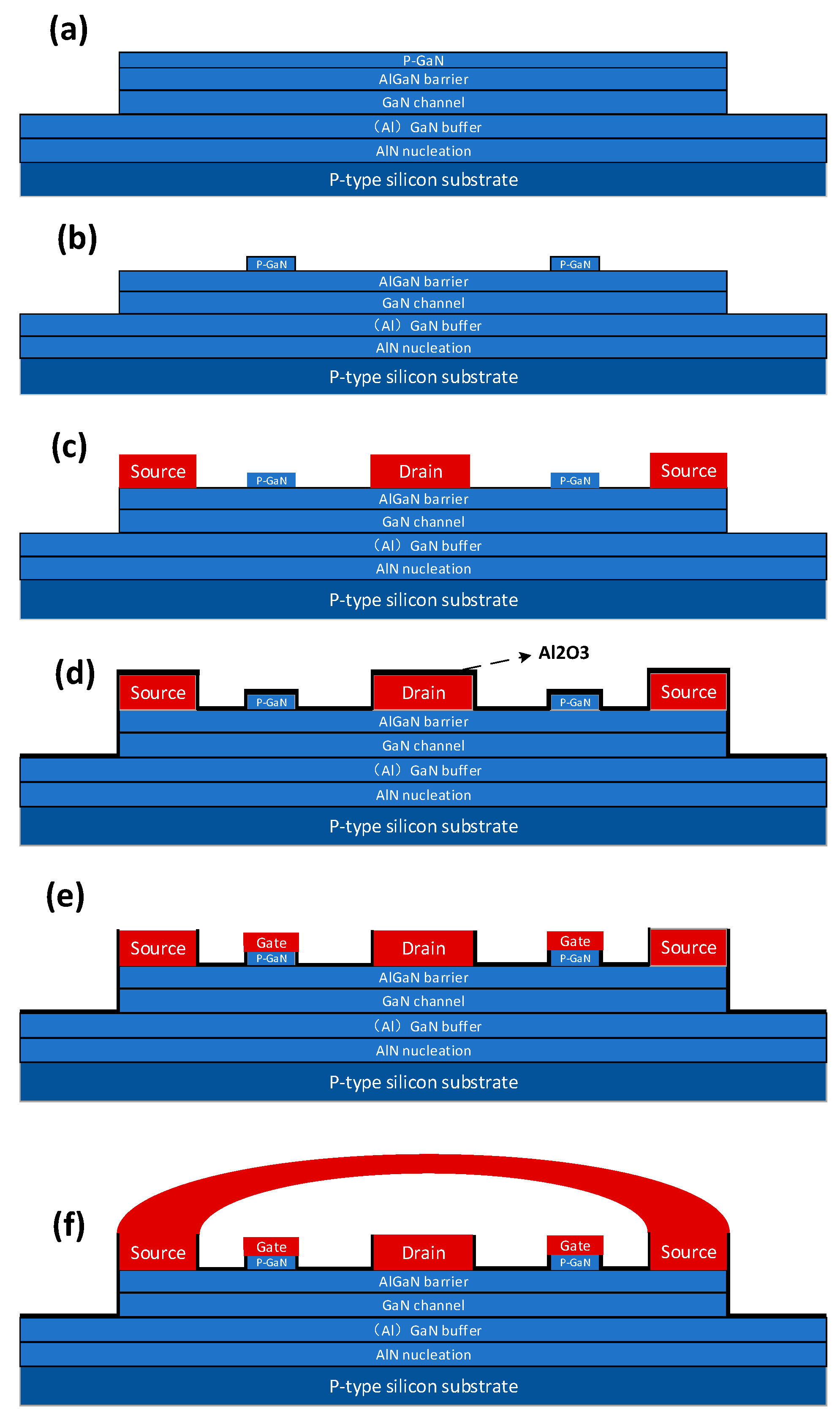
In this paper, we fabricated an enhanced HEMT device by adopting the etching p-GaN method. The process modules for the (E-mode) GaN HEMT device fabrication included device isolation, p-GaN gate formation, source and drain ohmic contact, gate Schottky contact, surface passivation, and DWLGP air-bridge connection (as shown in Figure 1). We will focus on several key process technologies for p-GaN HEMT.
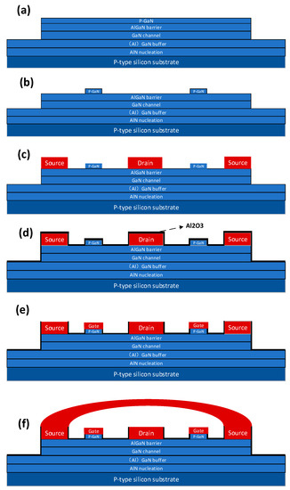
Figure 1.
Fabrication processes of the air-bridge common-source normally-off Mg-GaN/AlGaN/GaN HEMT (a) mesa etching; (b) p-GaN etching; (c) evaporated Ti/Al/Ni/Au and annealing treatment (d) ALD-Al2O3 passivation/dielectric; (e) removal the top of the p-GaN, drain and source passivation, and evaporated Ni/Au and pad metal. (f) air-bridge common-source using grayscale technology.
The p-GaN/AlGaN/GaN heterostructures were grown using MOCVD on 800 µm Si substrate. The layer stack consisted of a 2 nm AlN nucleation, a 4 µm (Al)GaN buffer, a 200 nm GaN channel, a 15 nm AlGaN barrier (with Al content of 0.2), and a 70 nm thickness Mg-doped p-GaN cap layer with a doping concentration of 1× 1018 cm−3.
2.1. Device Isolation
Device isolation is a step in the fabrication process to separate adjacent devices by destroying the electronic channel and reducing the impact of current leakage between devices. There are two common methods to realize device isolation. The first method is by adopting ion-implantation equipment to isolate the active area of the p-GaN HEMT device (implantation ion species including B+, N+, and He+). In this way, the channel of the heterojunction interface is destroyed with incident ions and realizes the isolation of devices. The ion-implantation process generally adopts several steps (implant energy gradually increasing). The advantage of the ion-implantation method is that the device surface stays flat after ion implantation, and the process is simple. The disadvantages are the high expense of the equipment, and that the injection energy is too large, which will cause the denaturation of the photoresist, and the subsequent removal of the denaturation of the photoresist raises the high requirements.
The second method adopts Inductively Coupled Plasma dry etching to destroy GaN channels outside the active area (requiring an etching depth far greater than the channel depth). After that, there is the forming of a mesa structure with a large height difference and without an electronic channel around it to achieve separation and isolation between devices. Among them, the Reactive Ion Etching (RIE) and Inductively Coupled Plasma (ICP) dry etching machines are the most widely used etching methods in GaN materials. The advantages of adopting a dry etching method to form mesa isolation are the simple process, the fact that it is easy to realize, and the low expense of the equipment. GaN dry etching using ICP has a physical bombardment and chemical reaction in which a chlorine base plays a major role in the chemical reaction.
In addition to the choice of chemistries employed, etching features and etching rate are affected by the gas flow, antenna RF Power, bias RF power, chamber pressure, and so forth. The chamber pressure influences the etching rate. Increasing the chamber pressure (higher than 30 mTorr) will cause the mean free path of the reactive molecules to shorten, plasma kinetic energy to reduce, and the physical bombardment etching rate to decline. Adopting the dry etching mesa method achieves isolation, and the adjacent device relies on the big resistivity of the buffer-layer material. When using the dry etching mesa for isolation, it should be noted that the thickness of the photoresist at the edge of the mesa is less than the flat photoresist, which will cause difficulty in metal lift-off. In the process of mesa etching, the corresponding marks are prepared together with the mesa etching. The area between the marks and the surrounding etched surface forms an obvious height difference to provide mark recognition for later alignment. This process is unsuitable for metal to mark because subsequent high-temperature annealing above 800 °C is required. The high temperature will damage the shape of the mark, which is inconvenient for the subsequent alignment.
2.2. p-GaN Gate Formation
Due to the need to achieve enhanced devices (normally-off HEMT), there are four ways to achieve enhanced devices described. P-GaN gate achieves enhanced HEMT; this device was adopted due to stable threshold voltages, which p-GaN gate had shown great potential for in GaN power device applications, and it had been commercialized [12]. The p-GaN layer lifts the energy bands of AlGaN, causing the 2DEG to disappear. In the process of fabricating the p-GaN gate device, the p-GaN layer other than the gate region was removed using ICP dry etching, and 2DEG reappeared. P-GaN etching is the key process in the fabrication of p-GaN gate devices and precisely controls the etching depth of the p-GaN cap layer as necessary. The residual p-GaN layer will deplete the 2DEG density, resulting in a decrease in the current density. Likewise, the over-etching of the AlGaN barrier layer will also decrease the current density due to it decreasing the polarization effect [13]. Therefore, the mesa etching recipe was unsuitably used for p-GaN etching. We need to optimize the p-GaN/AlGaN etching selection ratio. Two methods are recommended to achieve selective dry etching. One is fluorine-based chemical etching and the other is oxygen-based chemical etching. Both achieve a large p-GaN/AlGaN etching ratio by reducing the AlGaN etching rate.
Chang YC showed that adopting the Cl2/BCl3/SF6 mixed gas plasma self-terminating dry etching technique fabricated normally-off p-GaN HEMT devices [14]. This etching technique features accurate etching depth control and low surface-plasma damage. When SF6 reaches the AlGaN layer, fluorine-based gas reacts with Al and forms non-volatility AlF3 on the AlGaN surface, which significantly reduces the etching rate of the AlGaN layer, thus achieving selective etching of p-GaN over AlGaN. After self-terminating etching, the thin AlF3 layer on the surface was removed using a Buffered Oxide Etchant (BOE).
The other option is adopting oxygen and chlorine-based mixed gas. Taube A presented the results of the development of the selective etching of p-GaN over AlGaN in Cl2/Ar/O2 ICP plasma for the fabrication of normally-off p-GaN gate GaN HEMT using a laser reflectometry system for the precise control of the etched-material thickness [15]. By optimizing etching process parameters such as oxygen flow, ICP power, and chamber pressure, the high-etching selectivity of p-GaN and AlGaN was obtained, with values up to 56:1. The formation of thin Al2O3 surface passivation layers on the AlGaN surface was in an atmosphere containing oxygen, which is strongly resistant to etching and leads to a low etching rate of AlGaN. Increasing O2 flow (0–5 sccm) resulted in a decrease in etching rates for both GaN and AlGaN. The selectivity was increased with an O2 flow range of 0–2 sccm, but an O2 flow of more than 3 sccm while etching caused selectivity to begin to descend.
In this paper, we used a Cl2/O2/Ar mixture gas for the selective etching of the p-GaN layer. Firstly, we used Plasma Enhanced Chemical Vapor Deposition (PECVD) to deposit a 200 nm SiO2 protective film in the active region. The SiO2 film above the gate region was protected by the photoresist, and the non-gate region SiO2 was etched using CF4-based ICP. After removing the photoresist, the p-GaN was removed except in the gate region using the high-selection ratio of mixed-gas-based ICP. Finally, we soaked the BOE to remove the SiO2 protective film above the gate.
2.3. Ohmic Contacts
The source and drain of the Ohmic contact are the key steps in the preparation of GaN HEMT. A typical Ohmic contact is widely adopted using an electron beam to vaporize four layers of Ti/Al/Ni/Au metals and quickly anneal under the protection of nitrogen or other inert gases at high temperatures above 800 °C. Among them, the Ti-based layer metal plays a dominant role and reacts with the GaN surface N to form TiN at high temperatures, increasing the nitrogen vacancy at the interface, which leads to the thinning of the electron tunneling barrier [16]. However, single-layer Ti is easy to oxidize, so it is necessary to add Au metal to protect Al metal from oxidizing. Due to the strong downward diffusion of Au metal, a layer of Ni metal is inserted as a metal barrier layer in order to prevent the Au from diffusing with the Ti/Al. The Ohmic contact formed using this method is of low resistance and is easy to implement. Adopting Au-free metal stacking to make Ohmic contacts is strongly pursued at present as Au-free reduces expense, and Au is incompatible with the CMOS process. W Liang et al. presented a low Ohmic-contacts resistance formed with sidewall contacts with an Ohmic recess. Due to the direct sideways contact, which reduced the resistance of tunneling through the AlGaN barrier, it was believed to be a more efficient carrier transport mechanism [17].
In this paper, we adopted a lift-off metal method to fabricate source and drain ohmic metal. Coating the photoresist, the photoresist of the source and drain was removed using exposure and developer. The source and drain of the AlGaN barrier layer were thinned using Cl2-based ICP before metal evaporation to reduce contact resistance. The metal stack of Ti/Al/Ni/Au was evaporated in the source and drain region using electron beam evaporation. Soaking in acetone lifted off non-source/drain metal. Finally, annealing at 850 °C for 30 s in the ambient of N2 was performed to form the Ohmic contact.
2.4. Surface Passivation
The passivation layer is an essential step in the HEMT power-device process to protect the device from external influences and repair device performance. GaN device surface state is a complicated problem. These surface states may come from suspended bonds of surface atoms, plasma damage during etching p-GaN, surface pollutants, and so on. Vetury R showed surface states in the vicinity of the gate trap electrons and the depletion of channel electrons, which thus acted as a negatively charged virtual gate, which would cause current collapse [18]. A suitable passivation layer is needed to stabilize device performance and reliability. Plasma Enhanced Chemical Vapor Deposition (PECVD), Atomic Layer Deposition (ALD), and Low Pressure Chemical Vapor Deposition (LPCVD) are commonly used to prepare passivation layers of devices. At present, it has been explored that the insulation material widely used in the passivation layer of HEMT devices, including SiO2, Si3N4 [19], and Al2O3 [20]. In addition, GaN can be oxidized in the air forming a layer of gallium sub-oxide (GaOx) on the surface. Its oxidized defect surface state will lead to a gate leakage current. Bae. C proposed a plasma-assisted oxidation method before PECVD to significantly reduce defect state densities [21]. Compared with directly growing the passivation layer, plasma-assisted oxidation before the PECVD method reduced the gate-leakage current because adequate plasma oxidation transformed gallium sub-oxide (GaOx) into high-quality insulation materials.
In this paper, we deposited a high-quality Al2O3 passivation layer through ALD. Due to the ALD Self-limiting Reaction characteristic, the film of the Al2O3 passivation layer was deposited one by one. The main advantage of the ALD compared to other equipment is the high coverage and quality to better isolate the device from the external environment. We could control the thickness of the passivation layer by controlling the number of layers deposited.
2.5. Schottky Gate Metal
With normally-off devices with p-GaN layers, we usually steamed high-work function metal on the gate to form Schottky contacts. The difference in metal and semiconductor barrier height depends on the difference between the work function of the metal and the electron affinity of the semiconductor. With fixed gate voltage, the leakage current of the gate can be reduced effectively by increasing the height of the Schottky barrier. Therefore, some high-work function metals such as Ni, Ti, and W were used to prepare the Schottky contact-based metal. Single Ni metal is easily oxidized by air, so it is necessary to steam Au metal behind Ni to protect against oxidation while reducing the gate resistance.
Lu X et al. reported adopting a two-step process combining a pre-gate surface treatment and post-gate annealing to reduce the off-state leakage current in HEMT [22]. The post-gate annealing process reduced the vertical tunneling leakage current by improving the Schottky contact quality of the transistor gate. The device’s off-state leakage current was reduced by about 7 orders.
Considering that the Schottky metal needs better adhesion on the p-GaN surface to prevent the metal from falling off in the subsequent process, we chose the stack of Ni/Au metal as the Schottky metal. After we deposited the passivation layer, we coated the photoresist on the surface of the passivation layer and removed the upper photoresist of source/drain and p-GaN using exposing and developing. Then, we used Cl2-based ICP to remove the upper of p-GaN Al2O3 passivation. The stack of Ni/Au gate metals was deposited above the p-GaN gate to form the Schottky contact using Electron beam evaporation while the photoresist protected the non-gate regions.
2.6. Pad Metal
In order to conveniently test the performance of the ten-finger gate device, we needed to connect all the gates and drains of the device to a large enough Pad metal through metal lines. It is worth noting that the surface of Ohmic metal was too rough after annealing, and we cautiously used Ohmic metal as the Pad metal, which can cause bad contact between the probe and Pad during testing. Therefore, we prepared new Pad metal of source, drain, and gate using Electron Beam Evaporation while the drain and gate of the device were, respectively, connected to the corresponding Pad.
2.7. Air-Bridge Source-Connection with Direct Laser Writing Grayscale Photolithography
In the preceding process, the gate and drain electrode of devices had been connected to the corresponding Pad metal with metal lines. In this case, the source electrode of the device was without a connected path to the source Pad metal, so it needed to be connected from the second plane to avoid a short circuit. In this paper, the source of the device was directly connected to the pad from the top of the device using air-bridge-connect technology. In this paper, we proposed that fabricated air-bridges were adopted with the grayscale exposure method. Compared with other methods, the grayscale exposure method can fabricate a more flexible vertical design of air-bridges, and the fabrication of the grayscale exposure method is simpler.
In this work, we adopted the Heidelberg DWL66+ equipment grayscale-exposure mode to fabricate the air-bridge source-connection. This DWL66+ supports a minimum structure size of 0.3 µm, 0.6 µm, and 1 µm. The 0.3 µm minimum-size writing speed corresponded to 3 mm2/min, and the 0.6 µm minimum-size writing speed corresponded to 13 mm2/min. With both more quickly obtaining a 3D structure and supplying the demand of the design minimum line, we adopted a 0.6 µm minimum line-width gray mode. Standard and advanced grayscale modes were 128/256 gray levels, respectively. Moreover, the DWL66+ output a 405 nm light source using a diode laser (300 mw maximum output power). This DWL66+ supplied the air-gauge or optical autofocus for the exposure of small samples (less than 10 mm).
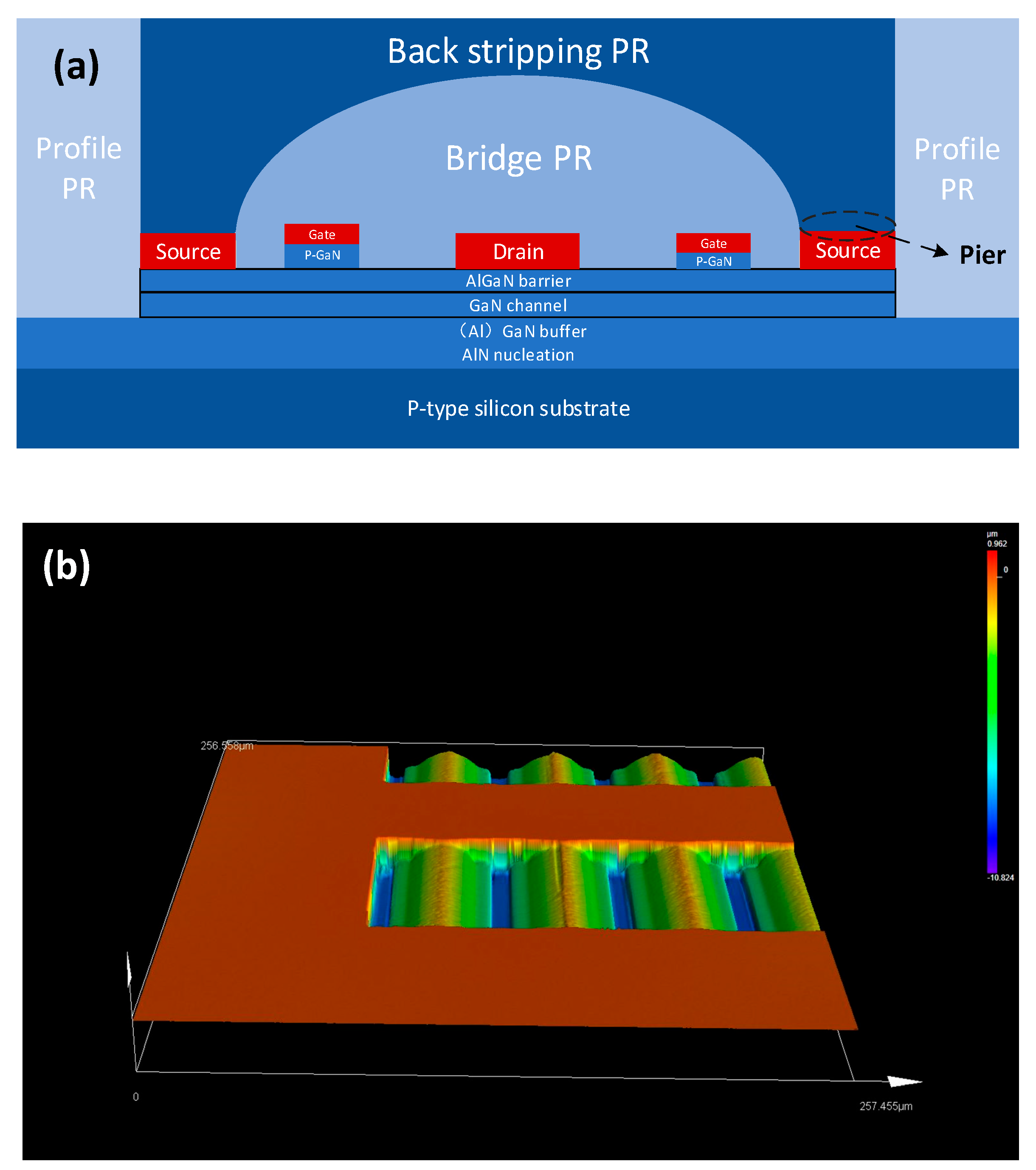
According to the DLWGP exposure principle, the upper part of the photoresist is first illuminated; hence, some 3D structures are impossible to achieve using the grayscale-exposure mode. The photoresist structure of the air-bridge support layer met the requirements for grayscale lithography, which can be decomposed into three parts, as shown in Figure 2a: pier, bridge photoresist, and the surrounding photoresist areas. Therein, the pier part must be fully exposed, and the part of the span bridge with curved exposure energy and the surrounding sacrificial photoresist part are unexposed in DLWGP mode. When designing the gray-exposure map of the air-bridge structure, we can simply divide the 3D structure into a 2D distribution map and height value. At present, the mainstream layout software is not compatible with gray value design, so we needed to design the bmp map through another pixel software. When we design a bmp map, we must follow the DLWGP conversion graph paper rule (one pixel is equal to 100 nm, and the center of the pixel map corresponds to the center of exposure) to plan the air-bridge structure distribution map; otherwise, we are unable to align the previous layer. In addition to locating the location of the air-bridge, we also need to set the gray value of the bridge and pier. In DWLGL mode, this device will divide the laser energy into 256 equivalencies (corresponding to 256 gray steps); the 255 value corresponds to the full value of the exposure power, and the 0 value corresponds to no exposure. Based on the criterion that the photoresist thickness of 6.9 µm corresponds to every grayscale value of 27 nm, the bridge camber is realized by designing a curve gradient gray value. After designing the bmp diagram, we can adjust the DWLGP.

Figure 2.
(a) grayscale exposure photoresist chart (b) laser scanning confocal microscope view 3D photoresist structure.
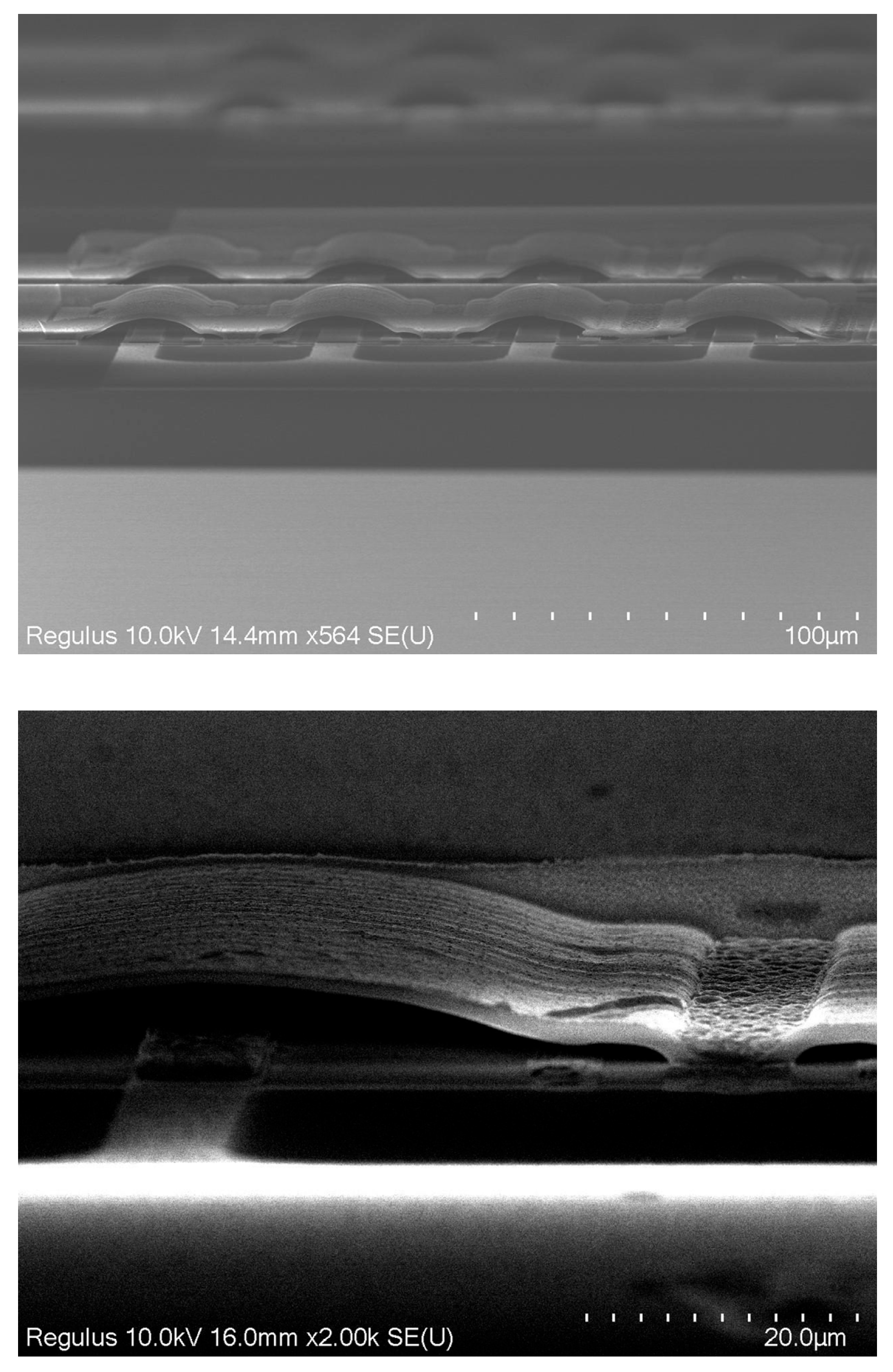
In order to obtain a metal bridge of sufficient thickness, we spun a coated target thickness of 6.9 µm AZ4562 photoresist. The appropriate gray exposure parameters were used to mold the photoresist for 3D exposure. After exposure, the photoresist was immersed in the newly configured developer (1:4/400 K: water) for 4 min. The developer removed the upper layer of the sensitive photoresist, and the 3D photoresist morphology could be scanned using a laser confocal microscope, as shown in Figure 2b. We could measure the line-width at the pier to meet our design requirement that the grid is still protected by the photoresist. Then we evaporated Ti/Al 20/1500 nm metals through electron beam deposition. It was soaked in acetone for 1 h, and the surrounding metals were taken off as the photoresist dissolved in the acetone. The remaining metal bridge structure (Figure 3) was observed through SEM, of which the air-bridge spans the grid and drain above to connect adjacent sources.
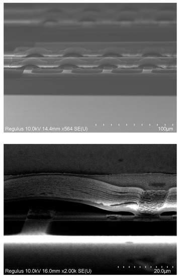
Figure 3.
Ten-finger air-bridge device SEM.
3. Results
We fabricated a ten-finger common-source HEMT with an air-bridge and a gate length of LG = 4 µm; the distance between the gate and source was LGS = 4 µm, and the distance between the gate and drain was LGD = 12 µm. In order to connect two adjacent sources (distance was 40 µm), a 40 µm span bridge with a source field plate structure was made through DWLGP.
The ten-finger devices connected with the air-bridge had good output performance. The measured output I-V characteristics of ten-finger common-source HEMT with air-bridge: VGS was kept ordinally from 0 to 8 V (step 2 V), VDS was swept from 0 to 20 V, and the source was tied to the ground. Their I-V characteristics were shown in Figure 4a; the saturation current of the devices was 240 mA/mm, and on-resistance was 36 Ω∙mm. The measured threshold voltage (VTH): VDS was kept at 10 V, VGS was swept from 0 to 5 V, and the source was tied to the ground. When it measured ID at 1 mA/mm, the corresponding VGS was the threshold voltage of the device. VTH = 1.8 V (measured at ID = 1 mA/mm) was shown in Figure 4b. The success of the ten-finger device was dependent on the stability of grayscale exposure, which the ten-finger device adopted a continuous air-bridge method to connect the source. It performed that fabricating the air-bridge through DWLGP had an excellent success rate. Up to now, without a bridge collapse after metal take-off, it indicated that the designed bridge structure had excellent reliability. It is noteworthy that when adopting the DWLGP method to mold the bridge, we need to control the exposure dose; too large of an exposure dose may expose the gate and directly connect the source to the grid after evaporating the metal, so the dose needs control within 10 mj. In order to ensure the pier line-width, it is necessary to use a laser scanning confocal microscope to view the photoresist morphology characteristics after the photoresist grayscale is exposed and developed. Incidentally, this laser scanning confocal microscope did not negatively affect the 3D photoresist structure.
Shock ionization and electron penetration are known to be the two most well-known physical mechanisms for the breakdown of HEMT devices [23,24]. There was a large peak at the gate electrode edge, especially if the gate was near the drain edge. If this large electric peak is not treated properly, it will cause electron penetration and the early breakdown of the device. In the design of a large-span bridge, the oblique floating-source field-plate structure is cleverly designed at the gate near the drain. It helps us to alleviate the electric field peak at the gate edge, which leads to significant breakdown voltage improvement. It can be seen from Figure 4c that the air-bridge floating-source field-plate structure HEMT had a high breakdown voltage: VBR = 715 V; the breakdown voltage measurements were performed using the Agilent B1505A semiconductor parameter analyzer. For the breakdown voltage tests, we set the maximum voltage and current limit of the test at 1200 V and 1 mA, VGS was set at 0 V, the source terminal was grounded, and VD increased from 0 V (step = 5 V). During the measurements, the devices were covered with Fluorinert.
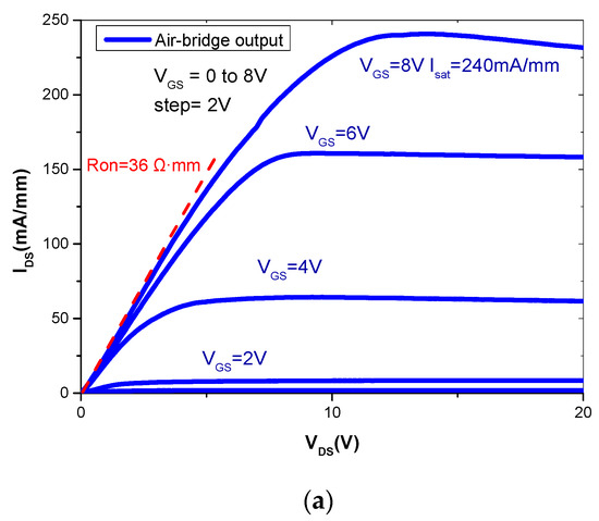
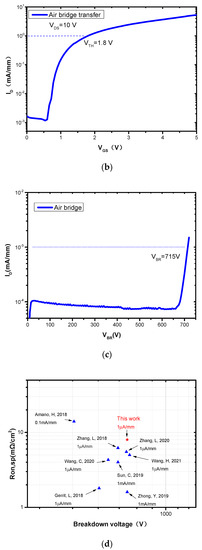
Figure 4.
(a) ten-finger air-bridge normally-off I-V output, VGS from 0 to 8 V (step 2 V), and VDS from 0 to 20 V; (b) measured DC I-V transfer characteristics of ten-finger air-bridge normally-off structure. VDS = 10 V; (c) Measured off-state characteristics of the fabricated ten-finger common-source HEMT breakdown voltage; (d) Ten-finger common-source HEMT VBR and Ron,sp comparisons with other p-GaN HEMT works [25,26,27,28,29,30,31,32].

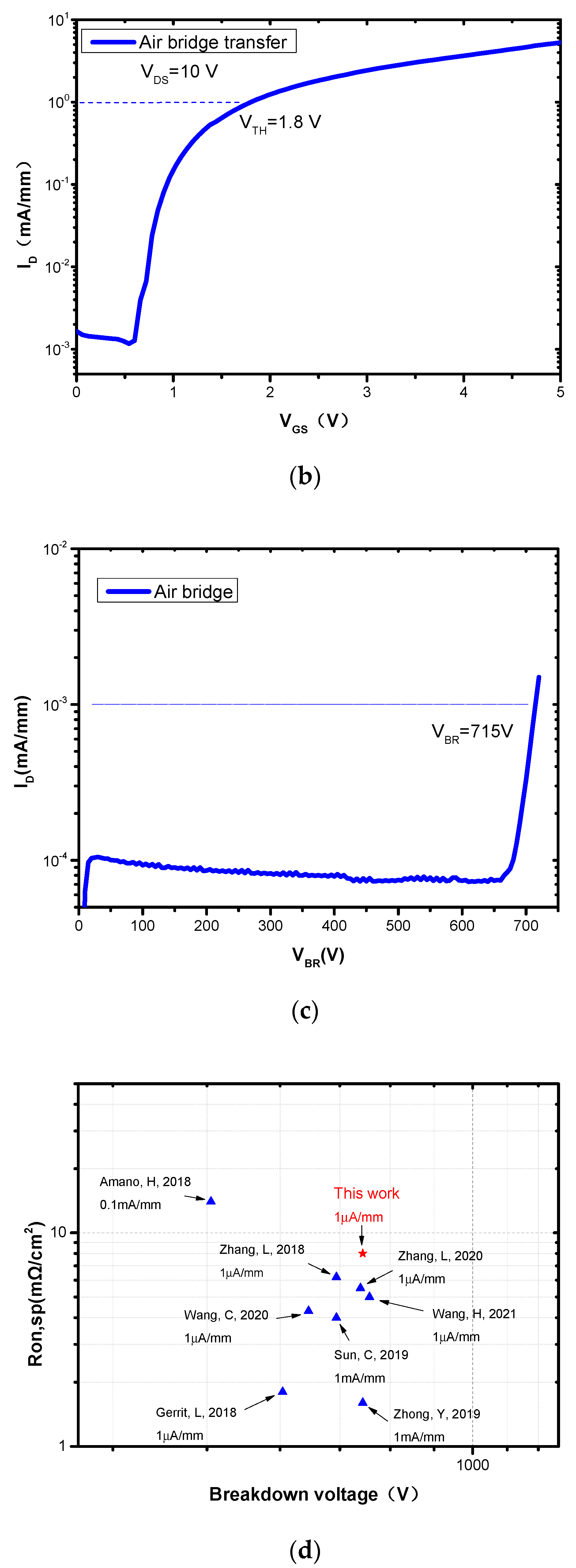
Figure 4d shows the proposed device against other p-GaN HEMT on the Si substrate reported [25,26,27,28,29,30,31,32]. The high-specific Ron (Ron,sp) of our device was attributed to the excessive etching of the source/drain of the AlGaN layer before metal evaporation, leading to the increase in ohmic contact resistance. This could be improved by optimizing etching time in the future. The competitive VBR could be attributed to the effective reduction in the high electric field crowded near the gate by using an air-bridge field plate. Compared to the AlGaN/GaN device (VBR = 375 V) with an air-bridge field plate [5], the fabrication of the ten-finger air-bridge connection of p-GaN devices has a higher breakdown performance that may be attributed to the longer distance between the source and drain.
4. Conclusions
We confirmed the feasibility of the common-source ten-finger device with an air-bridge prepared using DWLGP. This common-source ten-finger device has excellent output and transfer performance, and the use of the common source improves the utilization rate of the wafer. The use of a float-source field-plate structure can reduce the peak electric field at the gate edge and obtain a good breakdown voltage. The use of DWLGP-prepared air-bridges is suitable for the fast iteration of a prototype.
Author Contributions
Conceptualization, Y.Z. and G.D.; methodology, P.Y. and Y.Z.; software, F.W.; validation, Y.Z., C.Y. and J.H.; formal analysis, F.W. and X.W.; investigation, Y.Z. and Q.F.; resources, M.H., Y.W. and X.W.; data Y.Z. and F.W.; writing—original draft preparation Y.Z.; supervision, X.W., W.C., H.J., H.C. and Y.W.; project administration, Y.W. and W.X. All authors have read and agreed to the published version of the manuscript.
Funding
This work was supported in part by the Key-Area Research and Development Program of Guangdong Province, China, under Grant No.2020B010174001, and in part by the Guang-dong Basic and Applied Basic Research Foundation, China, under Grant No.2020A1515110567.
Data Availability Statement
The data presented in this study are available on request from the corresponding author.
Conflicts of Interest
The authors declare no conflict of interest.
References
- Chen, K.J. GaN-on-Si Power Technology: Devices and Applications. IEEE Trans. Electron Device 2017, 64, 779–795. [Google Scholar] [CrossRef]
- Efthymiou, L. On the physical operation and optimization of the p-GaN gate in normally-off GaN HEMT devices. Appl. Phys. Lett. 2017, 110, 123502. [Google Scholar] [CrossRef]
- Zheng, Z. Enhancement-Mode GaN p-Channel MOSFETs for Power Integration. In Proceedings of the 2020 32nd International Symposium on Power Semiconductor Devices and ICs (ISPSD), Vienna, Austria, 13–18 September 2020; pp. 525–528. [Google Scholar]
- Zhou, F. 1.2 kV/25 A Normally off P-N Junction/AlGaN/GaN HEMTs With Nanosecond Switching Characteristics and Robust Overvoltage Capability. IEEE Trans. Power Electron. 2022, 37, 26–30. [Google Scholar] [CrossRef]
- Xie, G. Breakdown-Voltage-Enhancement Technique for RF-Based AlGaN/GaN HEMTs With a Source-Connected Air-Bridge Field Plate. IEEE Electron Device Lett. 2012, 33, 670–672. [Google Scholar] [CrossRef]
- Dora, Y.; Chakraborty, A.; Mccarthy, L.; Keller, S.; Denbaars, S.P.; Mishra, U.K. High breakdown voltage achieved on AlGaN/GaN HEMTs with integrated slant field plates. IEEE Electron Device Lett. 2006, 27, 713–715. [Google Scholar] [CrossRef]
- Coffie, R. Slant field plate model for field-effect transistors. IEEE Trans. Electron Device 2014, 61, 2867–2872. [Google Scholar] [CrossRef]
- Kirchner, R. Bio-inspired 3D funnel structures made by grayscale electron-beam patterning and selective topography equilibration. Microelectron. Engineer. 2015, 141, 107–111. [Google Scholar] [CrossRef]
- Kim, J. Controlling resist thickness and etch depth for fabrication of 3D structures in electron-beam grayscale lithography. Microelectron. Engineer. 2007, 84, 2859–2864. [Google Scholar] [CrossRef]
- Totsu, K. Fabrication of three-dimensional microstructure using maskless gray-scale lithography. Sens. Actuators A Phys. 2006, 130–131, 387–392. [Google Scholar] [CrossRef]
- Ngo, T.H.; Comyn, R.; Chenot, S.; Brault, J.; Damilano, B.; Vezian, S.; Frayssinet, E.; Cozette, F.; Defrance, N.; Lecourt, F.; et al. Combination of selective area sublimation of p-GaN and regrowth of AlGaN for the co-integration of enhancement mode and depletion mode high electron mobility transistors. Solid-State Electron. 2022, 188, 108210. [Google Scholar] [CrossRef]
- Greco, G.; Iucolano, F.; Roccaforte, F. Review of technology for normally-off HEMTs with p-GaN gate. Mater. Sci. Semicond. Process. 2018, 78, 96–106. [Google Scholar] [CrossRef]
- Green, R.T.; Luxmoore, I.J.; Lee, K.B.; Houston, P.A.; Ranalli, F.; Wang, T.; Parbrook, P.J.; Uren, M.J.; Wallis, D.J.; Martin, T. Characterization of gate recessed GaN/AlGaN/GaN high electron mobility transistors fabricated using a SiCl4/SF6 dry etch recipe. J. Appl. Phys. 2010, 108, 013711. [Google Scholar] [CrossRef]
- Chang, Y.C.; Ho, Y.L.; Huang, T.Y.; Huang, D.W.; Wu, C.H. Investigation of Normally-Off p-GaN/AlGaN/GaN HEMTs Using a Self-Terminating Etching Technique with Multi-Finger Architecture Modulation for High Power Application. Micromachines 2021, 12, 432. [Google Scholar] [CrossRef]
- Taube, A.; Kamiński, M.; Ekielski, M.; Kruszka, R.; Jankowska-Śliwińska, J.; Michałowski, P.P.; Zdunek, J.; Szerling, A. Selective etching of p-GaN over Al0.25Ga0.75N in Cl2/Ar/O2 ICP plasma for fabrication of normally-off GaN HEMTs. Mater. Sci. Semicond. Process. 2021, 122, 105450. [Google Scholar] [CrossRef]
- Zhu, Y.; Huang, R.; Li, Z.; Hao, H.; An, Y.; Liu, T.; Zhao, Y.; Shen, Y.; Guo, Y.; Li, F.; et al. Interface analysis of TiN/n-GaN ohmic contacts with high thermal stability. Appl. Surf. Sci. 2019, 481, 1148–1153. [Google Scholar] [CrossRef]
- Wang, L.; Kim, D.H.; Adesida, I. Direct contact mechanism of Ohmic metallization to AlGaN/GaN heterostructures via Ohmic area recess etching. Appl. Phys. Lett. 2009, 95, 172107. [Google Scholar] [CrossRef]
- Vetury, R.; Zhang, N.Q.; Keller, S.; Mishra, U.K. Electrical and Computer Engineering Department, University of California, Santa Barbara, CA, USA The impact of surface states on the DC and RF characteristics of AlGaN/GaN HFETs. IEEE Trans. Electron Device 2001, 48, 560–566. [Google Scholar] [CrossRef]
- Geng, K.; Chen, D.; Zhou, Q.; Wang, H. AlGaN/GaN MIS-HEMT with PECVD SiNx, SiON, SiO2 as gate dielectric and passivation layer. Electronics 2018, 7, 416. [Google Scholar] [CrossRef]
- Xu, D.; Chu, K.; Diaz, J.; Zhu, W.; Roy, R.; Seekell, P.; Pleasant, L.M.; Isaak, R.; Yang, X.; Nichols, K.; et al. Performance enhancement of GaN high electron-mobility transistors with atomic layer deposition Al2O3 passivation. In Proceedings of the 2012 Lester Eastman Conference on High Performance Devices (LEC), Providence, RI, USA, 7–9 August 2012; IEEE: Piscataway, NJ, USA, 2012; pp. 1–3. [Google Scholar]
- Bae, C.; Lucovsky, G. Low-temperature preparation of Ga N-SiO2 interfaces with low defect density. I. Two-step remote plasma-assisted oxidation-deposition process. J. Vac. Sci. Technol. A Vac. Surf. Film. 2004, 22, 2402–2410. [Google Scholar] [CrossRef]
- Lu, X.; Jiang, H.; Liu, C.; Zou, X.; Lau, K.M. Off-state leakage current reduction in AlGaN/GaN high electron mobility transistors by combining surface treatment and post-gate annealing. Semicond. Sci. Technol. 2016, 31, 055019. [Google Scholar] [CrossRef]
- Uren, M.J. Punch-through in short-channel AlGaN/GaN HFETs. IEEE Trans. Electron Devices 2006, 53, 395–398. [Google Scholar] [CrossRef]
- Bahat-Treidel, E. Punchthrough-Voltage Enhancement of AlGaN/GaN HEMTs Using AlGaN Double-Heterojunction Confinement. IEEE Trans. Electron Devices. 2008, 55, 3354–3359. [Google Scholar] [CrossRef]
- Zhong, Y. Normally-off HEMTs With Regrown p-GaN Gate and Low-Pressure Chemical Vapor Deposition SiNx Passivation by Using an AlN Pre-Layer. IEEE Electron Device Lett. 2019, 40, 1495–1498. [Google Scholar] [CrossRef]
- Sun, C. Normally-off p-GaN/AlGaN/GaN high-electron-mobility transistors using oxygen plasma treatment. Appl. Phys. Express. 2019, 12, 051001. [Google Scholar] [CrossRef]
- Amano, H. The 2018 GaN power electronics roadmap. J. Phys. D Appl. Phys. 2018, 51, 163001. [Google Scholar] [CrossRef]
- Gerrit, L. Self-Aligned Process for Selectively Etched p-GaN-Gated AlGaN/GaN-on-Si HFETs. IEEE Trans. Electron Devices 2018, 65, 3732–3738. [Google Scholar]
- Li, Z. P-GaN Gate Power Transistor With Distributed Built-in Schottky Barrier Diode for Low-loss Reverse Conduction. IEEE Electron Device Lett. 2020, 41, 341–344. [Google Scholar]
- Li, Z. AlGaN-Channel Gate Injection Transistor on Silicon Substrate With Adjustable 4–7-V Threshold Voltage and 1.3-kV Breakdown Voltage. IEEE Electron Device Lett. 2018, 39, 1026–1029. [Google Scholar]
- Wang, C. E-Mode p-n Junction/AlGaN/GaN (PNJ) HEMTs. IEEE Electron Device Lette. 2020, 41, 545–548. [Google Scholar] [CrossRef]
- Wang, H. High-performance reverse blocking p-GaN HEMTs with recessed Schottky and p-GaN isolation blocks drain. Appl. Phys. Lett. 2021, 119, 023507. [Google Scholar] [CrossRef]
Disclaimer/Publisher’s Note: The statements, opinions and data contained in all publications are solely those of the individual author(s) and contributor(s) and not of MDPI and/or the editor(s). MDPI and/or the editor(s) disclaim responsibility for any injury to people or property resulting from any ideas, methods, instructions or products referred to in the content. |
© 2023 by the authors. Licensee MDPI, Basel, Switzerland. This article is an open access article distributed under the terms and conditions of the Creative Commons Attribution (CC BY) license (https://creativecommons.org/licenses/by/4.0/).

