Article

Study of La Doping on the Electronic Structure and Magneto-Optical Properties of ZnO by GGA+U Method

1
Network Information Center, Yan’an University, Yan’an 716000, China
2
School of Physics and Electronic Information, Yan’an University, Yan’an 716000, China
*
Authors to whom correspondence should be addressed.
Crystals 2023, 13(5), 754; https://doi.org/10.3390/cryst13050754
Submission received: 17 March 2023 / Revised: 23 April 2023 / Accepted: 26 April 2023 / Published: 2 May 2023
(This article belongs to the Special Issue Two-Dimensional Materials: Synthesis, Property and Applications)

Abstract

:
Based on the density functional theory, the effect of rare-earth La doping at different concentrations on the electronic structure, optical properties, and magnetic properties of ZnO was calculated by using the GGA+U method under the condition of spin polarization. The calculation results show that the cell of a La-doped ZnO system is distorted, resulting in a formation energy less than zero, in which case it is easy to dope. After La doping, the band gap narrows, the Fermi level enters the conduction band, and the excess carriers induced by La atoms degenerate to form n-type degenerate semiconductor materials. In the visible light region, a blue shift in the optical absorption edge of the La-doped ZnO system causes an increased average static dielectric constant, stronger polarization ability, stronger binding ability on charges, and the photoconductivity of the doped ZnO system is improved. The magnetic moment of the La-doped ZnO system is zero, so it is not magnetic.

1. Introduction

At room temperature, ZnO has a direct wide band gap (3.37 eV), a large exciton binding energy (60 meV), excellent electronic and piezoelectric properties, and is widely used in the fields of optoelectronics, spintronics, and other materials [1,2,3]. At present, impurity doping is an effective method to change the electronic, optic, magnetic, and other properties of semiconductor materials. Domestic and foreign research groups have carried out a large number of experimental studies and theoretical calculations on 3d transition metal ions, rare-earth ions, non-magnetic ions, and other doped ZnO crystals [4,5]. Rare-earth ions have partially filled 4f shells and, if incorporated into ZnO matrixes, their intra-4f optical transitions become possible because of splitting induced by the crystal field of ZnO. Rare-earth-element-doped ZnO has a significant influence on its photoelectric and magnetic properties [6,7]. In terms of experimental research, Li et al. [7] have proposed that by coating silica shell on ZnO: Yb3+, Tm3+ nanocrystals, substantial photon avalanche is generated, which leads to efficient upconversion luminescence. Moreover, these ZnO nanoparticles have been successfully explored for fluorescence imaging of myocardial tissue. Yao et al. [8] studied rare-earth-ion-doped phosphors for dye-sensitized solar cell applications, and showed that RE-doped upconverters or downconverters serve as an excellent luminescent conversion material arising from their intra-4f transitions, which have been widely applied in photovoltaic devices. ZnO is one of the most commonly used host materials. Vettumperumal et al. [9] Er-doped a ZnO semiconductor structure that was prepared by the sol-gel method. It was found that a low-concentration of rare-earth-doped ZnO would not destroy the hexagonal structure of ZnO, and showed stronger exciton bonds than the intrinsic ZnO, and a greater transmission coefficient. In terms of theoretical calculations, Khuili et al. [10] studied the electronic, optic, and magnetic properties of ZnO doped with rare-earth elements (Tm, Yb, and Ce) using the density functional theory. The results showed that ZnO doped with rare-earth elements had a significant impact on the photoelectric and magnetic properties of ZnO, which was mainly due to the existence of 4f electrons, and the conductivity was significantly improved after doping. Zhang et al. [11] studied the electronic structure and magnetic properties of rare-earth elements (La, Ce, Pr, Nd, and Eu) -doped ZnO by using the first-principle calculation method. The results showed that La-doped ZnO can produce a diamagnetic ground state, with the doping of La and Ce more stable than that of Pr, Nd, and Eu. The ground state of Pr-, Nd-, and Eu-doped ZnO has weak antiferromagnetism, while the ground state of Ce-doped ZnO has ferromagnetism. The above research and a few important applications indicate that it is scientific and significant to calculate the effect of rare-earth (La) doping with different concentrations on the electronic structure, optical properties, and magnetic properties of ZnO based on density functional theory in this paper, which can provide important theoretical guidance for the research and preparation of electronic devices with excellent magneto-optical properties.
In this work, we study orbital charge using the Mulliken population analysis method [12], which is calculated according to the formalism [13]. It is an important method to understand the bonding behavior of crystals. The analysis of the orbital charge number is used to describe the charge transfer after bonding, where positive and negative values indicate the loss and gain of the atom, respectively. However, the Hirshfeld partitioned charges are defined relative to the deformation density. The deformation density is the difference between the molecular and the unrelaxed atomic charge densities [14]. Natural bond orbital (NBO) analysis is a method to study hybridization and covalent effects in polyatomic molecular systems [15,16,17]. Compared with the Mulliken population analysis method, NBO methods give information about interactions in both filled and virtual orbital spaces that could enhance the analysis of intra- and intermolecular interactions, and all orbital details are mathematically chosen to include the highest possible percentage of the electron density. At the same time, it can avoid negative orbital occupancy, so the calculated results are more consistent with the experimental values. However, the Mulliken population analysis method has also been cited by many papers, and its calculation results can scientifically explain the test results.

2. Calculation Model and Method

2.1. Calculation Model

ZnO belongs to the hexagonal wurtzite structure, whose space group is P63m (No. 186), lattice constant a = b = 0.325 nm, c = 0.520 nm, α = β = 90°, and γ = 120° [18]. In this paper, the supercell model of intrinsic Zn16O16 (2 × 2 × 2) includes 16 O atoms and 16 Zn atoms; the supercell model of Zn15La1O16 (2 × 2 × 2) includes 16 O atoms, 15 Zn atoms, and 1 La atom; and the supercell model of Zn14La2O16 (2 × 2 × 2) include 16 O atoms, 14 Zn atoms, and 2 La atoms, as shown in Figure 1. We designed four different configurations for Zn14La2O16 and the La sites in Zn14La2O16 are shown in Figure 1c–f. The electronic structure, optical properties, and magnetic properties were calculated and analyzed on the basis of geometric structure optimization.

2.2. Calculation Method

In this study, the plane-wave pseudopotential approach and GGA+U [19] method were used, as implemented in the CASTEP [20] module of Material Studio 2020 software, which is based on the density functional theory (DFT), wherein, U is the coulomb potential. The exchange-correlation energy was described by the GGA-PBE [21]. Since the geometrical configurations of the La element play a significant role in determining the magnetic behavior of Zn15La1O16 and Zn14La2O16 [22]. So, it is crucial to obtain realistic geometries for the doped structures. We computed the value of Hubbard U via the linear response approach and confirm its validity [23]. When Ud-Zn = 10.0 eV, Up-O = 7.0 eV, and Uf-La = 6.0 eV [24,25], the calculated band gap for ZnO was 3.34 eV, and the lattice parameters were a = 3.269 Å and c = 5.272 Å, which are in good agreement with the experimental values [26], overestimated by only 0.6% and 1.3%, respectively. This minor expansion in lattice constants is attributed to the nature of the GGA in softening chemical bonds [27,28]. To obtain both speed and accuracy, the energy cut-off and k-point mesh were set to 800 eV and 4 × 4 × 2, respectively. However, in this work, convergence testing was performed, by increasing the k-point mesh to 4 × 4 × 3 and the energy cut-off to 930 eV. It was found that the total energy differs very little. Thus, the results were well-converged. The outer valence electron configurations selected for calculation were Zn-3d104s2, O-2s22p4, and La-5d16s2. Other orbital electrons were used as rump electrons for calculation. Spin polarization was used to treat electrons when calculating energy. Due to convergence issues, we set the computational parameters as the following: the energy tolerance is 5 × 10⁻⁶ eV/atom and the convergence criteria are 0.01 eV/Å, 0.02 GPa and 5 × 10⁻⁴ Å for maximum force, stress, and displacement, respectively.

3. Results and Discussion

3.1. Doping System Structure and Stability Analysis

The geometric structure of Zn16O16, Zn15La1O16, and Zn14La2O16 supercell models was optimized; the Zn14La2O16 supercell model includes four different configurations. The cell parameters are listed in Table 1. It can be seen from the analysis that with the increase in La doping concentration, the lattice parameters, which include lengths and angles of the doped system distortion, indicate the lattice mismatch between the La3+ and ZnO lattice. By comparing the lattice parameters of the four different configurations of the Zn14La2O16 supercell model, it is found that there is little difference between them. According to the theoretical analysis of quantum chemistry, the radius of La3+ ions (0.1032 nm) is greater than that of Zn2+ ions (0.074 nm), and the volume of the system will become larger after La3+ replaces Zn2+. In addition, the repulsion between the surplus positive charges of La3+ is enhanced after doping, which leads to the larger volume of the system after doping impurities based on the above two reasons [29]. The experimental results of the reports [30,31] showed that the wurtzite ZnO is the only XRD detectable phase of the films. This might indicate that the La3+ cation entered into the ZnO lattice, and the lattice also expands with the increase in La content. It showed that the theoretical calculation results in this paper are in agreement with the experimental results.
In order to further test the stability of the doped system and the difficulty of La doping, the formation energy Ef of the doped system is calculated, which is listed in Table 1, and its expression is [32,33]
E f = E ( ZnO + La ) E ZnO n La μ L a + n Zn μ Zn
wherein E ( ZnO + La ) is the total energy of the doped system, E ZnO is the total energy of the intrinsic ZnO with the same atomic number, n La is the number of doped atoms La, n Zn is the number of replaced Zn atoms, μ La and μ Zn are the chemical potential of the doped atoms La and Zn, respectively (when T = 0 K), and the total energy of an atom placed in the bulk structure La (P63/mmc) and Zn (P63/mmc) can be used to replace the chemical potential of doped La and Zn atoms. It can be seen from Table 1 that the formation energy Ef of the La-doped ZnO system is negative, indicating that doping is easier. Moreover, we calculated the formation energy of the four different configuration systems of Zn14La2O16, respectively, the results show that the formation energy of the a1 configuration (Figure 1c) is the lowest, indicating that the a1 configuration is easier to form and the system is more stable. The electronic structure, optical properties, and magnetic properties that were calculated and analyzed of Zn14La2O16 are mainly based on the a1 configuration.

3.2. Analysis of Energy Band Structure

The band gap width is the energy difference between the highest energy level of the occupied electron and the lowest energy level of the unoccupied electron. It is a key characteristic parameter that affects the optical property of semiconductor materials. Figure 2 shows the spin-up and spin-down energy band structure of the intrinsic ZnO and La-doped ZnO systems under the condition of spin polarization. The dotted line Ef is 0 eV Fermi surface. Figure 2a shows the energy band structure of Zn16O16. Analysis suggests that the band gap value of the intrinsic ZnO corrected by the GGA+U method is 3.34 eV, which is basically consistent with the experimental value of 3.37 eV [26], so the U parameter selected for calculation is reliable. In addition, both the top of the valence band and the bottom of the conduction band are located at the G point and the transition type is G-G, which indicate that the intrinsic ZnO is a direct band gap semiconductor.
Figure 2b,c show the energy band structure of Zn15La1O16 and Zn14La2O16. Analysis shows that the band gap value of Zn15La1O16 is 3.16 eV, and the band gap value of Zn14La2O16 is 2.90 eV. With the increase in the La atom doping concentration, the band gap decreases; this is consistent with the results obtained by R. Bomila et al. [34] using UV-VIS spectral data to determine that the band gap energy decreases with the increase in the La doping concentration. The decrease in the band gap is beneficial to improve the optical and electron transport characteristics of the doping system, which is explained by the combined action of the Burstein–Moss effect and the renormalization effect. After the doping of La atoms, the energy band voltage decreases, indicating that the effective mass of electrons in the energy band increases, the degree of localization increases, the atomic orbital expansion weakens, and the number of the conduction band and valence band energy bands increases significantly. The energy band structure is more compact. The doping of La atoms enhances the interaction between different atoms, indicating that the existence of impurity atoms will strongly interfere with the electronic structure of the ZnO semiconductor, which can be further verified by analyzing the splitwave state density. Compared with the energy band structure diagram of Zn16O16, the conduction band and valence band of all doped systems move towards the low energy direction. As the valence band moves down more, the Fermi energy level enters the conduction band. The combined action of the Burstein–Moss effect and the band gap contraction effect explains this phenomenon [35,36]. The La atom introduces impurity energy levels at the bottom of the conduction band and the top of the valence band. In combination with the density of states in Figure 2b,c, the impurity energy levels are mainly contributed by the electrons of La-5d and -6s states, indicating that the doping of ZnO with the La atom is a donor-type doping. The introduction of extra carriers (electrons) by the La atom enhances the conductivity and metallicity of the system and these carriers degenerate. Therefore, the La-doped ZnO systems are n-type degenerate semiconductors. The difference between the Fermi level of Zn15La1O16 and the bottom of the conduction band is 1.48 eV, and the difference between the Fermi level of Zn14La2O16 and the bottom of the conduction band is 1.87 eV. Zn14La2O16 shows stronger metallicity and conductivity. The results show that the La-doped ZnO system has photoelectric transport characteristics, which can provide theoretical guidance for the experimental preparation of highly conductive ZnO thin films. In addition, the spin-up and spin-down band structures of the La-doped ZnO system are the same and no spin splitting occurs, indicating that La-doped ZnO materials do not exhibit magnetic characteristics.

3.3. Density of States Analysis

The density of the state is one of the important properties of semiconductor materials. It can scientifically explain the energy band structure, optical properties, and magnetic properties of semiconductors, and is a visual result of the energy band structure. Figure 3 shows the total density of states and partial density of states of intrinsic ZnO and La-doped ZnO systems under spin polarization conditions. Figure 3a shows the total density of states and the density of separated states of Zn16O16. Analysis shows that the GGA+U method can correct the interaction between electrons in the atomic orbits. The electronic density of the Zn-3d state and O-2p state in the valence band near the Fermi level are obviously separated, so the valence band becomes wider and the p-d hybridization becomes weaker. In the deep valence band −15.8 eV~−14.3 eV region, it is contributed by O-2s state electrons, and its locality is strong. In the −10.3 eV~−6.9 eV valence band region, it is contributed by Zn-3d state electrons and some O-2p state electrons. Therefore, there is a strong pd hybridization between Zn-3d state electrons and O-2p state electrons, forming a stronger Zn-O bond. In the upper valence band −6.3 eV~0 eV region, it is contributed by O-2p state electrons, and in the conduction band region, it is contributed by Zn-4s and 3p state electrons. The calculations are consistent with the theoretical calculations of Li. H [37]. In addition, it is found that the Zn-4s state electrons determine the bottom position of the intrinsic ZnO conduction band, and the O-2p state electrons determine the top position of the intrinsic ZnO valence band. Therefore, when the Zn atom and the O atom bond, the electrons in the above two states interact to form a chemical bond, of which the electron in the O-2p state contributes the most [38]. In addition, the total state densities of intrinsic ZnO are completely symmetrical in spin-up and spin-down conditions, and the net spin state density is a straight line, indicating that the intrinsic ZnO is nonmagnetic.
Figure 3b,c show the total density of states and the separate density of states of Zn15La1O16 and Zn14La2O16. Analysis shows that the number of conductive carriers increases due to the doping of La, which causes the conduction band and valence band to move towards the low energy direction and the Fermi level to enter the conduction band, thereby forming a degenerate semiconductor that exhibits n-type semiconductor properties. In the doping of La atoms, the hybridization of the La-5d and La-5p state electrons has a major impact on the state of the density of the valence band top, band gap, and conduction band bottom of the doped system. The impurity energy level contributed by the La-5d state electrons at the bottom of the conduction band produces the Urbach tail effect. With the increase in the La doping concentration, the band tail moves towards the direction of low energy, and the band gap further decreases. Compared with Zn and O atoms, the partial wave state density of La accounts for a smaller proportion of the total density of states. Except that some orbital electrons have a greater impact on the local density of states, the overall effect on the performance of the doped system is small. In the −20 eV~−18.7 eV energy region, it is mainly contributed by O-2s and Zn-3d state electrons; in the −14.7 eV~−11.6 eV energy region, it is mainly contributed by Zn-3d and O-2p state electrons; in the −10.4 eV~−4.9 eV energy region, it is mainly contributed by Zn-3d, O-2p, and La-5d state electrons; and the local state of the conduction band is mainly contributed by La-5d state electrons. Therefore, p-d hybridization is formed in the Zn-3d state, O-2p state, and La-5d state near the Fermi level. In addition, the total density of the state of Zn15La1O16 and Zn14La2O16 systems are completely symmetrical in the spin-up and spin-down conditions, and the net spin density of the state is a straight line, indicating that the La-doped ZnO system is nonmagnetic.

3.4. Orbital Charge Analysis

The Mulliken population analysis method is often cited by scholars to understand the bonding behavior of crystals [39,40]. In this work, we also used this approach to calculate the orbital charge number, which is used to describe the charge transfer after bonding. Table 2 shows the Mulliken charge distribution of intrinsic ZnO and La-doped ZnO systems under spin polarization conditions. It can be seen from the analysis that the Zn atom in Zn16O16 has a strong ability to lose electrons, with a +0.93 positive charge, and the O atom has a strong ability to obtain electrons, with a −0.93 negative charge. This is mainly due to the transfer of electrons on the Zn-4s orbital to the O-2p orbital. A covalent bond containing ionic bond components is formed between the Zn atom and the O atom. In addition, the spin-up and spin-down electron numbers of each orbit of Zn and O atoms are the same, indicating that the intrinsic ZnO is nonmagnetic, which is consistent with Section 3.3 on density of state analysis.
In doping the ZnO system with the La atom, the doped atom loses electrons and becomes a positively charged center with the characteristics of donor impurities. In the Zn15La1O16 system, the La atom has a positive charge of +1.77, the Zn atom has a positive charge of +0.93 when it loses electrons, and the O atom has a negative charge of −0.95 when it gains electrons. This is mainly due to the transfer of electrons on the 6s orbital of the La atom to the 2p orbital of the O atom. In the Zn14La2O16 system, the La atom has a positive charge of +1.42 when it loses fewer electrons, the Zn atom has a positive charge of +0.83 when it loses fewer electrons, and the O atom has a negative charge of −0.91 when it obtains fewer electrons. The charge distribution of the O-2s and -2p orbitals changes little after La doping, indicating that stable chemical bonds can be formed between the O atoms and La atoms. In addition, because the valence electrons of the La atom and the Zn atom are different, the La atom has more positive charges, indicating that the La atom contributes more electrons. These results can also be described by NBO methods, which will be used to further analyze the orbital charge in a future study. It is also found that the charge numbers of Zn15La1O16 and Zn14La2O16 systems are identical on spin-up and spin-down orbitals, indicating that the La-doped ZnO system has no magnetism, which is consistent with density of state analysis in Section 3.3.

3.5. Analysis of Population Value and Bond Length

In order to more intuitively show the distribution of charge in the intrinsic ZnO and La-doped ZnO systems, the population value and bond length of the doped system are calculated, and the calculation results are listed in Table 3. The size of the population value can intuitively reflect the strength of covalent bonds and ionic bonds. Generally, the zero value of the chemical bond population represents the ideal ionic bond. A positive bond population indicates that atoms are bonded, and a high value indicates that bonds are covalent bonds. The larger the population value, the stronger the covalent bonds. A low value indicates that atoms are interacting with ions. The smaller the population value, the stronger the ionic bond. A negative bond population indicates that there is antibond between atoms, that is, there is no bond [41,42]. By analyzing the Zn-O bond between other Zn and O atoms in the system that are not directly connected with the doped La atom, we found that, after doping, the population value of the Zn-Omax bond decreases gradually and the bond length increases gradually, indicating that its covalence gradually weakens. In addition, the population value of the La-O bond is lower than that of the Zn-O bond. This is because the electronegativity of La (1.10) is lower than that of Zn (1.65), which makes it easier for O atoms to obtain electrons from La atoms during bonding. As a result, the polarity of the La-O bond is stronger. With the increase in the La doping concentration, there are some changes to the population values of La-O bonds parallel to the c-axis and La-O bonds perpendicular to the c-axis change. This is due to the increased mutual repulsion between excess positive charges after replacing Zn2+ with La3+, and the reduced hybridization between La3+ and O2- ions. The results show that with the increase in La doping, the overlap of the electron cloud around the La-O bond decreases, which leads to decreased covalence and enhanced ionic property.

3.6. Analysis of Differential Charge Density

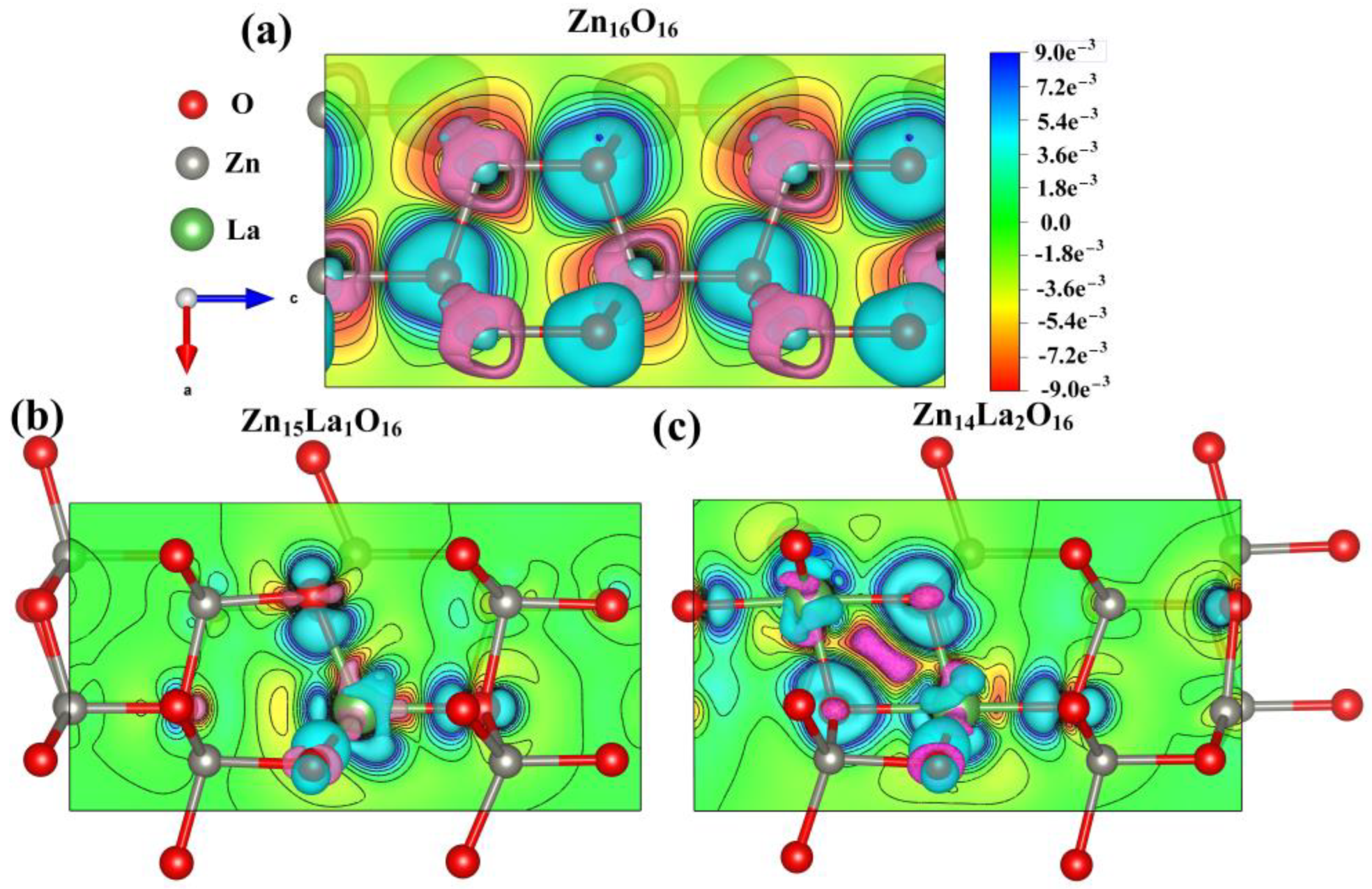
By analyzing the differential charge density diagram of ZnO before and after doping, the bonding between atoms in the La-doped ZnO system can be discussed in a more vivid and intuitive manner [43,44]. The differential charge density distributions of Zn16O16, Zn15La1O16, and Zn14La2O16 on the plane of the doped La atom under spin polarization conditions are calculated, and the calculation results are shown in Figure 4. In the figure, the green electron cloud represents electron aggregation, the pink electron cloud represents electron dissipation, the red color scale bar represents electron gain, and the blue color represents electron loss. The darker the color is, the more electrons are transferred. It can be seen from the analysis that, compared with the electron cloud between the Zn atom and O atom in the intrinsic ZnO system, the doped La atom has a greater impact on the electron cloud density of the surrounding O atom, the interaction is enhanced, and the directivity of the electron cloud is strong. Most of the electrons lost in La are transferred to the O atom. With the increase in the doping concentration of the La atoms, the electron transfer density in the La-O bond area increases, but the overlap of the electron cloud between the La atom and the surrounding O atom in the doped system is weakened. The covalent bond of the doped system is weakened, while the ionic bond of the doped system is strengthened. The calculated results are consistent with the population value, bond length, and stability analysis results of the doped system. These results also can be described by NBO methods, which will be used to further analyze the orbital charge in the future study.

3.7. Optical Properties

The optical properties of semiconductors are closely related to the electronic structure. In the linear response range, the research on the macroscopic optical properties of solids is generally based on the research on the ε ( ω ) = ε 1 ( ω ) + i ε 2 ( ω ) of the complex dielectric function,
ε 1 = n 2 κ 2
ε 2 = 2 n κ
where n is refractive index and κ is extinction coefficient.
Electronic transition includes the in-band transition and inter-band transition of electrons: the in-band transition mainly occurs in metals and the inter-band transition mainly exists in semiconductors. The inter-band transition can be further divided into direct transition and indirect transition. The indirect transition involves phonon dispersion, which has little effect on the dielectric function, so it can be ignored. In this paper, the optical properties of ZnO doped systems are systematically analyzed by calculating its dielectric function, absorption coefficient, reflectivity, and energy loss function. According to the definition of direct transition probability and Kramers–Kronig dispersion relation, the imaginary part ε 2 ( ω ) and real part ε 1 ( ω ) of the crystal dielectric function, absorption coefficient, reflectivity, and energy loss function can be deduced. The specific deduction process will not be repeated [45,46,47].
ε 2 ( ω ) = π ε 0 ( e m ω ) 2 V , C { B Z 2 d K ( 2 π ) 3 | a M V , C | 2 δ [ E C ( K ) E V ( K ) ω ] }
ε 1 ( ω ) = 1 + 2 e ε 0 m 2 V , C B Z 2 d K ( 2 π ) 3 | a M V , C ( K ) | 2 [ E C ( K ) E V ( K ) ] / 1 [ E C ( K ) E V ( K ) ] 2 / 2 ω 2
R ( ω ) = ( n 1 ) 2 + k 2 ( n + 1 ) 2 + k 2
α 2 ω κ c = 4 π κ λ 0
L ( ω ) = Im ( 1 ε ( ω ) ) ε 2 ( ω ) [ ε 1 2 ( ω ) + ε 2 2 ( ω ) ]
where ε 0 is the dielectric constant in vacuum, λ 0 is the wavelength in vacuum, is Planck’s constant, C and V are the conduction band and valence band, respectively, BZ is the first Brillouin zone, K is the electron wave vector, a is the unit direction vector of the vector potential A , M V , C is the transition matrix element, ω is the electromagnetic wave frequency, E C ( K ) and E V ( K ) are the intrinsic energy level on the conduction band and the valence band, respectively, R ( ω ) is the reflectivity, α is the absorption coefficient, and L ( ω ) is the energy loss function.
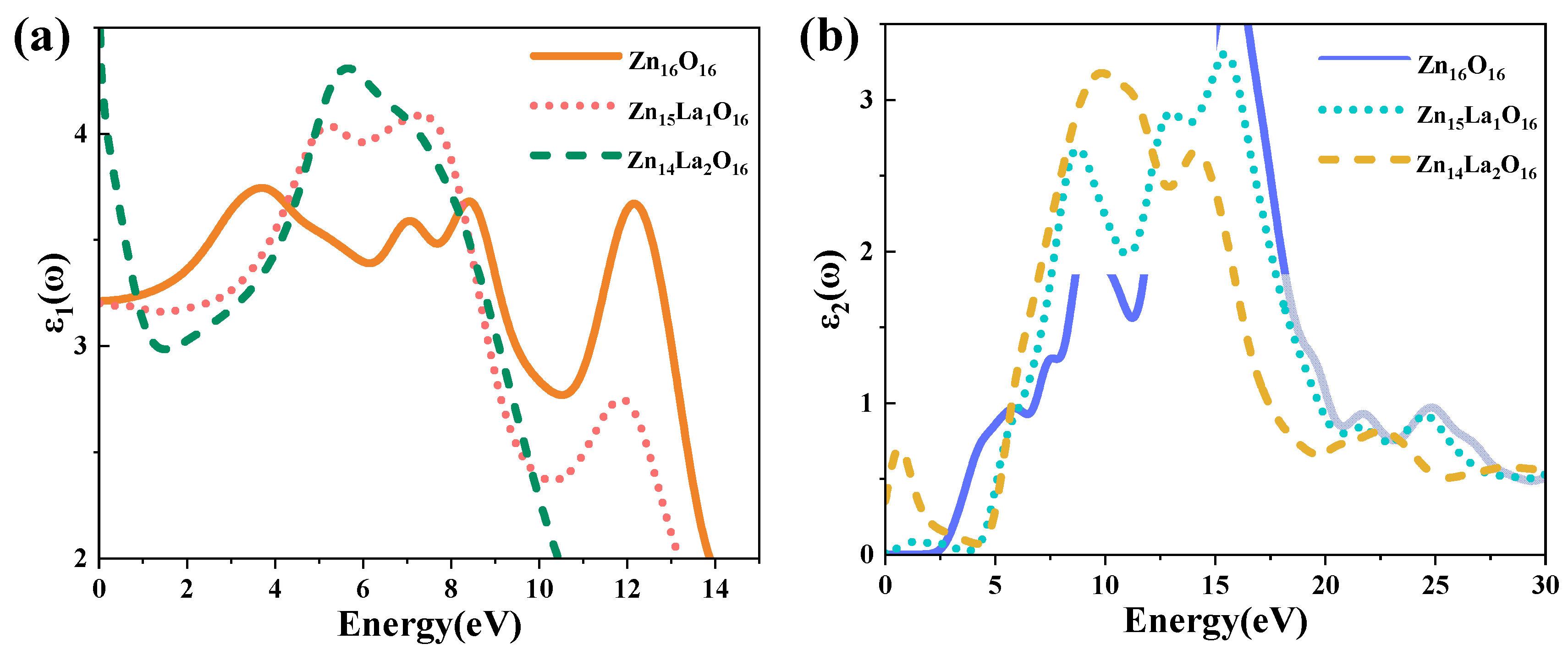
The size of the dielectric constant indicates the capacity of the medium to bind charges. The larger the dielectric constant is, the stronger the capacity of the medium to bind charges is. On the contrary, it means that the binding capacity is weaker [48]. The real part of the dielectric function represents the change in the dielectric constant with the change in photoelectron energy [49], and the imaginary part of the dielectric function reflects the information between the energy band structure and the optical transition. Figure 5 shows the dielectric function curve of the intrinsic ZnO and La-doped ZnO systems. The photoelectron lifetime τ c on the conduction band is proportional to the dielectric constant ε 1 of the photocatalyst. Therefore, the larger the ε 1 of the system, the larger the τ c , that is, the longer the photoelectron lifetime on the conduction band [11]. Figure 5a shows the real part curve of the dielectric function. It can be seen from the analysis that the average static dielectric constant ε 1 a v e ( 0 ) of Zn16O16 is 3.21, and the average static dielectric constant ε 1 a v e ( 0 ) of Zn15La1O16 and Zn14La2O16 is 3.21 and 4.66, respectively. With the increase in the La doping concentration, the dielectric constant of the doped system becomes larger, indicating that La enhances the polarization of the doped system and has strong binding capacity to electrons, that is, it extends the photoelectron lifetime on the conduction band of the doped system and brings good conductivity.
Figure 5b shows the imaginary part curve of the dielectric function. It can be seen from the analysis that the ε 2 ( ω ) of the imaginary part of the dielectric function of the intrinsic ZnO mainly has four peaks: the first dielectric peak is located at 5.82 eV, which is mainly formed by the electronic transition from the top of the valence band to the energy band near the bottom of the conduction band, that is, the transition from the O-2p state at the top of the valence band to the Zn-3p state at the bottom of the conduction band. The second dielectric peak is located at 9.15 eV, which is mainly formed by the complex electronic transitions between the valence band and the top of the valence band away from the Fermi surface, that is, the transition from the Zn-3d state in the valence band to the O-2p state, the transition from the O-2s state in the valence band to the Zn-3d state and other complex electronic transitions. The third dielectric peak is located at 13.33 eV, which is mainly formed by the complex electronic transition between the valence band and the bottom of the conduction band away from the Fermi surface, that is, the transition from the Zn-3d state in the valence band to the Zn-3p state at the bottom of the conduction band. The fourth dielectric peak is located at 15.71 eV, which is mainly formed by the complex electronic transition between the valence band and the bottom of the conduction band away from the Fermi surface, that is, the transition from the O-2s state in the valence band to the Zn-3p state at the bottom of the conduction band. The Zn14La2O16 system has a new peak near 0.67 eV, which is small, and is caused by the in-band transition of La-5d orbital electrons. However, this peak is not found in the imaginary part of the dielectric function of Zn15La1O16 system. In addition, the doping of La affects the O-2s state electrons in the deep valence band region. As a result, with the increase in the doping amount of La, the peak near 9.09 eV moves to the high energy direction and the peak intensity is enhanced, while the peak near 15.71 eV moves to the low energy direction and the peak intensity is weakened.
Figure 6 shows the absorption spectrum and reflection spectrum of the intrinsic ZnO and La-doped ZnO system. Optical absorption is one of the most essential optical properties of ZnO semiconductor materials, reflecting the luminescence mechanism of the spectrum generated by the electronic transition between energy levels. The absorption spectrum calculated according to Formulas (1)–(7) is shown in Figure 6a, with an absorption coefficient of 105 cm−1. Analysis shows that the intensity of the first peak of the doped system is not high, and is generally located in the lower energy range. It is generated due to the electrons that absorb energy and transition from the top of the valence band to the conduction band. Though not obvious, the first peak is crucial. The optical absorption edge of the intrinsic ZnO is around 3.30 eV. The absorption edge is where intrinsic absorption begins to appear and intrinsic absorption determines the key optical properties of ZnO. With the increase in photon energy, the absorption coefficient increases sharply in the order of 105 and strong light absorption occurs, indicating that the direct transition begins. In the visible light region (1.64 eV~3.19 eV), the light absorption edge of Zn15La1O16 and Zn14La2O16 moves towards the direction of high energy, which causes a blue shift. The widening of the optical bandgap Eg because of La atoms introduce a large number of carriers (electrons) as donor atoms, Fermi levels enter the conduction band, resulting in the Burstein–Moss effect. This maximal widening is almost equal to the reported value 0.38 eV resulted from La doping of 0.14 at.%, and larger than the reported value 0.2 and 0.13 eV resulted from La doping of 0.3–0.57 at.% [24]. The optical absorption spectra of Zn15La1O16 and Zn14La2O16 show a smaller new absorption peak near 1.06 eV, which is caused by the in-band transition of La-5d orbit. In the visible light region, compared with the intrinsic ZnO, as the doping concentration of La increases, the absorption spectrum moves to the direction of high energy, resulting in a blue shift, and decreased light absorption intensity. The main absorption peak of Zn16O16 is at 16.96 eV, the main absorption peak of Zn15La1O16 is at 16.60 eV, and the main absorption peak of Zn14La2O16 is at 15.38 eV, which is in the vacuum ultraviolet region. With the increase in La doping concentration, the absorption peak moves to the direction of low energy, resulting in a red shift and a decreased intensity of the main absorption peak. As the doping of La introduces new impurity energy levels, a new emission center is developed, leading to the red shift of ultraviolet emission. These results are the same as the reported conclusion that the light absorption of the films in UV range first blue-shift and then red-shift with the increase in the La content (0.5–2.0 at.%) [30]. The absorption peak mainly comes from the transition of excited state electrons from the valence band to the conduction band. The weakening of the absorption peak intensity indicates that the transition process of electrons in this excited state is reduced after La doping. In addition, the absorption peaks near 25.35 eV, 34.58 eV, and 38.86 eV are red-shifted and weaker than Zn16O16. Therefore, the optical properties of La-doped ZnO become worse in the visible light range, but the light absorption in the ultraviolet region is good, so it can be used as a short wave device.
Reflectivity refers to the macroscopic phenomenon of the electron transition between energy bands in solids under the interference of a photoelectric magnetic field. The reflectivity of intrinsic ZnO and La-doped ZnO systems calculated according to Formulas (1)–(6) is shown in Figure 6b. The static reflectivity R(0) of Zn16O16 is 0.08, and that of Zn15La1O16 and Zn14La2O16 is 0.08 and 0.14. It has high reflectivity in the range of 16 eV to 20 eV. Zn16O16 has maximum reflectivity of 0.24 at 17.2 eV, Zn15La1O16 has maximum reflectivity of 0.28 at 17.8 eV, and Zn14La2O16 has maximum reflectivity of 0.23 at 16.0 eV. In the visible light area, with the increase in the La doping concentration, the reflectivity decreases, which is lower than the intrinsic ZnO. When photons pass through the material, some of them will be reflected, some will be absorbed by the material, and the rest will be transmitted from the material. Therefore, the absorption coefficient and reflectivity of La-doped ZnO decrease both in the visible and ultraviolet regions, thereby resulting in increased transmittance.
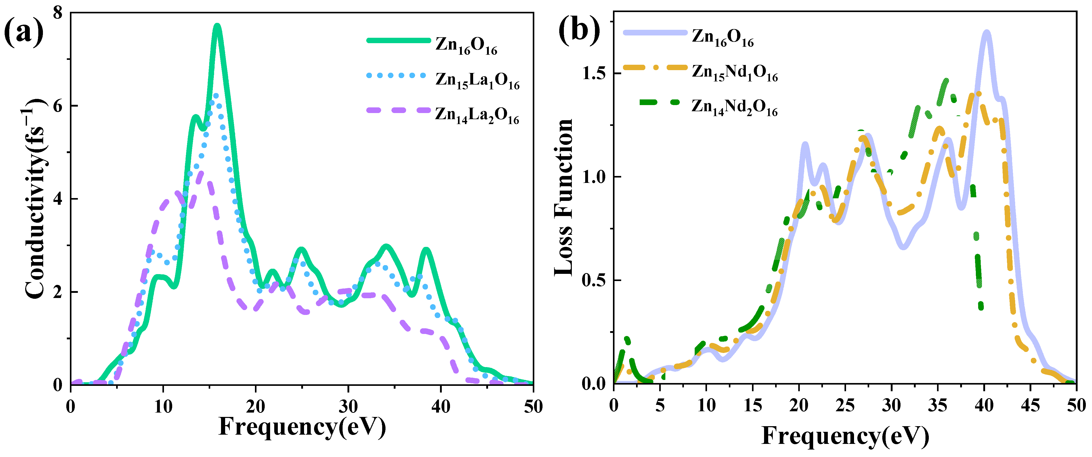
Photoconductivity indicates the change in the conductivity of semiconductor materials along with the light intensity. Figure 7a shows the photoconductivity of intrinsic ZnO and La-doped ZnO systems, which strictly corresponds to the imaginary part ε 2 ( ω ) of the dielectric function (Figure 5b). The analysis shows that the intrinsic ZnO and La-doped ZnO systems have high conductivity, in the range of 10 eV to 20 eV, and the real part reaches its main peak near 15 eV of energy. The peak value of intrinsic ZnO is 7.71 fs−1, and the peak values of Zn15La1O16 and Zn14La2O16 are 6.21 fs−1 and 4.59 fs−1. In the visible light region, the photoconductivity of the intrinsic ZnO and La-doped ZnO systems increases with the increase in the incident photon energy. Compared with the photoconductivity value in the low energy region, it is found that the photoconductivity of the La-doped ZnO system is greater than that of the intrinsic ZnO. This is due to the introduction of excess carriers by the La atom at the Fermi level of the doped system, which increases the photoconductivity in the low energy region, but the photoconductivity of all systems is small. This shows that the doping of La improves the photoconductivity of the ZnO semiconductor in the visible light region.
The energy loss function describes the energy loss of electrons passing through a homogeneous crystal, and its peak value is related to the plasma frequency. Based on calculations with Formulas (1)–(8), the energy loss function reflects the energy loss when photons pass through the crystal. Figure 7b is the energy loss function of the intrinsic ZnO and La-doped ZnO systems. Analysis shows that the plasma frequency of Zn16O16 is 40.29 eV, the plasma frequency of Zn15La1O16 is 38.79 eV, and the plasma frequency of Zn14La2O16 is 18.57 eV. With the increase in the La doping amount, the peak value is red-shifted, and the intensity is always weaker than the intrinsic ZnO system.

3.8. Magnetic Properties

At present, according to the research progress of ZnO thin magnetic semiconductors, the magnetic properties of ZnO semiconductors are induced by intrinsic defects, 3d transition metals, rare-earth elements, and other magnetic ions doping and non-magnetic ions doping. For doping, 3d transition elements (Cr, Mn, Fe, and Co) are the preferred elements due to their unpaired electrons in the 3d shell and large magnetic moment, which can produce strong magnetic properties. A large number of studies have shown that effective transition metal doping can improve the photocatalytic performance of ZnO while presenting room temperature ferromagnetism [28,50,51]. In addition, the optical and magnetic properties of the over metal-doped ZnO system are closely related to the transition metal doping type, preparation environment, and annealing environment. However, the magneto-optical properties of rare-earth-doped ZnO mainly depend on the interaction between the 4f electrons of rare-earth-doped elements and the defects arising from doping in the ZnO body. The magnetic and optical properties of rare-earth doped ZnO have attracted the attention of many researchers [52,53,54]. This paper adopts the spin polarization calculation method. The calculation results output values of 2 * Integrated Spin Density and 2 * Integrated | Spin Density|. The former represents the spin polarization DOS integral results, that is M , the difference between spin-up and spin-down conditions. This result is the Bohr magnetic moment of the system, and 2 is the spin magnetic moment g factor. Whereas, the latter represents the sum of the absolute spin polarization DOS integral, that is | M | , the sum of spin-up and spin-down electron density of state integrals. These two values can be used to preliminarily judge the magnetism of the system. The M = 0 , | M | = 0 of Zn15La1O16 and Zn14La2O16, the total magnetic moment is 0. At the same time, by analyzing the density of states in Figure 3, it is found that the total density of states and the partial wave density of states in the Zn15La1O16 and Zn14La2O16 systems are completely symmetrical in spin-up and spin-down conditions, and the net spin density of states is also a straight line, indicating that the La-doped ZnO system is nonmagnetic. The analysis of the Mullike orbital charge distribution in Table 2 shows that, in the Zn15La1O16 and Zn14La2O16 systems, the spin-up and spin-down orbital electron number of each atom are identical, indicating that the La-doped ZnO system is nonmagnetic, so the La-doped ZnO system has no magnetic moment and no magnetism, which is consistent with the calculation results in study [11], while [55] holds that La-doped ZnO in replacement of Zn is magnetic. The authors of [56] proved that it was due to the existence of Zn vacancies in the doped system.

4. Conclusions

In this paper, based on the density functional theory, the GGA+U method is used to calculate the effect of rare-earth element La doping at different concentrations on the electronic structure, optical properties, and magnetic properties of ZnO under spin polarization conditions. The electronic structure calculation results show that the cell of the La-doped ZnO system is distorted, and the formation energy is less than zero, in which case it is easy to dope. After La doping, the band gap narrows, the Fermi level enters the conduction band, and the excess carriers introduced by La atoms degenerate. The La-doped ZnO system is an n-type degenerate semiconductor, and the carriers enhance the conductivity and metallicity of the system. The calculation results for optical properties show that in the visible light region, the optical absorption edge of the La-doped ZnO system experiences a blue shift, which increases the average static dielectric constant and strengthens the polarization ability and the capacity to bind charges. The photoconductivity of the doped ZnO system is improved. The calculation results on magnetic properties suggest that the magnetic moment of La-doped ZnO system is 0, and the system has no magnetism.

Author Contributions

F.Z. and S.X. supervised the research. Q.W. calculated a series of properties of the material and wrote the first draft. B.Z., G.L., J.N. and T.S. analyzed the data and revised the paper. All authors have read and agreed to the published version of the manuscript.

Funding

This research was funded by the National Natural Science Foundation of China (No.62264015), the National Science Foundation of Shaanxi Province, China (2021JQ-635), Scientific Research Program of Yan’an University (YDQ2020-08) and Scientific and Technological Innovation Team (2017CXTD-01).

Data Availability Statement

All data are presented in the form of charts in the article.

Conflicts of Interest

The authors declare no conflict of interest.

References

  1. Djurisic, A.B.; Ng, A.; Chen, X.Y. ZnO nanostructures for optoelectronics:material properties and device applications. Prog. Quantum Electron. 2010, 34, 191–259. [Google Scholar] [CrossRef]
  2. Tirumalareddygari, S.R.; Guddeti, P.R.; Ramakrishna Reddy, K.T. A critical study of the optical and electrical properties of transparent and conductive Mo-doped ZnO films by adjustment of Mo concentration. Appl. Surf. Sci. 2018, 458, 333–343. [Google Scholar] [CrossRef]
  3. Tay, Y.Y.; Tan, T.T.; Li, S. Determinants of the structured and structureless green emissions of ZnO. Solid State Commun. 2011, 151, 372–376. [Google Scholar] [CrossRef]
  4. Ozgur, U.; Alivov, Y.I.; Liu, C.; Teke, A.; Reshchikov, M.; Dogan, S.; Avrutin, V.; Cho, S.; Morkoc, H. A compre hensive review of ZnO materials and devices. J. Appl. Phys. 2005, 98, 41301. [Google Scholar] [CrossRef]
  5. Santosh, S.; Gupta, K.; Sudarshan, R. Optical nanomaterials with focus on rare earth doped oxide: A Review. Mater. Today Commun. 2021, 27, 102277. [Google Scholar]
  6. Li, H.; Li, W.; Gu, S.; Wang, F.; Zhou, H. In-built Tb4+/Tb3+ redox centers in terbium-doped bismuth molybdate nanograss for enhanced photo catalytic activity. Catal. Sci. Technol. 2016, 6, 3510–3519. [Google Scholar] [CrossRef]
  7. Li, Y.; Wang, R.; Zheng, W.; Li, Y. Silica-coated Ga (III)-doped ZnO: Yb3+, Tm3+ upconver sionnanoparticles for high-resolution in vivo bioimaging using near infrared to near-infrared upconversion emission. Inorg. Chem. 2019, 58, 8230–8236. [Google Scholar] [CrossRef]
  8. Yao, N.; Huang, J.; Fu, K.; Deng, X.; Ding, M.; Xu, X. Rare earth ions doped phosphors for dye-sensitized solar cells applications. RSC Adv. 2016, 6, 17546–17559. [Google Scholar] [CrossRef]
  9. Vettumperumal, R.; Kalyanaraman, S.; Thangavel, R. Optical constants and near infrared emission of Er doped ZnO sol–gel thin films. J. Lumin. 2015, 158, 493–500. [Google Scholar] [CrossRef]
  10. Khuili, M.; Fazouan, N.; Abou El Makarim, H.; Atmani, E.; Rai, D.; Houmad, M. First-principles calculations of rare earth (RE=Tm, Yb, Ce) doped ZnO: Structural, optoelectronic, magnetic, and electrical properties. Vacuum 2020, 181, 109603. [Google Scholar] [CrossRef]
  11. Zhang, X.J.; Mi, B.W.; Wang, X.C.; Bai, H.L. First-principles prediction of electronic structure and magnetic ordering of rare-earth metals doped ZnO. J. Alloys Compd. 2014, 617, 828–833. [Google Scholar] [CrossRef]
  12. Reed, A.E.; Weinstock, R.B.; Weinhold, F. Natural population analysis. J. Chem. Phys. 1985, 83, 735–746. [Google Scholar] [CrossRef]
  13. Segall, M.D.; Shah, R.; Pickard, C.J.; Payne, M. Population analysis in plane wave electronic structure calculations. Mol. Phys. 1996, 89, 571–577. [Google Scholar]
  14. Hirshfeld, F.L. Bonded-atom fragments for describing molecular charge densities. Chim. Acta 1977, 44, 129–138. [Google Scholar] [CrossRef]
  15. Glendening, E.D.; Landis, C.R.; Weinhold, F. Natural bond orbital methods. Wiley Interdiscip. Rev. Comput. Mol. Sci. 2011, 2, 1–42. [Google Scholar] [CrossRef]
  16. Kavitha, E.; Sundaraganesan, N.; Sebastian, S.; Kurt, M. Molecular structure, anharmonic vibrational frequencies and NBO analysis of naphthalene acetic acid by density functional theory calculations. Spectrochim. Acta Part Mol. Biomol. Spectrosc. 2010, 77, 612–619. [Google Scholar] [CrossRef]
  17. James, C.; Raj, A.A.; Reghunathan, R.; Jayakumar, V.S.; Joe, I.H. Structural conformation and vibrational spectroscopic studies of 2,6-bis(p-N,N-dimethyl benzylidene)cyclohexanone using density functional theory. J. Raman Spectrosc. 2006, 37, 1381–1392. [Google Scholar] [CrossRef]
  18. Mouras, R.; Fontana, M.D.; Bourson, P.; Postnikov, A.V. Lattice site of Mg ion in LiNbO3 crystal determined by raman spectroscopy. J. Phys. Condens. Matter 2000, 12, 5053–5059. [Google Scholar] [CrossRef]
  19. Anisimov, V.I.; Zaanen, J.; Andersen, O.K. Band theory and mott insulators: Hubbard U instead of stoner I. Phys. Rev. Condens. Matter 1991, 44, 943–954. [Google Scholar] [CrossRef] [PubMed]
  20. Segall, M.D.; Lindan PJ, D.; Probert, M.J.; Pickard, C.J.; Hasnip, P.J.; Clark, S.J.; Payne, M.C. First-principles simulation: Ideas, illustrations and the CASTEP code. J. Phys. Condens. Matter 2002, 14, 2717–2744. [Google Scholar] [CrossRef]
  21. Freysoldt, C.; Grabowski, B.; Hickel, T.; Neugebauer, J.; Kresse, G.; Janotti, A.; Van de Walle, C.G. First-principles calculations for point defects in solids. Rev. Mod. Phys. 2014, 86, 253–305. [Google Scholar] [CrossRef]
  22. Pham, A.; Assadi, M.H.N.; Yu, A.B.; Li, S. Critical role of Fock exchange in characterizing dopant geometry and magnetic interaction in magnetic semiconductors. Phys. Rev. 2014, 89, 155110. [Google Scholar] [CrossRef]
  23. Cococcioni, M.; de Gironcoli, S. Linear response approach to the calculation of the effective interaction parameters in the LDA+U method. Phys. Rev. 2005, 71, 035105. [Google Scholar] [CrossRef]
  24. Ma, X.; Wu, Y.; Lv, Y. Correlation effects on lattice relaxation and electronic structure of ZnO within the GGA+U formalism. J. Phys. Chem. 2013, 117, 26029–26039. [Google Scholar]
  25. Iyi, N.; Kitamura, K.; Izumi, F.; Yamamoto, J.K.; Hayashi, T.; Asano, H.; Kimura, S. Comparative study of defect structures in lithium niobate with different compositions. J. Solid State Chem. 1992, 101, 340–352. [Google Scholar] [CrossRef]
  26. Li, F.; Zhang, C.; Zhao, M. Magnetic and optical properties of Cu-doped ZnO nanosheet:First-principles calculations. Phys. Low-Dimens. Syst. Nanostr. 2013, 53, 101–105. [Google Scholar] [CrossRef]
  27. Sousa, S.F.; Fernandes, P.A.; Ramos, M.J. General performance of density functionals. J. Phys. Chem. 2007, 111, 10439–10452. [Google Scholar] [CrossRef] [PubMed]
  28. Assadi, M.H.N.; Zhang, Y.B.; Li, S. Predominant role of defects in magnetic interactions in codoped ZnO:Co. J. Phys. Condens. Matter 2010, 22, 296004. [Google Scholar] [CrossRef]
  29. Shakir, M.; Faraz, M.; Sherwani, M.A.; Al-Resayes, S.I. Photocatalytic degradation of the paracetamol drug using lanthanum doped ZnO nanoparticles and their in-vitro cytotoxicity assay. J. Lumin. 2016, 176, 159–167. [Google Scholar] [CrossRef]
  30. He, H.Y.; Huang, J.F.; Fei, J.; Lu, J. La-doping content effect on the optical and electrical properties of La-doped ZnO thin films. J. Mater. Sci. Mater. Electron. 2015, 26, 1205–1211. [Google Scholar] [CrossRef]
  31. Phuruangrat, A.; Dumrongrojthanath, P.; Yayapao, O.; Arin, J.; Thongtem, S.; Thongtem, T. Photocatalytic activity of La-doped ZnO nanostructure materials synthesized by sonochemical method. Rare Met. 2016, 5, 390–395. [Google Scholar] [CrossRef]
  32. Ma, X.; Miao, L.; Bie, S.; Jiang, J. Synergistic effect of V/N-codoped anatase TiO2 photocatalysts. Solid State Commun. 2010, 150, 689–692. [Google Scholar] [CrossRef]
  33. Long, R.; English, N.J. First-principles calculation of nitrogen-tungsten codoping effects on the band structure of anatase-titania. Appl. Phys. Lett. 2009, 94, 132102. [Google Scholar] [CrossRef]
  34. Bomila, R.; Srinivasan, S.; Gunasekaran, S.; Manikandan, A. Enhanced photocatalytic degradation of methylene blue dye, opto-magnetic and antibacterial behaviour of pure and La-doped ZnO nanoparticles. J. Supercond. Nov. Magn. 2018, 31, 855–864. [Google Scholar] [CrossRef]
  35. Lu, J.G.; Fujita, S.; Kawaharamura, T.; Nishinaka, H.; Kamada, Y.; Ohshima, T.; Ye, Z.Z.; Zeng, Y.J.; Zhang, Y.Z.; Zhu, L.P. Carrier concentration dependence of band gap shift in n-type ZnO: Al films. J. Appl. Phys. 2007, 101, 083705. [Google Scholar] [CrossRef]
  36. Schleife, A.; Rodl, C.; Fuchs, F.; Furthmueller, J.; Bechstedt, F. Optical and energy-loss spectra of MgO, ZnO, and CdO from ab initio many-body calculations. Phys. Rev. 2009, 80, 035112. [Google Scholar] [CrossRef]
  37. Li, H.; Lv, Y.; Li, J.; Yu, K. Experimental and first-principles studies of structural and optical properties of rare earth (RE=La, Er, Nd) doped ZnO. J. Alloys Compd. 2014, 617, 102–107. [Google Scholar]
  38. Hu, Y.; Zeng, H.; Du, J.; Hu, Z.; Zhang, S. The structural, electrical and optical properties of Mg-doped ZnO with differrent interstitial Mg concentration. Mater. Chem. Phys. 2016, 182, 15–21. [Google Scholar] [CrossRef]
  39. Zhang, L. First-Principles Study on the Electronic Structure and Optical Properties of La-Doped ZnO; North University of China: Shanxi, China, 2021. [Google Scholar]
  40. Xu, G.X. Quantum Chemistry Secondary Volume; Science Press: Beijing, China, 2022. (In Chinese) [Google Scholar]
  41. Sun, C.Q. Oxidation Electronics: Bond-Band-Barrier correlation and its applications. Prog. Mater. Sci. 2003, 48, 521–685. [Google Scholar] [CrossRef]
  42. Segall, M.D.; Pickard, C.J.; Shah, R.; Payne, M.C. Population analysis in plane-wave electronic structure calculations of bulk materials. Phys. Rev. 1996, 54, 16317–16320. [Google Scholar] [CrossRef]
  43. Wu, H.C.; Chen, H.H.; Zhu, Y.R. Effects of Al-impurity type on formation energy, crystal structure, electronic structure, and optical properties of ZnO by using density functional theory and the hubbard-U method. Materials 2016, 9, 647. [Google Scholar] [PubMed]
  44. Sha, S.L. First-Principles Study of Effect of Different Valence States Mo-Doping and Point Defect on the Magnetic and Optical Properties of ZnO; Inner Mongolia University of Technology: Hohhot, China, 2021. [Google Scholar]
  45. Huang, K. Solid Physics; Higher Education Press: Beijing, China, 2002. (In Chinese) [Google Scholar]
  46. Fang, R.C. Solid State Spectroscopy; University of Science and Technology of China Press: Hefei, China, 2001. (In Chinese) [Google Scholar]
  47. Shen, X.C. Spectra and Optical Properties of Semiconductors, 2nd ed.; Science Press: Beijing, China, 2002. (In Chinese) [Google Scholar]
  48. Yang, R.Y.; Yan, H.X.; Xiao, Y.; Guo, Z.H. The optical properties of one-dimensional ZnO: A first-principles study. Chem. Phys. Lett. 2007, 446, 98–102. [Google Scholar] [CrossRef]
  49. Zhang, X.D.; Guo, M.L.; Li, W.X.; Liu, C.L. First-principles study of electronic and optical properties in wurtzite Zn1−xCdxO. J. Appl. Phys. 2008, 103, 063721. [Google Scholar]
  50. Yoon, D.H.; Muksin, K.; Raju, S. Structural, and magnetic properties of Co-doped and Mn-doped ZnO nanocrystalline DMS prepared by the facile polyvinyl alcohol gel method. J. Supercond. Nov. Magn. 2017, 30, 203–208. [Google Scholar] [CrossRef]
  51. Liu, H.; Zhang, J.M. Effect of two identical 3d transition-metal atoms M doping (M=V, Cr, Mn, Fe, Co, and Ni) on the structural, electronic, and magnetic properties of ZnO. Phys. Status Solidi B-Basic Solid State Phys. 2017, 254, 1700098. [Google Scholar] [CrossRef]
  52. Zamiri, R.; Lemos, A.F.; Reblo, A.; Ahangar, H.A.; Ferreira, J.M.F. Effects of rare-earth (Er, La and Yb) doping on morphology and structure properties of ZnO nanostructures prepared by wet chemical method. Ceram. Int. 2014, 40, 523–529. [Google Scholar] [CrossRef]
  53. Ali, D.; Butt, M.Z.; Muneer, I. Synthesis and characterization of sol-gel derived La and Sm doped ZnO thin films: A solar light photocatalyst for methylene blue. Thin Solid Film 2019, 679, 86–98. [Google Scholar] [CrossRef]
  54. Asikuzun, E.; Ozturk, O.; Arda, L.; Tasci, A.T.; Kartal, F.; Terzioglu, C. High-quality C-axis oriented non-vacuum Er doped ZnO thin films. Ceram. Int. 2016, 42, 8085–8091. [Google Scholar] [CrossRef]
  55. Young, S.L.; Chen, H.Z.; Kao, M.C.; Kung, C.Y.; Lin, C.C.; Lin, T.T.; Horng, L.; Shih, Y.T.; Ou, C.J.; Lin, C.H. Magnetic properties of La-doped and Cu-doped ZnO nanowires fabricated by hyderothermal method. Int. J. Mod. Phys. 2013, 27, 1362006. [Google Scholar] [CrossRef]
  56. Li, W.L. Effect of La/Cu-Doping and Point Defect on the Magnetic and Optical Properties of ZnO by First-Principle; Inner Mongol University of Technology: Hohhot, China, 2019. [Google Scholar]
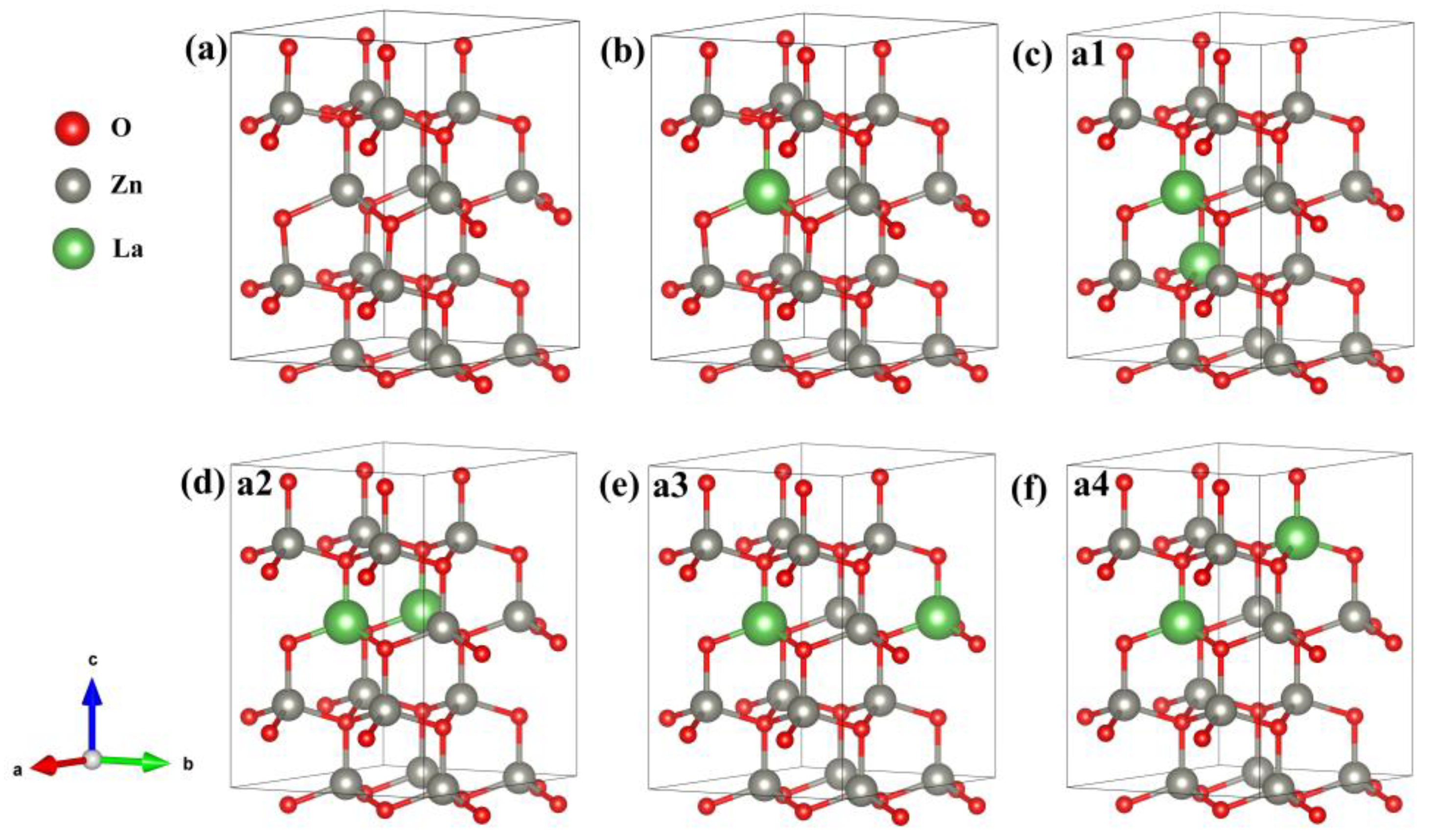
Figure 1. Calculation model. (a) Zn16O16, (b) Zn15La1O16, (c) Zn14La2O16a1, (d) Zn14La2O16a2, (e) Zn14La2O16a3, (f) Zn14La2O16a4. Annotation: a1–a4 represents four different configurations for Zn14La2O16.
Crystals 13 00754 g001
Figure 2. Energy band structure near Fermi surface. (a) Zn16O16, (b) Zn15La1O16, (c) Zn14La2O16. Annotation: The red lines representative spin up and the blue lines representative spin down.
Crystals 13 00754 g002
Figure 3. Density of state. (a) Zn16O16, (b) Zn15La1O16, (c) Zn14La2O16.
Crystals 13 00754 g003
Figure 4. Differential charge density diagram. (a) Zn16O16, (b) Zn15La1O16, (c) Zn14La2O16.
Crystals 13 00754 g004
Figure 5. Dielectric function. (a) Real part of dielectric function, (b) imaginary part of dielectric function.
Crystals 13 00754 g005
Figure 6. (a) Absorption spectrum, (b) Reflectivity.
Crystals 13 00754 g006
Figure 7. (a) Photoconductivity, (b) Energy loss function.
Crystals 13 00754 g007
Table 1. Cell parameters and formation energy after structural optimization of intrinsic ZnO and La-doped ZnO systems.
Modela/Åb/Åc/ÅαβγV/Å3Ef/eV
Zn16O166.8216.82110.94290.00°90.00°120.00°440.898-
Zn15La1O166.9096.90910.97990.00°90.00°119.99°453.885−6.505
Zn14La2O16a17.0567.06410.75890.00°89.89°120.01°464.264−12.519
Zn14La2O16a27.2327.09010.45990.06°90.02°120.64°461.378−11.962
Zn14La2O16a37.0917.09110.45789.93°90.07°118.65°461.387−11.956
Zn14La2O16a47.0967.09610.56889.99°89.99°119.97°460.942−12.496
Annotation: a1–a4 represents four different configurations for Zn14La2O16.
Table 2. Mulliken charge distribution of intrinsic ZnO and La-doped ZnO systems.
ModelAtomspdTotal
/eV
Net Charge/e
Zn16O16Zn (spin up)0.200.344.995.540.93
Zn (spin down)0.200.344.995.54-
O (spin up)0.922.550.003.46−0.93
O (spin down)0.922.550.003.46-
Zn15La1O16Zn (spin up)0.190.364.995.540.93
Zn (spin down)0.190.364.995.54-
O (spin up)0.912.560.003.47−0.95
O (spin down)0.912.560.003.47-
La (spin up)0.15−0.220.680.621.77
La (spin down)0.15−0.220.680.62-
Zn14La2O16Zn (spin up)0.260.365.005.620.76
Zn (spin down)0.260.365.005.62-
O (spin up)0.932.530.003.46−0.92
O (spin down)0.932.530.003.46-
La (spin up)0.25−0.170.710.791.42
La (spin down)0.25−0.170.710.79-
Table 3. Population value and bond length of inherent ZnO and La-doped ZnO system.
ModelBond TypePopulation ValueBond Length
Zn16O16Zn-Omax1.081.966
Zn-Omin0.121.975
Zn15La1O16Zn-Omax0.322.052
Zn-Omin0.411.966
La-O (//c)0.272.313
La-O (⊥c)0.32.264
Zn14La2O16Zn-Omax0.252.166
Zn-Omin0.392.050
La-O (//c)0.272.303
La-O (⊥c)0.182.376
Disclaimer/Publisher’s Note: The statements, opinions and data contained in all publications are solely those of the individual author(s) and contributor(s) and not of MDPI and/or the editor(s). MDPI and/or the editor(s) disclaim responsibility for any injury to people or property resulting from any ideas, methods, instructions or products referred to in the content.