Abstract
Zr/Nb nanoscale multilayers are regarded as one of the important candidate materials used in next-generation reactors. Understanding structural evolution induced by ion bombardment is crucial for the evaluation of lifetime performance. Magnetron sputter-deposited Zr/Nb multilayers with a periodicity of 7 nm were subjected to 300 keV He ion irradiation with three different fluences at room temperature. The depth-resolved strain and damage profiles in the Zr/Nb multilayers were investigated by grazing incidence X-ray diffraction. The tensile strain was found in the deposited Zr/Nb films. After He ion irradiation, the intensity of diffraction peaks increased. The change in diffraction peaks depends on He fluence and incident angle. Irradiation-induced pre-existing defect annealing was observed and the ability to recover the microstructure was more significant in the Zr films compared to the Nb films. Furthermore, the efficiency of defect annealing depends on the concentration of pre-existing defects and He fluence. When the He fluence exceeds the one for pre-existing defect annealing, residual defects will be formed, such as 1/3<110> and 1/3<100> dislocation loops in the Zr films and 1/2<111> dislocation loops in the Nb films. Finally, introducing deposited defects and interfaces can improve the radiation resistance of Zr/Nb nanoscale multilayers. These findings can be extended to other multilayers in order to develop candidate materials for fusion and fission systems with high radiation resistance.
1. Introduction
In advanced Gen-IV nuclear reactors, structural materials suffer from being exposed to extreme environments, such as high temperatures of up to 800 °C and intense neutron irradiation of more than 100 dpa (displacements per atom). Moreover, substantial production of helium atoms via (n, α) transmutation reactions is typical in some fission systems. Helium concentration is very high in structural materials. Due to the very low solubility of He in metals, helium atoms preferentially occupy high excess volume sites like grain boundaries and vacancy clusters. In this case, high-temperature He embrittlement and swelling become increasingly serious [1,2]. Traditional structural materials used in light-water reactors, i.e., austenitic steels, cannot satisfy future demands. In order to improve the irradiation resistance and thermal stability of these alloys, increasing grain boundaries and heterointerfaces that play the role of an effective sink for irradiation-induced point defects to encourage vacancy-interstitial recombination are widely employed [3,4,5,6]. In addition, Demkowicz et al. [7] reported He outgassing via interfaces of Cu-Nb multilayers, so He-induced degradation would be delayed. Based on this concept of enhancing tolerance to radiation damage during He and neutron bombardment, nanolayered laminates have been fabricated for decades [8,9,10,11,12,13,14,15,16]. Sputter-deposited nanoscale metallic multilayers have been widely investigated to study interfaces with a variety of orientations, thicknesses and chemical elements, such as FCC/FCC multilayers (Cu/Co [8], Cu/Ag [9] and Ag/Ni [10]), FCC/BCC multilayers (Cu/V [11], Cu/Nb [12], Cu/W [13] and Ag/V [14]), BCC/BCC multilayers (Fe/W [15]) and BCC/HCP multilayers (Nb/Zr [16]). Concerning the proposed limits for neutron-induced radioactivity and lattice swelling, only a few FCC metals are able to applicate in advanced Gen-IV nuclear reactors. So far, Zr-based alloys have acted as fuel cladding materials used in the present light-water nuclear reactors [17,18,19]. Zhang et al. argued that immiscible systems generally possess good radiation tolerance because of their high sink capability and stable interfacial structure under irradiation [6]. Zr/Nb is an immiscible system with a positive heat of mixing of +6 kJ mol−1 at equiatomic concentration [20], so Zr/Nb multilayers are considered promising candidate materials for fuel cladding applications to improve irradiation resistance in the light-water nuclear reactors. It is worth investigating radiation damage of Zr/Nb multilayers.
Irradiation damage behavior in Zr/Nb multilayers has been widely studied in the past. Callisti et al. [21] studied γ-irradiated Zr/Nb multilayer film with bi-layer periods of 10, 30 and 60 nm to a dose of 510 kGy. The increase in hardness to 0.35 GPa was found for the smallest periodicity, with similar hardening effects of Cu-irradiated Zr/Nb nanoscale multilayers (6 and 27 nm). The layered structure kept stable under ion irradiation, except for forming amorphous clusters at the interphase boundary. Liang et al. [22] used He-irradiated Zr/Nb nanoscale multilayers at room temperature, and found a softening behavior at 1 × 10¹⁷ ions/cm2 with the bi-layer thickness of 5 nm due to radiation-induced amorphization near the interface and bubble chains formed on the interphase boundary. Daghbouj et al. [20] investigated interphase boundary layer-dominated strains in Cu-irradiated Zr/Nb nanoscale multilayers. A tensile strain long c-axis in Nb layer and a compressive strain in Zr layer when the bi-layer thickness is 27 nm, while a compressive strain in both layers for the thick multilayer (96 nm). In the vicinity of the interface on the Zr side, Frankel pairs exhibit high mobility compared to the Nb side, so less lattice defects are visible on the Zr side. Furthermore, Daghbouj et al. [23] studied C, Si, Cu-irradiated Zr/Nb nanoscale multilayers with the bi-layer thicknesses of 6, 27 and 96 nm, and they found that irradiation hardening in the thin nanoscale multilayers was minuscule (maximum 8%), but found a significant hardening in the thick ones (maximum 24%). No softening phenomenon was observed after ion irradiation. Furthermore, they argued that the change in strain in the irradiation hardening was independent of the type of irradiated ions (C, Si and Cu). In addition to radiation hardening and irradiation-induced defects, the stability of nanofilms after ion irradiation was also reported. Radhakrishnan et al. [24] observed layer dissolution behavior in accumulative roll bonded bulk Zr/Nb nanoscale multilayers under Zr irradiation at 500 °C. This phenomenon is caused by the liquid phase miscibility within thermal spikes. General speaking, the strengthening mechanisms of nanoscale multilayers are accounted for in the Hall-Patch (H-P) model (dislocation pile-ups), the confined layer slip (CLS) model (Orowan bowing of single dislocation) and the interface barrier strength (IBS) model (dislocation location cutting through an interface) [25,26]. Radiation-induced interphase mixing and amorphization usually result in softening behavior. In addition, the irradiation-induced lattice strain also affects the hardness change of multilayers. For example, Zare et al. [27] investigated Fe/SiOC nanolaminate films after Fe ion irradiation, and found an increase in the compressive residual stress and hardness in the Fe films. There is a linear relationship between the irradiation-induced increase in the hardness of the Fe films and increasing compressive residual stress. As we know, due to the different crystal structures and lattice constants (a = b = 323.2 pm, c = 514.7 pm for Zr and a = b = c = 330.04 pm for Nb) between Zr and Nb, there are amounts of deposited defects at the interface of films. These defects in the as-deposited multilayers can affect the evolution of structural damage after ion irradiation. The annealing behaviors of nano-scaled multilayers, such as Gd/Co, Ni/Zr, Ag/Cu, Al/Ti, etc., have been widely reported [28,29,30,31]. In general, the annealing of crystalline multilayers composed of two miscible elements causes interfacial mixing, to form binary alloys at the interfaces. For example, intermetallic GdCo2 alloy was formed by annealing Gd/Co multilayers at 600 °C for 0.5 h [28]. An amorphous mixed layer was formed at the Ni-on-Zr interfaces for the Ni/Zr multilayers annealed at 400 °C [29]. In addition, Huo et al. [30] reported that the strength and electrical conductivity in Ag/Cu multilayers were improved by annealing at 200–400 °C. A similar phenomenon of annealing-induced hardening in Al/Ti multilayers was reported by Zhang et al. [31]. The findings of irradiation-induced defect annealing have been widely reported in many materials. How about ion irradiation of nanoscale multilayers? To date, there have been less reports of pre-existing defect annealing in the nanoscale multilayers. How about the interaction between deposited defects and irradiation-induced defects? X-ray diffraction is a widely used instrument for characterizing crystalline structures [32,33,34,35]. Due to limited penetration depth and heterogeneous damage distribution of ion irradiation, the depth distribution of lattice structures measured by grazing incidence X-ray diffraction is a common method. Huang et al. [36] investigated structural evolution in low-energy and high-fluence He-implanted pure W by using synchrotron grazing incidence X-ray diffraction (S-GIXRD). The un-implanted W surface layer was composed of the compressed zone and the unaffected matrix. After He implantation, the W surface layer was composed of four zones from the sample surface to deep depth: the compressed zone, transition zone, expanded zone and the matrix, which are determined by adjusting the incident angle of the X-ray. Therefore, variations in the lattice parameter and structure can be accurately measured by GIXRD. The radiation resistance of Zr/Nb multilayers depends on the individual thickness [23]. Thin Zr/Nb multilayers exhibit higher radiation resistance due to the interfaces acting as an efficient sink for defect recombination. Therefore, it is worth studying thin Zr/Nb multilayers, which are a more promising candidate for the cladding of fuel rods compared to the thick ones.
In this study, Zr/Nb nanoscale multilayers with a periodicity of 3/4 nm were fabricated by the magnetron sputtering method. We used 300 keV He ions with fluences of 2 × 10¹⁶ ions/cm2, 5 × 10¹⁶ ions/cm2 and 1 × 10¹⁷ ions/cm2 at room temperature for irradiation experiments. The structural evolution after different irradiation fluences was investigated by GIXRD. This work sheds light on the radiation behavior of Zr/Nb nanoscale multilayers.
2. Experiment Process
The Zr/Nb nanoscale multilayers were fabricated by magnetron sputtering (magnetron sputtering machine produced by Beijing Technol Science Co., Ltd.). High purity argon (99.999%) gas was used as the sputtering gas. A metallic Zr target of high purity (99.95%) and a Nb target of high purity (99.99%) were utilized to deposit the Zr/Nb nanoscale multilayers. The base pressure was about 10−5 Pa. The working pressure of the Ar gas was set at 0.5 Pa, while the rate of Ar flow was 10 standard cubic centimeters per minute (SCCM). The films had a total thickness of ~1 μm and were deposited on a Si wafer at 573 K substrate temperature and −250 V DC substrate bias.
The as-deposited films were irradiated with 300 keV He2+ ions to fluences of 2 × 10¹⁶ ions/cm2, 5 × 10¹⁶ ions/cm2 and 1 × 10¹⁷ ions/cm2 at room temperature. The beam flux was maintained in the order of 1013 ions/cm2s. The increase in sample temperature ΔT during ion irradiation can be estimated by the following equation [37]:
where J is beam power density in units of W/cm2, kT is thermal conductance in units of W/cm. K, t is irradiation time, ρ is the density of material in units of g/cm3 and CT is specific heat in units of J/g·K. According to Equation (1) and the present experimental condition, ΔT can be calculated to be 47 °C, 74.5 °C and 105 °C after He ion irradiation with a irradiation fluence of 2 × 10¹⁶ ions/cm2, 5 × 10¹⁶ ions/cm2 and 1 × 10¹⁷ ions/cm2, respectively. The He2+ ion irradiation was carried out on a 320 kV high-voltage platform at the Institute of Modern Physics, Chinese Academy of Sciences. In order to provide uniform ion fluence across the sample, the beam was scanned by changing electron field polarity. The sample size was 10 × 10 × 0.4 mm3 and the beam size was 16 × 17 cm2, so the whole sample surface was irradiated by the beam. Depth profiles of the He irradiation-induced displacement damage and the implanted helium were simulated by the Monte-Carlo code Stopping and Range of Ions in Matter (SRIM-2013) quick cascade simulations using a displacement energy of 40 eV and a density of 7.68 g/cm3 [38]. As shown in Figure 1, the ion projected range was 734 ± 135.7 nm, which was within the Zr/Nb multilayers.
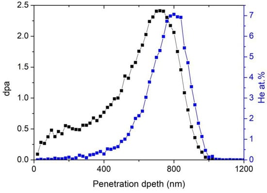
Figure 1.
Depth profiles of the displacement damage in dpa and the helium atom deposition in at.% of 300 keV He irradiation to a fluence of 1 × 10¹⁷ ions/cm2.
Due to the limited penetration depth of He ions in the Zr/Nb multilayers, the structural change with different depths was measured by grazing incidence X-ray diffraction (GIXRD) using a PANalytical (Netherlands) X-ray diffractometer with Cu Kα radiation, and θ–2θ geometry. The incident angles were 1°, 2°, 3°and 4°. The step size of the scan angle was 0.02°. The measured depth corresponding to different incident angles in the GIXRD test was estimated by a critical angle model following Equations [39].
where γc is the critical angle, ρ is the material density, λ is the wavelength of X-ray in Å, d is the measured depth, γ is the incident angle and μ is the linear attenuation coefficient. In this study, the ρ is 7.68 g·cm−3, λ is 1.5406 Å and μ is estimated to 1067 cm−1 (depending on the quality of the film), so the γc is 0.391°. When γ < γc, the measured depth is calculated by Equation (3), while the measured depth is calculated by Equation (4) when γ > γc. The penetration depths of the reflecting X-ray in Zr/Nb multilayers at the incident angle of 1°, 2°, 3° and 4° could be determined as 218, 654, 981 and 1308 nm, respectively. The microstructure of the as-deposited multilayers was checked by transmission electron microscopy using a Tecnai G20 operated at 200 kV with a point resolution of 0.19 nm. Finally, a cross-sectional transmission electron microscopy (XTEM) sample was prepared by mechanical polishing and Ar ion milling. Elemental distribution was measured by energy dispersive spectrometry (EDS).
γc = 1.6 × 10⁻³ ρ1/2λ
3. Results and Discussion
The microstructure of the as-deposited Zr/Nb multilayers is presented in Figure 2. It can be seen that the total thickness of the deposited film is 1 μm (see Figure 2a). The EDS profile of Zr and Nb films in Figure 2b that were alternatively deposited. The high-resolution TEM image in Figure 2c presents the Zr layer exhibiting bright contrast with a thickness of 3 nm and Nb layer exhibiting dark contrast with a thickness of 4.3 nm. The selected area electron diffraction pattern shows single crystalline Zr and Nb films, as shown in the inset of Figure 2c. It should be noted that the interface between Zr and Nb layers is not well distinguished. There is an interfacial transition zone (ITZ) with a thickness of 0.6 nm, where Nb atoms were dissolved into Zr matrix. Black mottle contrasts originated from lattice defects (i.e., interface defects, stacking faults and defect clusters) that were visible in the Zr and Nb layers.

Figure 2.
XTEM bright-filed micrographs showing (a) the over-viewed distribution of the deposited Zr/Nb multilayers, (b) magnified Zr/Nb multilayers and linear scan of Zr and Nb elements, (c) high-resolution TEM of Zr/Nb multilayers and the fast Fourier transform (FFT) pattern showing [011]Zr // [011]Nb, (d) an interfacial transition zone with 0.6 nm and mottled contrasts observed in the Zr and Nb layers.
Although the diffraction intensity was not strong, the grazing incidence X-ray diffraction pattern still presented two diffraction peaks, corresponding to (20)Zr and (211)Nb planes, as shown in Figure 3. It should be noted that the theoretical value of (20)Zr is 63.823°, while the measured value is 63.699° for 1° incidence. Similarly, the theoretical value of (211)Nb is 69.585°, while the measured value is 69.289°, indicating tensile strain caused by deposited defects in the as-fabricated films. The peak position shifted to higher angles with increasing incident angle, and gradually arrived at the real one. This finding demonstrates that lattice strain increased with increasing the thickness of the as-deposited films. For the Zr films, the peak position is 63.699° at an incident angle of 1°, and it is 63.792°at an incident angle of 4°. However, for the Nb films, it is 69.289° at the incident angle of 1°, and it is 69.587° at the incident angle of 4°. The change in Bragg angle of Zr films at 1° to 4° is only 0.093°, while it is 0.298° for the Nb films. This finding demonstrates that tensile strain is more significant in the Nb films than that in the Zr films. It can be seen that the intensity of diffraction peaks increased with increasing incident angle. An incident X-ray with an intensity of I0 enters into a thin film from the surface to a distance d at an incident angle ω. The intensity of the diffraction X-ray can be expressed as [40]:
where dω, ω, 2θ, μ and ρ are the penetration depth of X-ray, incident angle, Bragg angle, linear absorption coefficient of the X-ray and the density of the sample, respectively. The intensity of X-ray increases with increasing incident angle, while the increasing magnitude of X-ray gradually decreases with increasing incident angle.

Figure 3.
The as-deposited Zr/Nb nanoscale multilayers measured by grazing incidence X-ray diffraction (incident angle: 1°, 2°, 3°and 4°).
Interestingly, the increase in intensity of diffraction peaks with increasing incident angle is different. Alternatively, the signal of (211)Nb diffraction peak increased more significantly than that of (20)Zr. In the present experiment, the grazing incident angles were 1°, 2°, 3°and 4°. According to Equation (3), the ideal penetration depths were 218, 654, 981 and 1308 nm. However, there are amounts of lattice defects in the deposited films (see Figure 2d). Those defects can absorp the incident light, decreasing X-ray penetration depth. Therefore, the real measured depth is smaller than the ideal value. The relative intensity of the diffraction X-ray can be written down as [41]:
where P is the multiplicity factor, FHKL is the structural factor, is the angular factor, A(ϴ) is absorption factor, e−2M is temperature factor. It can be seen that there are five different parameters which can affect the intensity of the diffraction X-ray. However, in the present condition, we consider the absorption factor to play the most important role in the change of the diffraction X-ray. As shown in Figure 1b,d, compared to Zr films, more black-mottled contrasts in the Nb were observed. Furthermore, the rapid increase in the intensity of diffraction X-ray with an increasing incident angle for (211)Nb demonstrated that structural defects in Nb films were heterogeneously distributed. Compared to the interior of the film, disordered Nb atoms were preferentially generated in the near-surface region. On the contrary, fewer structural defects were formed in the Zr films, consistent with the results of Daghbouj et al. [23], who found that the lattice strain in the as-deposited Zr layers was smaller than that of the Nb layers.
After He ion irradiation, structural damage was measured by grazing incidence X-ray diffraction, as shown in Figure 4. It can be seen that the intensities of both diffraction peaks increased after He ion irradiation. Furthermore, an asymmetric broadening of the (211)Nb diffraction peak after He ion irradiation was observed. On the left of the (211)Nb diffraction peak, a broad peak was located at about 67.4°, indicating a tensile strain of 2.85% formed inside the Nb films. Note that the change of (20)Zr and (211)Nb is different with the incident angle. Using the Gauss function, we fitted the diffraction peaks of (20)Zr and (211)Nb. The integral intensity, peak position and full-width at half maximum (FWHM) for each fluence and incident angle were determined by simultaneously fitting the pattern with the standard deviation that depends on the shape of diffraction peaks. The detailed values are given in Table 1.

Figure 4.
Grazing incidence X-ray diffraction patterns of (2 0)Zr and (211)Nb before and after He ion irradiation to fluences of 2 × 10¹⁶ ions/cm2, 5 × 10¹⁶ ions/cm2 and 1 × 10¹⁷ ions/cm2 observed under different incident angles: (a) 1°, (b) 2°, (c) 3° and (d) 4°.

Table 1.
The values of area, FWHM and peak with the standard deviation at different incident angles.
The values of the area, full-width at half maximum (FWHM) and peak position are presented in Figure 5. For the change in the (20)Zr diffraction peak, the area increased with increasing fluence at 1° and 2°, and reached the maximum at a fluence of 5 × 10¹⁶ ions/cm2. However, the area was the maximum at a fluence of 2 × 10¹⁶ ions/cm2. The profiles initially increased, then decreased, and finally increased again with increasing fluence at 3° and 4°. The FWHM slightly increased at 2 × 10¹⁶ ions/cm2 and then decreased with increasing fluence. The value of FWHM was smaller than that of the as-deposited sample at 2°, 3° and 4°, but not at 1°. Similarly, the peak position shifted to lower angles with increasing fluence at 1° and 2°, while it initially increased and then decreased with increasing fluence at 3° and 4°. At the fluence of 1 × 10¹⁷ ions/cm2, the peak position was smaller than that of the deposited sample, indicating a tensile strain of 0.28% in the Zr film.
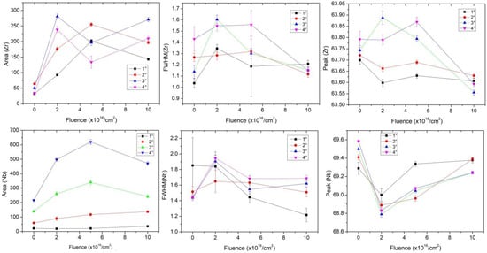
Figure 5.
The change in area, peak position and FWHM of (2 0)Zr and (211)Nb diffraction peaks with He fluence.
For the change in the (211)Nb diffraction peak, the area slightly increased with increasing fluence at 1° and 2°, while it obviously increased at 3° and 4°. The FWHM decreased with increasing fluence at 1°, while it initially increased and then decreased with increasing fluence at 2°, 3° and 4°. At the fluence of 1 × 10¹⁷ ions/cm2, the value of FWHM was larger than that of the as-deposited sample at 3° and 4°. The peak position initially shifted to lower angles and then to higher angles with increasing fluence. At the fluence of 1 × 10¹⁷ ions/cm2, the peak position was almost the same as the as-deposited sample at 1° and 2°, while it was slightly smaller than that of the as-deposited sample at 3° and 4°, indicating the increase in tensile strain after He ion irradiation.
Based on the abovementioned results, it was the same change that the intensities of (20)Zr and (211)Nb diffraction peaks increased after He ion irradiation. However, the increasing magnitude of (20)Zr was larger than (211)Nb. Irradiation-induced defect annealing has been reported in many materials [42,43,44,45,46]. For example, Han et al. reported H-ion irradiation-induced annealing in He-ion-implanted 4H-SiC by measuring the change in Raman intensity [42]. The efficiency of defect annealing is related to the concentration of pre-existing defects formed by He implantation. The annealing level decreases with increasing pre-existing defects. It is hard to heal an amorphous SiC via ion irradiation [39]. Similarly, Heera et al. [45] investigated the recrystallization behavior of amorphous 6H-SiC caused by implantation with 200 keV Ge+. They found the recrystallization of 6H-SiC utilizing 300 keV Si+ ion irradiation and subsequent low-temperature annealing. Jiang et al. [46] found Ni grain growth in amorphous ZrC/nanocrystalline Ni multilayers after He ion irradiation at room temperature. Ferre et al. [47] reported the amorphous-to-crystalline transformation and grain growth of nanocrystalline Al2O3 after W and Au ion irradiation at 600 °C. Irradiation-induced grain growth is a general phenomenon. The grain growth kinetics depend on ion energy and temperature. Irradiation-enhanced defect diffusion can explain the present experimental results. Daghbouj et al. [48] calculated the migration energy barriers for the point defects in Zr rand Nb single crystals by density-functional theory (DFT). The energy barriers for self-interstitial atoms (SIAs, 0.4 eV in Zr and 0.5 eV in Nb), and vacancies (0.6 eV in Zr and 2.25 eV in Nb) were obtained. The lower energy barriers indicated that the mobility of defects is higher in the Zr layers than in the Nb layers. Therefore, the irradiation-induced defect annealing is more significant in Zr layers compared to Nb layers. It can explain the rapid increase in the intensity of the (20)Zr diffraction peak after He ion irradiation. The ability of irradiation-induced defect annealing depends on the concentration of pre-existing defects and ion fluence. In the near-surface region, numerous deposited defects existed. The measured depths of X-ray at 1° and 2° were lower than the depth of peak damage. According to the profile of the SRIM simulation, the number of cascade collisions in front of peak damage was lower compared to the one of the damage peak (~0.005 vs. 0.02 vacancies/ion.Å), so irradiation-introduced defects were limited in the near-surface region. In this case, the increase in area was linear with increasing fluence for Nb layers at 1° and 2°. For the Zr layers, the area decreased at a fluence of 1 × 10¹⁷ ions/cm2. It was attributed to some irradiation-induced interstitials that migrated towards the sample surface (only 0.4 eV for SIAs in Zr and the increase in sample temperature during He ion irradiation). The increase in FWHM at a fluence of 2 × 10¹⁶ ions/cm2 indicated the decrease in grain size, which was caused by the formation of dislocations, such as 1/3<110>. As for the shift in peak position to lower angles, it was related to the increase in the number of SIAs at a fluence of 2 × 10¹⁶ ions/cm2. Increasing fluence above 2 × 10¹⁶ ions/cm2, SIAs migrate and coalesce into extended dislocations, which can release lattice strain [22]. Increasing the incident angle to 3°, the probing region approaches the peak damage, where the value of cascade-collision is the maximum. In this case, it is a benefit for pre-existing defect annealing. Therefore, we can see that the increase in areas of (20)Zr and (211)Nb was significant at a fluence of 2 × 10¹⁶ ions/cm2. Increasing the fluence to 5 × 10¹⁶ ions/cm2, the area of (20)Zr decreased, while it increased for (211)Nb. Because the number of deposited defects in the Zr films was lower than that in the Nb films, and also the lower defect migration energies in Zr than that in Nb, most of the pre-existing defects were annealed out in the Zr films after He ion irradiation at a fluence of 2 × 10¹⁶ ions/cm2. However, in the Nb films, healing the pre-existing defects requires a He ion fluence larger than 2 × 10¹⁶ ions/cm2, so the area of (211)Nb diffraction peak was the maximum at a fluence of 5 × 10¹⁶ ions/cm2. Further increasing the fluence to 1 × 10¹⁷ ions/cm2, extended defects, such as 1/3<110> and 1/3<100>, were formed in the Zr films, as reported by Daghbouj et al. [23]. Those extended defects can reduce the number density of SIAs, resulting in a decrease in the absorption coefficient of light; so the area of the (20)Zr diffraction peak increased. For Nb films, the number of cascade-collision exceeds the one for healing pre-existing defects, leading to the increase in residual defects, which induces the decrease in the area of the (211)Nb diffraction peak. Figure 5 shows that the peak position shifted to lower angles in the Zr and Nb films irradiated with He ions at a fluence of 1 × 10¹⁷ ions/cm2, in which a great number of vacancies and He atoms were introduced inside the Zr/Nb films. Sen and Polcar [49] investigated vacancy-interface-helium interactions in Zr-Nb multilayers and found that the interface can efficiently trap vacancies and He atoms to form bubbles. In the absence of vacancies, He atoms prefer to occupy the Zr layer. It is well known that He bubbles can generate lattice tensile strain around them. The growth of He bubbles is accompanied by emitting SIAs (known as the loop-punching phenomenon). An asymmetric broadening of the (211)Nb diffraction peak after He ion irradiation can be accounted for the inhomogeneous strain in the Nb films. Because the vacancy migration energy is 2.25 eV, which is far larger than that of SIAs in Nb, interstitials tend to agglomerate to form clusters. Alternatively, in the region of the damage peak, a significant number of He irradiation-induced interstitials interact with pre-existing defects to form 1/2<111> faulted dislocation loops, which lead to tensile strain. Liang et al. [22] investigated He-irradiated Nb/Zr multilayers under different ion doses. They found that nano-sized bubbles were formed in the Zr and Nb films. However, the size and number density of observed bubbles were larger in the Zr film than in the Nb film. It was attributed to the different vacancy migration energies (2.25 eV in Nb vs. 0.6 eV in Zr). The change in irradiation hardening of Zr/Nb multilayers after C ion irradiation was reported by Daghbouj et al. [23], who found that the irradiation hardening of Zr/Nb multilayers linearly decreased with increasing damage, irrespective of the irradiated ion. The misfit between the layers decreases with increasing ion fluence, resulting in the increase in coherent interfaces that can facilitate dislocation transmission, and therefore a softening effect occurs compared to the as-deposited incoherent Zr/Nb interfaces. The transition of incoherent to coherent interfaces after ion irradiation is caused by defect annealing. The microstructural evolution of Zr/Nb multilayers after He ion irradiation will be carried out by transmission electron microscopy.
4. Conclusions
The depth-resolved strain and damage evolution of Zr/Nb nanoscale multilayers irradiated with 300 keV He ions to different fluences from 2 × 10¹⁶ ions/cm2, 5 × 10¹⁶ ions/cm2 and 1 × 10¹⁷ ions/cm2 at room temperature were investigated by grazing incidence X-ray diffraction. The main conclusions were summarized as follows:
- Tensile strains were formed in the Zr and Nb films, and the value of tensile strain gradually decreased with increasing depth of Zr and Nb films. Compared to Zr films, the tensile strain was easily generated and increased in the Nb films during magnetron sputtering.
- He ion irradiation-induced deposited defect annealing was found in the Zr/Nb films, and healing of pre-existing defects was more significant in the Zr films than that in the Nb films.
- The efficiency of defect annealing depends on the concentration of pre-existing defects and He fluence. When the He fluence exceeds the one for pre-existing defect annealing, residual defects will be formed, such as 1/3<110> and 1/3<100> dislocation loops in the Zr films and 1/2<111> dislocation loops in the Nb films.
The structural properties of the deposited Zr/Nb films become better after He ion irradiation. Introducing deposited defects and interfaces can improve the radiation resistance of Zr/Nb nanoscale multilayers. Further investigations including hardness change and microstructure evolution after He ion irradiation will be given in the future. The findings can be extended to other multilayers in order to develop candidate materials for fusion and fission systems with high radiation resistance.
Author Contributions
Conceptualization and project administration, T.W.; Supervision and writing-review, B.L.; Data curation, J.L. (Jun Li) and P.D.; Investigation, H.W., J.Z. and J.L. (Jie Li); writing-review, V.K. All authors have read and agreed to the published version of the manuscript.
Funding
The present work was financially supported by Innovation Center of Nuclear Materials for National Defense Industry (Grant No. ICNM-2022-ZH-15), the National Natural Science Foundation of China (Grant No. 12075194, 11905206 and 12275256), and Qinghai Science Technology Program (Grant No. 2022-ZJ-729).
Data Availability Statement
The datasets used or analysed during the current study are available from the corresponding authors on reasonable request.
Conflicts of Interest
The authors declare that they have no known competing financial interests or personal relationships that could have appeared to influence the work reported in this paper.
References
- Zinkle, S.J.; Was, G.S. Materials challenges in nuclear energy. Acta Mater. 2013, 61, 735–758. [Google Scholar] [CrossRef]
- Krsjak, V.; Degmova, J.; Sojak, S.; Slugen, V. Effects of displacement damage and helium production rates on the nucleation and growth of helium bubbles—Positron annihilation spectroscopy aspects. J. Nucl. Mater. 2018, 499, 38–46. [Google Scholar] [CrossRef]
- EI-Atwani, O.; Nathaniell, J.E., II; Leff, A.C.; Muntifering, B.R.; Baldwin, J.K.; Hattar, K.; Taheri, M.L. The role of grain size in He bubble formation: Implications for swelling resistance. J. Nucl. Mater. 2017, 484, 236–244. [Google Scholar] [CrossRef]
- Kashinath, A.; Misra, A.; Demkowicz, M.J. Stable storage of helium in nanoscale platelets at semiconherent interfaces. Phys. Rev. Lett. 2013, 110, 086101. [Google Scholar] [CrossRef]
- Beyerlein, I.; Demkowicz, M.; Misra, A.; Uberuaga, B. Defect-interface interactions. Prog. Mater. Sci. 2015, 74, 125–210. [Google Scholar] [CrossRef]
- Zhang, X.; Hattar, K.; Chen, Y.; Shao, L.; Li, J.; Sun, C.; Yu, K.; Li, N.; Taheri, M.L.; Wang, H.; et al. Radiation damage in nanostructured materials. Prog. Mater. Sci. 2018, 96, 217–321. [Google Scholar] [CrossRef]
- Demkowicz, M.; Wang, Y.; Hoagland, R.; Anderoglu, O. Mechanisms of He escape during implantation in CuNb multilayer composites. Nucl. Instrum. Methods Phys. Res. Sect. B Beam Interact. Mater. Atoms. 2007, 261, 524–528. [Google Scholar] [CrossRef]
- Liu, Y.; Chen, Y.; Yu, K.; Wang, H.; Chen, J.; Zhang, X. Stacking fault and partial dislocation dominated strengthening mechanisms in highly textured Cu/Co multilayers. Int. J. Plast. 2013, 49, 152–163. [Google Scholar] [CrossRef]
- Wang, M.; Beyerlein, I.J.; Zhang, J.; Han, W.Z. Defect-interface interactions in irradiated Cu/Au nanocomposites. Acta Mater. 2018, 160, 211–223. [Google Scholar] [CrossRef]
- Yu, K.; Sun, C.; Chen, Y.; Liu, Y.; Wang, H.; Kirk, M.; Li, M.; Zhang, X. Superior tolerance of Ag/Ni multilayers against Kr ion irradiation: An in situ study. Philos. Mag. 2013, 93, 3547–3562. [Google Scholar] [CrossRef]
- Sheng, Y.B.; Zhang, H.P.; Shen, T.L.; Wei, K.F.; Kang, L.; Liu, R.; Zhang, T.M.; Li, B.S. Atomic mixing induced by ion irradiation of V/Cu multilayers. Chin. Phys. Lett. 2020, 37, 036101–036105. [Google Scholar] [CrossRef]
- Li, N.; Nastasi, M.; Misra, A. Defect structures and hardening mechanisms in high dose helium ion implanted Cu and Cu/Nb multilayer thin films. Int. J. Plast. 2012, 32–33, 1–16. [Google Scholar] [CrossRef]
- Callisti, M.; Karlik, M.; Polcar, T. Bubbles formation in helium ion irradiated Cu/W multilayer nanocomposites: Effects on structure and mechanical properties. J. Nucl. Mater. 2016, 473, 18–27. [Google Scholar] [CrossRef]
- Wei, Q.; Li, N.; Mara, N.; Nastasi, M.; Misra, A. Suppression of irradiation hardening in nanoscale V/Ag multilayers. Acta Mater. 2011, 59, 6331–6340. [Google Scholar] [CrossRef]
- Li, N.; Fu, E.G.; Wang, H.; Carter, J.J.; Shao, L.; Maloy, S.A.; Misra, A.; Zhang, X. He ion irradiation damage in Fe/W nanlayer films. J. Nucl. Mater. 2009, 389, 233–238. [Google Scholar] [CrossRef]
- Callisti, M.; Karlik, M.; Polcar, T. Competing mechanisms on the strength of ion-irradiated Zr/Nb nanoscale multilayers: Interface strength versus radiation hardening. Scr. Mater. 2018, 152, 31–35. [Google Scholar] [CrossRef]
- Dong, Q.; Qin, H.; Yao, Z.; Daymond, M.R. Irradiation damage and hardening in pure Zr and Zr-Nb alloys at 573 K from self-ion irradiation. Mater. Des. 2019, 161, 147–159. [Google Scholar] [CrossRef]
- Wang, R.; Li, P.; Li, B.; Hu, L.; Huang, F.; Huang, Q.; Ge, F. The oxidation mechanisms of the Xe20+ ion-irradiated Cr coatings on Zr alloy coupons: Accelerated diffusion and internal oxidation. Corros. Sci. 2022, 201, 110301. [Google Scholar] [CrossRef]
- Liu, H.; Feng, Y.; Yao, Y.; Li, B.; Wang, R.; Shi, X.; Li, P.; Shu, J.; Huang, F.; Huang, Q.; et al. Effect of the 345 °C and 16.5 MPa autoclave corrosion on the oxidation behavior of Cr-coated zirconium claddings in the high-temperature steam. Corros. Sci. 2021, 189, 109608. [Google Scholar] [CrossRef]
- Daghbouj, N.; Callisti, M.; Sen, H.; Karlik, M.; Čech, J.; Vronka, M.; Havránek, V.; Čapek, J.; Minárik, P.; Bábor, P.; et al. Interphase boundary layer-dominated strain mechanisms in Cu+ implanted Zr-Nb nanoscale multilayers. Acta Mater. 2021, 202, 317–330. [Google Scholar] [CrossRef]
- Callisti, M.; Lozano-Perez, S.; Polcar, T. Structural and mechanical properties of γ-irradiated Zr/Nb multilayer nanocomposites. Mater. Lett. 2016, 163, 138–141. [Google Scholar] [CrossRef]
- Liang, X.; Wang, Y.; Zhao, J.; Wu, S.; Feng, X.; Wu, K.; Zhang, J.; Liu, G.; Sun, J. Size-dependent microstructure evolution and hardness of He irradiated Nb/Zr multilayers under different ion doses. Mater. Sci. Eng. A 2019, 764, 138259. [Google Scholar] [CrossRef]
- Daghbouj, N.; Sen, H.; Čížek, J.; Lorinčík, J.; Karlík, M.; Callisti, M.; Čech, J.; Havránek, V.; Li, B.; Krsjak, V.; et al. Characterizing heavy ions-irradiated Zr/Nb: Structure and mechanical properties. Mater. Des. 2022, 219, 110732. [Google Scholar] [CrossRef]
- Radhakrishnan, M.; Kombaiah, B.; Bachhav, M.; Nizolek, T.; Wang, Y.; Knezevic, M.; Mara, N.; Anderoglu, O. Layer dissolution in accumulative roll bonded bulk Zr/Nb multilayers under heavy-ion irradiation. J. Nucl. Mater. 2021, 557, 153315. [Google Scholar] [CrossRef]
- Misra, A.; Hirth, J.P.; Kung, H. Single-dislocation-based strengthening mechanisms in nanoscale metallic multilayers. Philos. Mag. A 2002, 82, 2935–2951. [Google Scholar] [CrossRef]
- Hoagland, R.; Kurtz, R.; Henager, C. Slip resistance of interfaces and the strength of metallic multilayer composites. Scr. Mater. 2004, 50, 775–779. [Google Scholar] [CrossRef]
- Zare, A.; Su, Q.; Gigax, J.; Shojaee, S.; Nastasi, M.; Shao, L.; Lucca, D. Effects of ion irradiation on structural and mechanical properties of crystalline Fe/amorphous SiOC nanolaminates. Acta Mater. 2017, 140, 10–19. [Google Scholar] [CrossRef]
- Basha, M.; Bhatt, H.; Kumar, Y.; Prajapat, C.; Gupta, M.; Basu, S.; Singh, S. Formation of an intermetallic GdCo2 alloy on controlled annealing of a Gd/Co multilayer. Mater. Lett. 2021, 283, 128879. [Google Scholar] [CrossRef]
- Bhattacharya, D.; Karki, V.; Singh, S.; Rao, T.C. Thermal stability of interfacial mixed layers in c-Ni/a-Zr multilayer during annealing: Structural and magnetic properties. Appl. Surf. Sci. 2022, 572, 151300. [Google Scholar] [CrossRef]
- Huo, J.; Wei, M.; Ma, Y.; Cao, Z.; Meng, X. The enhanced strength and electrical conductivity in Ag/Cu multilayers by annealing process. Mater. Sci. Eng. A 2020, 772, 138818. [Google Scholar] [CrossRef]
- Zhang, Y.; Su, R.; Niu, T.; Richter, N.; Xue, S.; Li, Q.; Ding, J.; Yang, B.; Wang, H.; Zhang, X. Thermal stability and deformability of annealed nanotwinned Al/Ti multilayers. Scr. Mater. 2020, 186, 219–224. [Google Scholar] [CrossRef]
- Khosravani, M.R.; Reinicke, T. On the Use of X-ray Computed Tomography in Assessment of 3D-Printed Components. J. Nondestruct. Eval. 2020, 39, 1–17. [Google Scholar] [CrossRef]
- Roslin, A.; Marsh, M.; Piche, N.; Provencher, B.; Mitchell, T.R.; Onederra, I.A.; Lonardi, C.R. Processing of micro-CT images of granodiorite rock samples using convolutional neutral networks (CNN), part I: Super-resolution enhancement using a 3D CNN. Miner. Eng. 2022, 188, 107748. [Google Scholar] [CrossRef]
- In situ tensile damage characterization of C/C composites through X-ray computed tomography and digital volume correlation. Ceram. Int. 2023, 49, 10471–10480.
- Stress analysis of aspherical TRISO-coated particle with X-ray computed tomography. Nucl. Mater. Energy 2023, 34, 101322. [CrossRef]
- Huang, W.; Sun, M.; Wen, W.; Yang, J.; Xie, Z.; Liu, R.; Wang, X.; Wu, X.; Liu, C.; Fang, Q. He2+ irradiation induced microstructure evolution in sub-surface layer of the coarse-grained tungsten accessed by synchrotron GIXRD and GISAXS. Appl. Surf. Sci. 2022, 593, 153461. [Google Scholar] [CrossRef]
- Nastasi, M.; Mayer, J.; Hirvoven, J.K. Ion-Solid Interactions: Fundamentals and Applications; Cambridge University Press: New York, NY, USA, 1996. [Google Scholar]
- Ziegler, J.F.; Ziegler, M.D.; Beersack, J.P. SRIM-The stopping and range of ions in matter (2010). Nucl. Instr. Meth. B 2010, 268, 1818. [Google Scholar] [CrossRef]
- Rafaja, D.; Valvoda, V.; Perry, A.J.; Treglio, J.R. Depth profile of residual stress in metal-ion implanted TiN coatings. Surf. Coatings Technol. 1997, 92, 135–141. [Google Scholar] [CrossRef]
- Dutta, A.; Das, K.; Gayathri, N.; Menon, R.; Nabhiraj, P.; Mukherjee, P. Effect of Ar 9+ irradiation on Zr-1Nb-1Sn-0.1Fe alloy characterized by Grazing Incidence X-ray diffraction technique. Radiat. Phys. Chem. 2018, 144, 125–131. [Google Scholar] [CrossRef]
- Cullity, B.D.; Stock, S.R. Elements of X-ray Diffraction, 3rd ed.; Pearson Education Limited: London, UK, 2014. [Google Scholar]
- Han, Y.; Li, B.S.; Wang, Z.G. H-ion irradiation-induced annealing in He-ion implanted 4H-SiC. Chin. Phys. Lett. 2017, 34, 012801. [Google Scholar] [CrossRef]
- Zhang, Y.; Sachan, R.; Pakarinen, O.H.; Chisholm, M.F.; Liu, P.; Xue, H.; Weber, W.J. Ionization-induced annealing of pre-existing defects in silicon carbide. Nat. Commun. 2015, 6, 8049. [Google Scholar] [CrossRef] [PubMed]
- Debelle, A.; Backman, M.; Thomé, L.; Weber, W.; Toulemonde, M.; Mylonas, S.; Boulle, A.; Pakarinen, O.; Juslin, N.; Djurabekova, F.; et al. Combined experimental and computational study of the recrystallization process induced by electronic interactions of swift heavy ions with silicon carbide crystals. Phys. Rev. B 2012, 86, 100102. [Google Scholar] [CrossRef]
- Heera, V.; Stomemenos, J.; Kogler, R.; Skorupa, W. Amorphization and recrystallization of 6H-SiC by ion-beam irradiation. J. Appl. Phys. 1995, 77, 2999. [Google Scholar] [CrossRef]
- Jiang, S.; Zhu, R.; Hu, X.; Zhang, J.; Huang, Z. The Preparation of Amorphous ZrC/Nanocrystalline Ni Multilayers and the Resistance to He+ Irradiation. Materials 2022, 15, 3059. [Google Scholar] [CrossRef]
- Ferré, F.G.; Mairov, A.; Ceseracciu, L.; Serruys, Y.; Trocellier, P.; Baumier, C.; Kaïtasov, O.; Brescia, R.; Gastaldi, D.; Vena, P.; et al. Radiation endurance in Al2O3 nanoceramics. Sci. Rep. 2016, 6, 33478. [Google Scholar] [CrossRef]
- Daghbouj, N.; Sen, H.; Callisti, M.; Vronka, M.; Karlik, M.; Duchoň, J.; Čech, J.; Havránek, V.; Polcar, T. Revealing nanoscale strain mechanisms in ion-irradiated multilayers. Acta Mater. 2022, 229, 117807. [Google Scholar] [CrossRef]
- Sen, H.; Polcar, T. Helium migration in Zr-Nb multilayers under electric field. J. Nucl. Mater. 2021, 555, 153133. [Google Scholar] [CrossRef]


Disclaimer/Publisher’s Note: The statements, opinions and data contained in all publications are solely those of the individual author(s) and contributor(s) and not of MDPI and/or the editor(s). MDPI and/or the editor(s) disclaim responsibility for any injury to people or property resulting from any ideas, methods, instructions or products referred to in the content. |
© 2023 by the authors. Licensee MDPI, Basel, Switzerland. This article is an open access article distributed under the terms and conditions of the Creative Commons Attribution (CC BY) license (https://creativecommons.org/licenses/by/4.0/).