Abstract
Zigzag nanoribbons tailored from chemically surface-modified Sb or Bi monolayers by methyl, amino or hydroxyl are investigated through first-principles electronic-structure calculations to explore their potential applications in topological transport nanoelectronics. It is verified by Dirac-point-like energy dispersion of band-edges near Fermi level that the scattering-forbidden edge-states of these nanoribbons can give a topological conductive channel with extremely high electron mobility. Accordingly, Sb/SbXHn/Sb and Bi/BiXHn/Bi nanoribbon double-heterostructures (SbXHn or BiXHn: XHn = CH3, NH2, OH) are designed as resonant tunneling transistors and modeled by bipolar transport devices with their electron transport characteristics being calculated by nonequilibrium Green’s function combined first-principles schemes. Ballistic equilibrium conduction spectra and current-voltage characteristics prove that quantum conductance currents of these nanoribbon double heterostructures originate from the electron resonant tunneling between the topological edge-states of the two constituent Sb or Bi monolayer nanoribbons through the central barrier of SbXHn or BiXHn nanoribbon segment. This renders a high resonant current peak with strong negative differential conductance, thus being competent for zero-loss and ultrahigh-frequency resonant tunneling nanotransistors.
1. Introduction
Nanostructures of two-dimensional (2D) materials are more sensitive to accurate processing due to their controllable electronic edge-states at atomic scale, implying their higher compactness and stability than three-dimensional (3D) materials in electronic device integration [1]. When silicon technology reaches the development of super-devices, the miniaturization of energy-saving transistors will focus on how to avoid the size limitation that leads to increased power consumption and decreased performance [2], in which 2D materials are expected to replace silicon-based 3D materials as electron transport channels [3]. However, since graphene-like materials even with an ultra-high electron mobility still lack a sufficient bulk electronic band-gap, the research focus of 2D topological materials has shifted to other 2D systems, such as indium selenide (InSe) and vanadium diselenide monolayer transistors [4,5]. Hexagonal graphene/boron-nitride sandwiched structure can realize electron resonant transitions by aligning Fermi levels of graphene electrodes, thus producing strong negative differential conductance with an extremely high peak-to-valley ratio, which is expected to be applied in ultrahigh-frequency and energy-saving electron transport devices [6]. In the 2D family of III-VI compounds, it has been demonstrated by both experimental material syntheses and electron-transport simulations that the carrier mobility of multi-layered InSe nanotransistor reaches ~2 × 103 cm2/(V·s) at room temperature due to its high robustness to intra-band tunneling current, resulting in a higher open-to-switch current ratio than that of transition-metal dichalcogenides [7,8].
When the size of microelectronic components is reduced to less than 14 nm, the limitations to high-density microcircuit manufacturing technology and device performance can be overcome by developing new transistor channels [9,10]. The size of electron transport channel determines the global device size of electron transistor, which is inversely proportional to operation speed and energy efficiency [11,12]. The resonant tunneling transistor (RTT) made of 2D topological insulators (TIs) has attracted significant attention in recent years due to its great potential in applications of logic gates and signal processing devices [13,14,15,16]. Non-equilibrium Green’s function combined with conjugate orbital tight-binding approach has been employed to calculate electron transports in graphene nanoribbon RRTs, which elucidated the effects of nanoribbon shape and operation temperature on electron resonant tunneling, and proved the versatile tuning functions realized by adjusting width and length of tunneling channel [13]. The graphene/boron-nitride(BN)/graphene nanoribbon double heterostructures represent an obvious resonant peak and the strong negative differential conductance in peak-valley ratios of 1~4, in which tunneling oscillation currents in radio frequencies can also be introduced for ultrahigh frequency devices [12,14]. Electron transports in the transversely repeated graphene/BN multi-heterostructures represent distinct characteristics of electron resonant tunneling [15]. When employing the graphdiyne nanoribbon with an extremely high electron mobility as electron transport channel in nanoribbon RTTs of graphene/graphdiyne/graphene double-heterostructures, the resonant current peak-valley ratio approaches to 4.5~6.0 [16].
Hexagonal honeycomb 2D elemental materials composed of antimony (Sb) or bismuth (Bi) element have a strong spin-orbit coupling and are expected to become a new family of 2D TIs at room temperature [17,18]. The Sb (111) atomic bi-layer can be converted into a two-dimensional topological phase by applying bi-axial strains in layer-plane, while Bi (111) bi-layer is a characteristic 2D topological insulator with a bulk band-gap of ~0.2 eV [19]. Although Bi monolayer 2D material has been experimentally prepared, its quantum spin hall effect has not been observed [20,21]. The 2D topological materials with large bulk band-gaps can be obtained through the surface chemical modification of halogenation or hydrogenation, but the plasma method used for material preparation leads to a hike in lattice defects, and even causes obvious impacts on topological properties [22]. In contrast, the surface chemical decorations by functional groups (surface functionalization) undergo a significantly slower reaction dynamic process, which is preferable to passivate surface conjugate bonds of 2D materials and increase bulk band-gap [23]. Furthermore, the hydrogenated surface is vulnerable to be oxidized at room temperature and ambient pressure, and has a poor chemical stability, while the chemical group functionalized surface presents an antioxidant ability and a higher thermal stability [24,25,26]. In addition to improving chemical stability and obtaining a sufficient bulk band-gap that can resist thermal excitation of electrons at room temperature, the surface chemical modifications can also ameliorate band structure and topological state of 2D topological materials [27,28,29,30,31].
In the present study, the nanoribbon electronic structures of methyl, amino, or hydroxyl surface-functionalized Sb and Bi monolayers (SbXHn and BiXHn monolayers: XHn = CH3, NH2, OH) are investigated by first-principles calculations. By local surface functionalization on the central region of Sb or Bi monolayer nanoribbon by methyl, amino or hydroxyl group, the bipolar transport device models of Sb/SbXHn/Sb and Bi/BiXHn/Bi double-heterostructures are built up, for which electron transport characteristics (quantum ballistic conduction spectra and current-voltage curves) are calculated by nonequilibrium Green’s function combined with first-principles method. It is objective of applying surface-functionalized Sb and Bi momolayer nanoribbons to RTT channels in the merit of designing and manufacturing ultra-fast nanotransistors with 2D topological materials.
2. Modelling and Calculation Methodology
Based on 2D periodic structures of Sb or Bi and SbXHn or BiXHn (surface modified by functional groups: XHn = CH3, NH2, OH) monolayers, the nanoribbons with the two edges in zigzag atomic alignment (zigzag nanoribbons) are modeled for various widths, whose electronic band structures in one-dimensional Brillouin zone are calculated by first-principles all-electron numerical basis-set schemes, as implemented in Dmol3 code of Materials Studio package (Accelrys Inc., Materials Studio version 2020.08, San Diego, CA, USA). One-dimensional nanoribbons are modeled in virtual 3D periodic lattice: a ~30 Å vacuum layer is set between the two adjacent periodic images to completely avert electron wave-function overlaps between adjacent nanoribbons in 3D periodic lattice, which actually represents a nanoribbon one-dimensional structure. The constructed models of Sb or Bi and SbXHn or BiXHn monolayer zigzag nanoribbons are flanked by identical atom aligning sequences, thus possessing the similar space inversion symmetry as their host 2D monolayers. Nanoribbon width is evaluated by the number of hexagonal rings Nw of Sb or Bi atoms in nanoribbon lateral direction, namely the number of double Sb or Bi atoms in nanoribbon periodic unit. The Sb or Bi atoms at the two nanoribbon edges are chemically covered with hydrogen atoms to passivate the unsaturated edge bonds. Bipolar transport device models of Sb/SbXHn/Sb and Bi/BiXHn/Bi nanoribbon double-heterostructures are established to simulate RRTs, as shown in Figure 1: total length of central scattering region is persisted to 12 nanoribbon periodic units (electron scatterings at two electrodes cannot affect each other); the length of SbXHn or BiXHn nanoribbon segment is specified by NL (the number of nanoribbon periodic units); nanoribbon orientation is specified along [100] crystallographic direction of host 2D monolayer (zigzag edge).
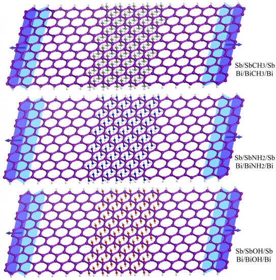
Figure 1.
Bipolar transport device models of Sb/SbXHn/Sb or Bi/BiXHn/Bi double-heterostructure RRTs, where two semi-infinite electrodes are specified at two terminals of Sb or Bi monolayer nanoribbons. Purple, gray, blue, red and white spheres represent the chemically bonding atoms of Sb or Bi, carbon, nitrogen, oxygen and hydrogen respectively. Shallow blue and deep blue colors indicate buffer and electrode regions respectively.
Geometry optimizations of these nanoribbons and their double-heterostructures are performed by Smart iteration algorithm until iteration energy difference, atomic force and atom displacement are less than 0.02 kcal/mol, 0.1 kcal/mol/Å and 0.001 Å, respectively. Quantum ballistic conduction spectra (electron transmission spectra) and current versus voltage variation profiles of Sb/SbXHn/Sb and Bi/BiXHn/Bi nanoribbon double-heterostructures are calculated by non-equilibrium Green’s function combined with first-principles all electron orbital basis method [32,33,34]. The specified schemes and parameter settings of Dmol3 code adopted to calculate band structure and electron transport are listed in Table 1.

Table 1.
Specifications in band structure and electron transport calculations with Dmol3 code.
3. Results and Discussion
3.1. Electronic Band Structure
For Sb and Bi monolayer nanoribbons, the pz-orbital of Sb or Bi atoms is laterally coupled into a huge delocalized conjugate π bond to form one-dimensional electron gas in monolayer plane. The conjugate π bonding electrons near the two edges of Sb or Bi monolayer nanoribbon give rise to a highly conductive channel along nanoribbon extension direction, which appears in band structure by multiple overlapping metallic bands crossing with Fermi level along G-X path of one-dimensional Brillouin zone, as shown in Figure 2. Although the nontrivial topology of Sb or Bi monolayer keeps their topological nanoribbon edge-states being protected for back-scattering forbidden, the Dirac-point of topological edge-states at Brillouin zone boundary X is significantly higher than Fermi level and cannot be incorporated into metallic bands of one-dimensional electron gas near Fermi level. Nevertheless, when nanoribbon width is raised to Nw > 2, the electronic-state density of Sb or Bi pz-orbitals near Fermi level increases enough to cause the band of topological edge-states just below Fermi level elevating to Fermi level. Consequently, a Dirac cone is formed at Fermi level with a smaller effective electron mass than both the conjugate π bonds at Fermi level and the topological edge-states considerably higher than Fermi level, implying that a significant part of electron-states at Fermi level are under topological protection from back scattering, which is actually a nontrivial topology defined by Chern’s number that will be spin-splitting in broken time-reversal symmetry under magnetic field as 2D free electron gas [39]. For an even wider Sb or Bi monolayer nanoribbon, this character is more evident in band structure.
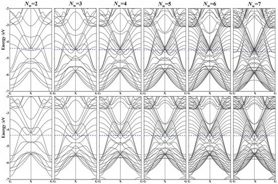
Figure 2.
Band structures of Sb (top panels) and Bi (bottom panels) monolayer zigzag nanoribbons for diverse widths (Nw = 2~7). Vacuum free electron energy is set as energy zero and Fermi level is indicated by horizontal dash line.
As shown in Figure 3 for the calculated band structures of SbXHn or BiXHn monolayer zigzag nanoribbons, the Fermi level, especially for BiCH3 nanoribbon, is overall ~1 eV higher than that of Sb or Bi monolayer zigzag nanoribbons. Surface functionalization on Sb and Bi monolayer nanoribbons causes a complete transformation of band structures near Fermi level, which manifests Z2 invariant (time-reversal symmetry) topological properties derived from hexagonal honeycomb arrangement of Sb or Bi atoms. When Nw > 4, the Z2 invariant topological edge-states on two nanoribbon edges cannot couple each other, and a separate Dirac-cone-like band dispersion is formed at Brillouin zone boundary X point near Fermi level which is slightly higher than Dirac-point. The coupling of topological edge-states between the two nanoribbon edges can open a electronic band-gap and decrease Fermi level, as indicated by the slightly increasing Fermi level with Nw at Nw < 5 and the constant Fermi level at Nw > 4.
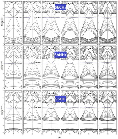
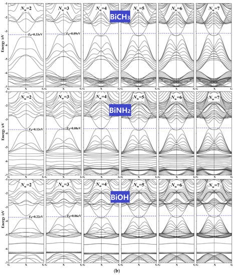
Figure 3.
Band structures of (a) SbXHn and (b) BiXHn monolayer zigzag nanoribbons (Nw = 2~7) with their surfaces being chemically decorated by methyl, amino or hydroxyl group. Vacuum free electron energy is set as energy zero and Fermi level is indicated by horizontal dash line, and Eg denotes energy band gap.
The Fermi level of Sb or Bi monolayer nanoribbon decreases with the increase of Nw, as shown by the left panel in Figure 4. This proves that Fermi-level electron-states are partly derived from the coupled pz-orbitals of the huge delocalized π bond which is subject to the quantum confinement by nanoribbon width, because the energy level of quantum-confined electrons should decrease with confinement dimension. On the contrary, the Fermi level of SbXHn or BiXHn monolayer nanoribbons increases slightly or persists unchanged with the increase of Nw, as shown by the right panel in Figure 4, indicating that Dirac point near Fermi level comes completely from Z2 invariant topological edge-states which is distinguished from electron-states internal nanoribbons.
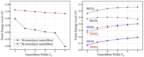
Figure 4.
Fermi energy levels in dependence on nanoribbon width (Nw = 2~7) of Sb or Bi (left panel) and SbXHn or BiXHn (right panel) monolayer zigzag nanoribbons in reference to vacuum free electron energy level.
3.2. Electron Transport in Quantum Resonance
Given that the present nanoribbon double-heterostructure RRTs have mirror or inversion symmetry in atomic structures, it is equivalent of applying positive and negative voltages in opposite directions of bipolar device. Hence, one electrode is arbitrarily chosen as positive electrode and the other one as negative electrode to be applied with Ub/2 and −Ub/2 electrostatic potential, respectively, for the modeled double-heterostructure bipolar devices, where Ub is defined as bias voltage (or voltage bias) and specified in range of 0~1 V to calculate quantum ballistic conduction spectra (electron transmission spectra) and current versus bias voltage (I-Ub) profiles, as shown in Figure 5. A threshold voltage is defined here specifically as the bias voltage where the initial electric current rises to 1/10 of peak current. There is an inevitable Ohmic-like electric conduction due to the coupling between high-mobility topological edge-states of Sb or Bi and SbXHn or BiXHn nanoribbons at Sb/SbXHn or Bi/BiXHn interfaces (heterojunctions), which can be intensified by increasing electric field at these heterojunctions but will approach an uppermost limit at a bias voltage below resonant tunneling threshold.
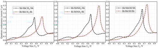
Figure 5.
Quantum conductance I-Ub characteristics of resonant tunneling transistors modeled by Sb/SbXHn/Sb and Bi/BiXHn/Bi double-heterostructures of monolayer zigzag nanoribbons.
When Ub is lower than threshold voltage (Uth = 0.3~0.4 V), the quantum conductance current is still smaller than 1 µA. With the increase of Ub, the Fermi level contributed by topological edge-states of Sb or Bi monolayer nanoribbon segment in the relatively low electric potential area (source region) elevates gradually in these double-heterostructure RRTs, and the triangular energy barrier formed by the quasi Fermi level in central SbXHn or BiXHn nanoribbon segment (tunneling channel) becomes more accurate, which means a decreasing length of tunneling channel. Accordingly, when Ub exceeds Uth, electron resonant tunneling occurs between the topological edge-states of the two constituent Sb or Bi monolayer nanoribbons, and the quantum conductance current increases exponentially with the increase of Ub. Since the transporting electrons near Fermi level are dominantly derived from nanoribbon topological edge-states, for which the back-scattering is forbidden by topological protection, the mobility of electron transport is completely determined by effective electron mass of topological edge-states in these double-heterostructure RRTs. Because the Dirac point of Sb or Bi monolayer nanoribbons becomes more accurate after surface chemical modification by methyl, amino or hydroxyl, that is, the effective electron mass near Fermi level is substantially reduced, the electron mobility of Sb or Bi monolayer nanoribbons is lower than that SbXHn or BiXHn monolayer nanoribbons, which determines the quantum conductance currents of Sb/SbXHn/Sb or Bi/BiXHn/Bi double-heterostructure RRTs. Without gate voltage, the electron resonant tunneling in these nanoribbon double-heterostructures produces the resonant current peak at Ub = 0.55~0.8 V; as bias voltage further increases, the topological conductive channels of the two constituent Sb or Bi nanoribbons in these double-heterostructures begin to stagger, which accounts for the sharply decreasing electron transmission probability and resonant tunneling current with bias voltage, resulting in an extremely high negative differential conductivity.
As shown by the 0.0~1.0 V electron transmission spectra of Sb/SbXHn/Sb and Bi/BiXHn/Bi nanoribbon double-heterostructures in Figure 6, electron resonant tunneling arises when bias voltage is raised to 0.4 V, producing electron transmission peaks in (−Ub/2, +Ub/2) bias window, accounting for the quantum conductance current increasing exponentially with voltage bias. As bias voltage increases to 0.55~0.65 V, the Fermi levels of topological electrons at the two electrodes of Sb/SbXHn/Sb nanoribbon double-heterostructure bipolar devices (RRTs) begin to separate each other when the resonant tunneling turns to ordinary electron tunneling, as manifested by the electron transmission peak near Fermi level shifting out of bias window, which results in a prompt abatement in quantum conductance current and a strong negative differential conductance (NDC) with resonant peak-valley ratios (PVR) of 4.3~4.9. A higher PVR means a longer lifetime of transporting electrons, according to which the optimal working frequency can be effectively set for RRTs. In comparison, Bi/BiXHn/Bi nanoribbon double-heterostructures give rise to strong NDC with PVR of 3.2~4.8 under voltage bias of 0.7~0.8 V.
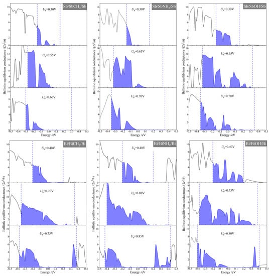
Figure 6.
Electron transmission spectra of resonant tunneling transistors modeled by Sb/SbXHn/Sb and Bi/BiXHn/Bi nanoribbon double-heterostructures.
It has been verified from a recent report that the resonant tunneling current increases sensitively with channel length, whilst persisting on a constant PVR of NDC in BP/silicon-carbide(SiC) nanoribbon double-heterostructure RRT [40]. As illustrated in Figure 2 and Figure 3, in contrast to Sb or Bi monolayer nanoribbons, the SbXHn or BiXHn monolayer nanoribbons exhibit a more accurate Dirac-point of topological edge-states with a lower effective electron mass. Accordingly, it is reasonably suggested for the electron transport characteristics of Sb/SbXHn/Sb and Bi/BiXHn/Bi nanoribbon double-heterostructures as follows: the highly conductive tunneling channel through SbXHn or BiXHn barrier is dominantly derived from nanoribbon topological edge-states, not from quantum confined electrons internal nanoribbons, which are under topological protection from back-scattering in each constituent nanoribbon segment of double-heterostructures; given Nw > 4, the coupling between topological electron-states of the two nanoribbon edges can be avoided, so that resonant tunneling current is independent of nanoribbon width; electron scattering primarily occurs at Sb/SbXHn or Bi/BiXHn heterojunction interfaces, which is determined by energy barrier height and length of central SbXHn or BiXHn monolayer nanoribbon segments.
Therefore, the resonant tunneling current peaks of Sb/SbXHn/Sb and Bi/BiXHn/Bi nanoribbon double-heterostructures decrease exponentially and linearly, respectively, with the increase of NL, while PVR of NDC relies merely on the species of functional group decorated on Sb or Bi nanoribbon surfaces (the higher oxide-ability of functional group used for surface chemical decoration results in a higher electron barrier and PVR), as shown in Figure 7. The recently reported PVR of the nanoribbon RRTs constituted with different monolayer materials are listed in Table 2, indicating that Sb/SbXHn/Sb and Bi/BiXHn/Bi nanoribbon double-heterostructures have higher PVR values than graphene/BN/graphene and GaN/Al/GaN nanoribbon double-heterostructures, which implies they are more efficient nanochannels for RTTs.
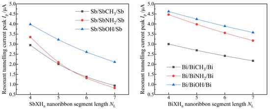
Figure 7.
Quantum conductance current peaks (Ip) of electron resonant tunneling for Sb/SbXHn/Sb (left panel) and Bi/BiXHn/Bi (right panel) nanoribbon double-heterostructures (Nw = 5) in dependence on the length (NL) of central SbXHn or BiXHn nanoribbon segments.
Table 2.
Threshold gate voltage and PVR for resonant tunneling transistors of nanoribbon double-heterostructures constructed by specific 2D monolayer materials.
4. Conclusions
Fermi levels of Sb or Bi monolayer nanoribbons are determined by the infinite delocalized π bond similar to one-dimensional electron gas, while nanoribbon topological edge-states arise at Brillouin zone boundary X point with evidently higher or slightly lower energy levels than Fermi level. Topological edge-states of Sb or Bi monolayer nanoribbon can be merged into Fermi level by increasing nanoribbon width and thus contribute to electron transports with an extremely high mobility under partly topological protection. Surface functionalized Sb and Bi monolayer nanoribbons present a pure Dirac-cone near Fermi level derived from nanoribbon topological edge-states, which accounts for electron transports completely under topological protection without back-scattering. Sb/SbXHn/Sb and Bi/BiXHn/Bi nanoribbon double-heterostructures render a significant resonant current peak with a strong negative differential conductance (NDC) in a narrow voltage bias range by the resonant tunneling of nanoribbon topological edge-states. Resonant current peaks of these simulated double-heterostructure resonant tunneling transistors increase exponentially and linearly with the lengths of central SbXHn and BiXHn tunneling channels, respectively. In particular, the peak-valley ratio of NDC only depends on the species of functional group used for surface chemical decoration on central tunneling channel and is not affected by channel length. Quantum conductance currents of Sb/SbXHn/Sb and Bi/BiXHn/Bi nanoribbon double-heterostructures are generated from the resonant tunneling of high mobility topological edge-states between the two constituent Sb or Bi nanoribbons, which are independent of nanoribbon width and give maximum NDC peak-valley ratios of 4.9 and 4.8 respectively. The present study suggests that surface-functionalized Sb and Bi monolayers are potential in future applications of ultrahigh-frequency and zero-loss topological nanotransistors.
Author Contributions
Data curation, formal analysis, writing—original draft preparation, writing—review and editing, Q.G.; conceptualization, investigation, project administration, G.Z. All authors have read and agreed to the published version of the manuscript.
Funding
This research is funded by the National Natural Science Foundation of China (Grant No. 51973046).
Institutional Review Board Statement
Not applicable.
Informed Consent Statement
Not applicable.
Data Availability Statement
Theoretical methods and results are available from all the authors.
Conflicts of Interest
The authors declare no conflict of interest.
References
- Zeng, H.; Zhi, C.; Zhang, Z.; Wei, X.; Wang, X.; Guo, W.; Bando, Y.; Golberg, D. “White Graphenes”: Boron Nitride Nanoribbons via Boron Nitride Nanotube Unwrapping. Nano Lett. 2010, 10, 5049–5055. [Google Scholar] [CrossRef] [PubMed]
- Ieong, M.; Doris, B.; Kedzierski, J.; Min, Y. Silicon Device Scaling to the Sub-10-nm Regime. Science 2004, 306, 2057–2060. [Google Scholar] [CrossRef] [PubMed]
- Scalise, E.; Iordanidou, K.; Afanas’ev, V.V.; Stesmans, A.; Houssa, M. Silicene on non-metallic substrates: Recent theoretical and experimental advances. Nano Res. 2018, 11, 1169–1182. [Google Scholar] [CrossRef]
- Ho, P.H.; Chang, Y.R.; Chu, Y.C.; Li, M.K.; Tsai, C.A.; Wang, W.H.; Ho, C.H.; Chen, C.W.; Chiu, P.W. High-Mobility InSe Transistors: The Role of Surface Oxides. ACS Nano 2017, 11, 7362–7370. [Google Scholar] [CrossRef] [PubMed]
- Lv, M.H.; Li, C.M.; Sun, W.F. Spin-Orbit Coupling and Spin-Polarized Electronic Structures of Janus Vanadium-Dichalcogenide Monolayers: First-Principles Calculations. Nanomaterials 2022, 12, 382. [Google Scholar] [CrossRef] [PubMed]
- Mishchenko, A.; Tu, J.S.; Cao, Y.; Gorbachev, R.V.; Wallbank, J.R.; Greenaway, M.T.; Morozov, V.E.; Morozov, S.V.; Zhu, M.J.; Wong, S.L.; et al. Twist-controlled resonant tunnelling in graphene/boron nitride/graphene heterostructures. Nat. Nanotechnol. 2014, 9, 808–813. [Google Scholar] [CrossRef] [PubMed]
- Sucharitakul, S.; Goble, N.J.; Kumar, U.R.; Sankar, R.; Bogorad, Z.A.; Chou, F.C.; Chen, Y.T.; Gao, X.P.A. Intrinsic Electron Mobility Exceeding 103 cm2/(V·s) in Multilayer InSe FETs. Nano Lett. 2015, 15, 3815–3819. [Google Scholar] [CrossRef]
- Marin, E.G.; Marian, D.; Iannaccone, G.; Fiori, G. First-Principles Simulations of FETs Based on Two-Dimensional InSe. IEEE Electron. Device Lett. 2018, 39, 626–629. [Google Scholar] [CrossRef]
- Pi, S.; Lin, P.; Xia, Q. Fabrication of sub-10 nm metal nanowire arrays with sub-1nm critical dimension control. Nanotechnology 2016, 27, 464004–464009. [Google Scholar] [CrossRef]
- Lawrence, T.C.; Vashishtha, V.; Shifren, L.; Gujja, A.; Sinha, S.; Cline, B.; Ramamurthy, C.; Yeric, G. ASAP7: A 7-nm film FET predictive process design kit. Microelect. J. 2016, 53, 105–115. [Google Scholar]
- Guo, Y.G.; Wang, F.Q.; Wang, Q. An all-carbon vdW heterojunction composed of penta-graphene and graphene: Tuning the Schottky barrier by electrostatic gating or nitrogen doping. Appl. Phys. Lett. 2017, 111, 073503. [Google Scholar] [CrossRef]
- Punniyakoti, S.; Sivakumarasamy, R.; Vaurette, F.; Joseph, P.; Nishiguchi, K.; Fujiwara, A.; Clement, N. Hydrogen Silsesquioxane-Based Nanofluidics. Adv. Mater. Interface. 2017, 4, 1601155. [Google Scholar] [CrossRef]
- Teong, H.; Lam, K.T.; Khalid, S.B.; Liang, G. Shape effects in graphene nanoribbon resonant tunneling diodes: A computational study. J. App. Phys. 2009, 105, 084317–084321. [Google Scholar] [CrossRef]
- Britnell, L.; Gorbachev, R.V.; Geim, A.K.; Ponomarenko, L.A.; Mishchenko, A.; Greenaway, M.T.; Fromhold, T.M.; Novoselov, K.S.; Eaves, L. Resonant tunnelling and negative differential conductance in graphene transistors. Nat. Commun. 2013, 4, 1794. [Google Scholar] [CrossRef] [PubMed]
- Ongun Özçelik, V.; Durgun, E.; Ciraci, S. Modulation of electronic properties in laterally and commensurately repeating graphene and boron nitride composite nanostructures. J. Phys. Chem. C 2015, 119, 13248–13256. [Google Scholar] [CrossRef]
- Zhang, S.T.; Sun, Z.; Zhao, L. First-principles study of graphene nanoflakes with large spin property. Act. Phys. Sin. 2018, 67, 187102. [Google Scholar] [CrossRef]
- Zhang, P.F.; Liu, Z.; Duan, W.; Liu, F.; Wu, J. Topological and electronic transitions in a Sb(111) nanofilm: The interplay between quantum confinement and surface effect. Phys. Rev. B 2013, 85, 201410. [Google Scholar] [CrossRef]
- Huang, Z.Q.; Chuang, F.C.; Hsu, C.H.; Liu, Y.T.; Chang, H.R.; Lin, H.; Bansil, A. Nontrivial topological electronic structures in a single Bi(111) bilayer on different substrates: A first-principles study. Phys. Rev. B 2013, 88, 165301. [Google Scholar] [CrossRef]
- Wada, M.; Murakami, S.; Freimuth, F.; Bihlmayer, G. Localized edge states in two-dimensional topological insulators: Ultrathin Bi films. Phys. Rev. B 2011, 83, 121310. [Google Scholar] [CrossRef]
- Yang, Z.Q.; Jia, J.F.; Qian, D. Two-dimensional topological insulators with large bulk energy gap. Chin. Phys. B 2016, 25, 117312. [Google Scholar] [CrossRef]
- Wang, Z.F.; Yao, M.Y.; Ming, W.; Miao, L.; Zhu, F.; Liu, C.; Gao, C.L.; Qian, D.; Jia, J.F.; Liu, F. Creation of helical Dirac fermions by interfacing two gapped systems of ordinary fermions. Nat. Commun. 2013, 4, 1384. [Google Scholar] [CrossRef] [PubMed]
- Wu, J.; Xie, L.M.; Li, Y.; Wang, H.; Ouyang, Y.; Guo, J.; Dai, H.G. Controlled chlorine plasma reaction for noninvasive graphene doping. J. Am. Chem. Soc. 2011, 133, 19668–19671. [Google Scholar] [CrossRef] [PubMed]
- Jiang, S.; Krymowsk, K.; Asel, T.; Arguilla, M.Q.; Cultrara, N.D.; Yanchenko, E.; Yang, X.; Brillson, L.J.; Windl, W.; Goldberger, J.E. Tailoring the Electronic Structure of Covalently Functionalized Germanane via the Interplay of Ligand Strain and Electronegativity. Chem. Mater. 2016, 28, 8071–8077. [Google Scholar] [CrossRef]
- Wu, Z.S.; Ren, W.; Gao, L.; Zhao, J.; Chen, Z.; Liu, B.; Tang, D.; Yu, B.; Jiang, C.; Cheng, H.M. Synthesis of Graphene Sheets with High Electrical Conductivity and Good Thermal Stability by Hydrogen Arc Discharge Exfoliation. ACS Nano 2009, 3, 411–417. [Google Scholar] [CrossRef] [PubMed]
- Bagri, A.; Grantab, R.; Medhekar, N.V.; Sheno, V.B. Stability and Formation Mechanisms of Carbonyl- and Hydroxyl-Decorated Holes in Graphene Oxide. J. Phys. Chem. C 2010, 114, 12053–12061. [Google Scholar] [CrossRef]
- Ma, Y.D.; Dai, Y.; Kou, L.Z.; Frauenheim, T.; Heine, T. Robust two-dimensional topological insulators in methylfunctionalized bismuth, antimony, and lead bilayer films. Nano Lett. 2015, 15, 1083–1089. [Google Scholar] [CrossRef]
- Jiang, S.S.; Butler, S.; Bianco, E.; Restrepo, O.D.; Windl, W.; Goldberger, J.E. Improving the stability and optical properties of germanane via one-step covalent methyl-termination. Nat. Commun. 2014, 5, 3389. [Google Scholar] [CrossRef]
- Qiu, J.; Fu, H.; Xu, Y.; Zhou, Q.; Meng, S.; Li, H.; Chen, L.; Wu, K. From Silicene to Half-Silicane by Hydrogenation. ACS Nano 2015, 9, 11192–11199. [Google Scholar] [CrossRef]
- Özçelik, V.O.; Cahangirov, S.; Ciraci, S. Stable Single-Layer Honeycomblike Structure of Silica. Phys. Rev. Lett. 2014, 112, 246803. [Google Scholar] [CrossRef]
- Knapp, D.; Brunschwig, B.S.; Lewis, N.S. Chemical, Electronic, and Electrical Properties of Alkylated Ge(111) Surfaces. J. Phys. Chem. C 2010, 114, 12300–12307. [Google Scholar] [CrossRef]
- Gong, Q.; Zhang, G. Spin-Orbit Coupling Electronic Structures of Organic-Group Functionalized Sb and Bi Topological Monolayers. Nanomaterials 2022, 12, 2041. [Google Scholar] [CrossRef] [PubMed]
- Madsen, G.K.H.; Singh, D.J. BoltzTraP. A code for calculating band-structure dependent quantities. Comput. Phys. Commun. 2006, 175, 67–71. [Google Scholar] [CrossRef]
- Gunst, T.; Markussen, T.; Stokbro, K.; Brandbyge, M. First-principles method for electron-phonon coupling and electron mobility: Applications to two-dimensional materials. Phys. Rev. B 2016, 93, 035414. [Google Scholar] [CrossRef]
- Pecchia, A.; Penazzi, G.; Salvucci, L.; Di Carlo, A. Non-equilibrium Green’s functions in density functional tight binding: Method and applications. New J. Phys. 2008, 10, 065022. [Google Scholar] [CrossRef]
- Perdew, J.P.; Ruzsinszky, A.; Csonka, G.I.; Vydrov, O.A.; Scuseria, G.E.; Constantin, L.A.; Zhou, X.; Burke, K. Restoring the Density-Gradient Expansion for Exchange in Solids and Surfaces. Phys. Rev. Lett. 2008, 100, 136406. [Google Scholar] [CrossRef]
- Kadek, M.; Repisky, M.; Ruud, K. All-electron fully relativistic Kohn-Sham theory for solids based on the Dirac-Coulomb Hamiltonian and Gaussian-type functions. Phys. Rev. B 2019, 99, 205103. [Google Scholar] [CrossRef]
- Monkhorst, H.J.; Pack, J.D. Special points for Brillouin-zone integrations. Phys. Rev. B 1976, 13, 5188. [Google Scholar] [CrossRef]
- Ghanbari Shohany, B.; Roknabadi, M.R.; Kompany, A. Electrical investigation of armchair graphene-graphdiyne-graphene nanoribbons heterojunctions. Commun. Theor. Phys. 2016, 65, 99–104. [Google Scholar] [CrossRef]
- Chang, C.Z.; Zhang, J.S.; Feng, X.; Shen, J.; Zhang, Z.C.; Guo, M.H.; Li, K.; Ou, Y.B.; Wei, P.; Wang, L.L.; et al. Experimental Observation of the Quantum Anomalous Hall Effect in a Magnetic Topological Insulator. Science 2013, 340, 167–170. [Google Scholar] [CrossRef]
- Dong, J.; Li, H.; Li, L. Multi-functional nano-electronics constructed unsing boron phosphide and silicon carbide nanoribbons. NPG Asia Mater. 2013, 5, e56. [Google Scholar] [CrossRef]


Disclaimer/Publisher’s Note: The statements, opinions and data contained in all publications are solely those of the individual author(s) and contributor(s) and not of MDPI and/or the editor(s). MDPI and/or the editor(s) disclaim responsibility for any injury to people or property resulting from any ideas, methods, instructions or products referred to in the content. |
© 2023 by the authors. Licensee MDPI, Basel, Switzerland. This article is an open access article distributed under the terms and conditions of the Creative Commons Attribution (CC BY) license (https://creativecommons.org/licenses/by/4.0/).