Abstract
The bottleneck for large-scale processing within perovskite solar cells (PSCs) development is the stringent need for uniform thin films. On a lab scale, the spin coating methodology with acceptable uncertainty ensures a high level of uniformity with minimal roughness, no voids, and reproducible procedures. However, the technique is strongly limited for up-scaling because the uncertainty is out of range from the spin center to the edge, resulting in areas only up to a few cm2. In order to boost the industrialization of PSCs, the spray coating (SC) methodology can represent a good solution for achieving the goal of uniformity (in terms of crystal size, film thickness, and roughness) that, combined to a reduced active materials waste, compatible to roll2roll production line, will pave the way to PSCs mass production. In this critical review, we present the technological features of SC relevant to PSCs development and critically discuss the key points on which to address the focus for achieving optimal and reliable performances in connection with the fundamental higher potential of SC over spin-coating in allowing to control thin film homogeneity. This review can help in the commercialization of perovskite solar cells but also can contribute to the development of scale-up methodologies.
1. Introduction
The possibility of processing perovskite thin film through wet-chemistry approaches makes the fortune of this emerging technology in the world of third-generation photovoltaics (PV). After a decade of research, the power conversion efficiency (PCE) of perovskite solar cells (PSC) has risen from 3.8% to 25.7% [1]. However, mass adoption is strongly affected by the lack of industrially compatible coating techniques that guarantee large-scale module manufacturing. In fact, a loss in efficiency is found when the module area is increased: the reason may be ascribable to higher series resistance, lower shunt resistance, and mainly non-uniform coatings [2]. Figure 1A demonstrates how classical PV technologies follow an inverse up-scaling law with the increasing area while PSCs do not, probably because limited efforts were dedicated to modifying the uniform property.
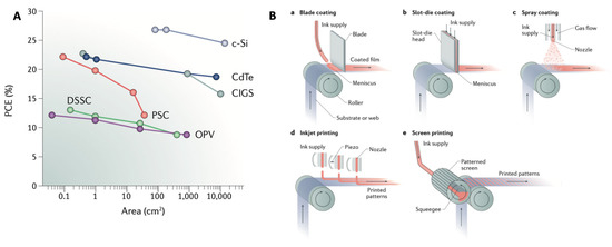
Figure 1.
(A) Effect of active layer size on PV PCE for different technologies. (B) Roll-to-roll techniques for PSC development. (c-Si, crystalline silicon; CdTe, cadmium telluride; CIGS, copper indium gallium selenide; DSSC, dye-sensitized solar cell; OPV, organic PV). Adapted with permission from Springer Nature: Ref. [2], © 2023.
Currently, the lab-scale production of multi-layer PSC devices is mainly performed via spin coating, a technique useful for achieving fast, reproducible, and uniform thin films, although only on a reduced scale (in the order of 1 cm2). Another strong limitation of spin coating is the high volume of precursor consumption since less than 1% of what is disposed of actually ends up on the substrate during processing. Although the perovskite precursors are relatively cheap, the ancillary layers constituting the cells as a whole are more expensive: for example, SPIRO-OMeTAD—the current benchmark for hole transporting layers in PSCs—costs about 500 USD/g, and its stability is compromised by the presence of hygroscopic additives [3].
Therefore, the scientific community has attempted to apply different processing methodologies for efficient PSC scale-up, such as blade-coating, slot-die coating, inkjet printing, screen printing, and spray coating (SC) (see Figure 1B). All of these techniques are suitable for industrial up-scaling. However, several limitations may occur from each one of them. For instance, the quality of films prepared by blade-coating is affected by the high speed of the roll, with the formation of scratches or spits, and, generally, films with thicknesses below 10 μm are difficult to control. Slot-die coating, the ideal technique for scaling up in solution processable PV, is based on a very complex system that requires a deep understanding of the physics behind it since many parameters affect the final quality of the films, such as flow rate, speed, upstream pressure difference, attack angle, and head design. Printing techniques widely used for metal contact development in standard silicon PV are not suitable for non-flat substrates, limiting, for example, the development of efficient textured silicon-perovskite tandem solar cells, an emerging alternative to single-junction PSCs [4]. SC deposition, with its best-performing version equipped with ultrasonic spraying (US) system, allows obtaining uniform thin films, reduced waste, and, mostly, the possibility of realizing thin films on rough substrates without voids [5].
The saving of reagents is an important aspect to be considered when using SC technology. For instance, Figure 2 shows how the Pb waste can be substantially reduced when the SC technique is coupled to chemical vapor deposition (CVD) and used in a two-step processing instead of spin coating and how the effect is notably enhanced when the substrate size increases [2].
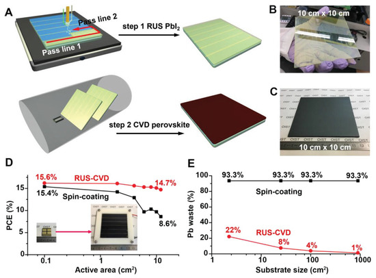
Figure 2.
PCE and lead waste during perovskite deposition processes as a function of substrate size. (A) Schematic drawing of the RUS–CVD perovskite film deposition technology. PbI2films are RUS coated on the FTO/c-TiO2 substrates, and converted to FAPbIxBr3−x via a CVD process. Photographs of (B) a RUS-coated PbI2 film before annealing and (C) a CVD-converted FAPbIxBr3−x film deposited on a 10 cm × 10 cm patterned FTO substrate. (D) Solar cell and module performance as a function of active area. Spin-coating data are extracted from cited literature in ref. [12]. The RUS–CVD method shows much lower substrate size dependence than the spin-coating method. (E) Lead waste during the perovskite deposition process as a function of substrate size. Lead waste during the RUS–CVD process continuously decreases until it becomes negligible, much less than that generated during the spin-coating process. Reprinted from Ref. [12] with permission of Wiley-VCH.
Lead waste is not a unique source of pollution deriving from PSCs. Indeed, some of us have recently reported a case [6] of a carbon-based PSC with a Cs2AgBiBr6 light absorber, developed using ultrasonic SC for the processing of the top carbon electrode: an interesting achievement, particularly for the possibility of resorting to conductive carbon derived from waste-tires. The use of this protocol allowed us to achieve a record 1.293 V open-circuit voltage (Voc) in the final devices. Therefore, sustainable end-of-life and end-of-waste approaches are surely added values for PSC development, and we address the reader to take a deeper look at these topics by reading the relevant recent literature [7,8,9].
The main parameters that can be tuned during the SC processing hugely affect the quality of the resulting thin films. Trivially, the most important one is the size of the droplets that largely impact the final crystal grain size. For this reason, a piezoelectric transducer is used to reduce the average dimension of the droplets with respect to conventional airbrushes [10,11].
Indeed, the US system operates by converting high-frequency sound waves into mechanical energy that is transferred into a liquid, thus creating standing waves. When the liquid goes out from the nozzle, it undergoes atomization by the formation of a haze of uniform micron-sized droplets. The liquid is usually pumped towards the nozzle exit and atomized by US vibrations. Nowadays, there are several versatile instruments available on the market dedicated to R & D purposes (both academic and industrial-oriented), and most of them offer implementation for solar-related purposes, thus underlying how the SC methodology can be beneficial for last-generation PV development. A brief list of companies focusing on spray-based technology includes Sono-Tek, USI, Microspray and Sonoaer in the USA, Siansonic, Cheersonic and CYCO in China, Trident and Analytical Technologies in Singapore, Nadetech in Spain, and Veco in The Netherlands.
The first example in the literature of a PSC made via US SC was a work of the group of Lidzey [13], in which 11% PCE was reported after applying a single-pass deposition of a solution of lead chloride and methylammonium iodide to obtain the CH3NH3PbI3−xClx perovskite. The study highlighted the combined role of the temperature of the substrate during spray-casting, the volatility of the casting solvent, and the choice of the post-deposition annealing temperature as key factors in determining a good perovskite quality. After that, several works came out with the scope of improving the figures of merit of US-spray coated PSCs, trying to replicate what is usually achieved with spin coating: use of two-step depositions [13], multiple passing [14], different bath treatments [14,15], and/or playing with the chamber pressure during deposition [16]. From the same group of the first report, an interesting finding was reported, in which a 19.4% PCE and a 12.7% stabilized PCE were obtained on an active area of about 1 cm2 by connecting several cells in parallel [17]. To the best of our knowledge, the actual record PCE was achieved by Cai et al. with a 20% obtained after proper optimization of parameters, also bringing to long-term stability (devices retained about 85% of the initial efficiency after 650 h storage in a dry environment) [18]. There are also several recent review papers that present the latest results about spray-coated PSCs in terms of efficiency and performance [10,19,20,21].
With this critical mini-review, we want to briefly discuss the most important achievements in the field of SC of PSCs by understanding the role of each contribution in relation to thin films uniformity (crystal size, roughness, and film thickness), with the scope of focusing on final market mass adoption. In this way, we aim to suggest valuable hints, especially the uniformity and growth path of perovskites, for the industrial production and commercialization of PSCs.
2. Achieving Crystal Size Uniformity
Uniformity is an essential quality in perovskite solar cell development. The importance of controlling local chemistry in perovskite-based devices is fundamental for producing high-performing solar cells with ease of reproducibility. In particular, the different preparation methods affect grain boundaries during thin film formation. Generally speaking, we can easily assume that a uniform thin film can be obtained only when the crystal growth mechanism is finely monitored, and this can happen when the surface chemistry is well determined.
As discussed by Lee et al. [22], the crystal growth mechanism for perovskites during spin coating can be described by a La Mer model (Figure 3A): the concentration of the solution increases until it reaches the supersaturation concentration (Cs), where the formation of perovskite nuclei takes place (Stage I). In the following step (Stage II), the growth enters a diffusion-limited regime determined by the solute uptake: the solution concentration goes down below the Cs point when the evaporation of the solvent becomes slower than the consumption of the solute. In this way, the growth is favored with respect to new nuclei formation (Stage III). This approach can be acceptable also for SC (Figure 3B), with the strong difference that while spraying, the diffusion-limited regime is notably quenched because what determines the crystal growth regime is the balance between the evaporation time of the solvent (te) and the time required for covering an area (tc) [23]. Only when te is slightly bigger than tc can a smooth film be obtained. A good strategy is to choose an opportune nozzle-to-sample distance (NSD) that allows the reaching of a dilute/very dilute number of small droplets on the surface [23] (Figure 3C).
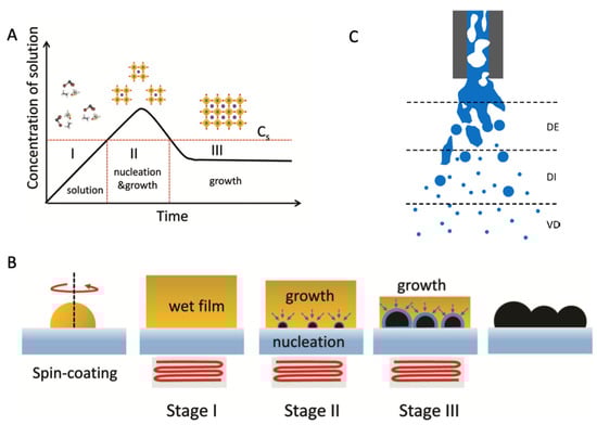
Figure 3.
(A) Lar Mer model for nucleation and growth of perovskite thin films. Cs is the supersaturation concentration of a precursor solution. (B) A schematic illustration of nucleation and growth of perovskite films at each stage. Reprinted from Ref. [22] with permission from Wiley-VCH. (C) Schematic representation of the three flow regimes, based on spraying for fuel combustion, during atomization: dense (DE), dilute (DI), and very dilute (VD) with respect to the concentration of the liquid in the spray cone. © IOP Publishing. Reproduced with permission [23]. All rights reserved.
Several strategies have been implemented to improve the crystal size uniformity of the grains. For example, Park et al. recently decided to increase the frequency of the US for strongly affecting the final dimension of the droplets [24]: they applied a 1.7 MHz generator to create a narrower distribution of droplets dimensions (2–4 microns) that is notably different from the usual 10-micron droplets forming when <1 MHz ultrasonic generators are used. In this work, they showed how the speed rate tuning allows fine-tuning of the crystal size uniformity achieving a 350–900 nm grain size difference in the various ranges. They finally obtained a PCE of 14.2% for a large-area device (1 cm2).
Amalathas and coworkers [25] acted on the depositing substrate. They found that, by treating the underlying titania electrode, larger crystals can be obtained, positively affecting the sub-band-gap deep defects at the interface of the perovskite and suppressing non-radiative recombination. In this way, they reached up to 20% PCE. Furthermore, in a recent article [26], the authors optimized the te and the tc parameters for allowing fast solvent evaporation and, at the same time, fast film formation within a few seconds without post-annealing treatment, thus achieving 13.5% for the MAPbI3 perovskite in air condition with high humidity.
Particular attention may be given to the work of Heo et al. [27], in which a 14% PCE for devices with 112 cm2 active area was achieved with only 9% degradation after a prolonged continuous illumination of 1000 h. In that work, they show the great capability of fabricating uniform areas with SC with respect to the spin coating approach on 6 × 8 cm2 substrates (Figure 4, top panel). In the case of spin coating, there are clearly non-uniform ring features from the center to the outside edge of the film, as noticeable by the SEM images. The authors explain this result with the different kinetics connected to the evaporation of the solvent at the center of the sample and on the borders. On the other hand, SC allows uniform crystallization and film formation over the entire substrate without any differences. The resulting figures of merit of the device are consistent with the morphology comparison of spray- and spin-coated perovskite thin films (Figure 4, bottom panel).
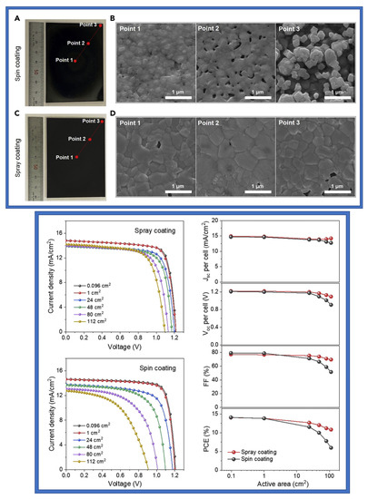
Figure 4.
Large area coating of perovskite films by spin and spray coatings (SEM analysis, top panel) and corresponding device analysis (bottom panel). Top panel: Large-Area Coating of CsPbI2Br Perovskite Films. (A,B) Photograph (A) and SEM images (B) of CsPbI2Br thin film by spin coating. (C,D) Photograph (C) and SEM images (D) of CsPbI2Br thin film by spray coating. The substrate area is about 6 cm × 8 cm. Bottom panel: PV Characteristics of Spray-Coated and Spin-Coated CsPbI2Br Perovskite Solar Cells and Submodules J-V curves of spray-coated and spin-coated devices with device aperture area varying from 0.096 to 112 cm2. J-V curves are plotted on a per-cell basis. Comparison of the PV parameters for spray- and spin-coated devices as a function of device area. Reprinted from [27], Copyright 2021, with permission from Elsevier.
3. Achieving Uniform Thickness and Roughness
High-quality perovskite films show uniform surface roughness and controlled thickness. The main reason derives from the need for smooth surfaces for reducing recombination centers for photocharges, thus limiting the figures of merits of a cell (mainly Voc). Casting techniques usually undergo film shrinkage and/or volume expansion of the lead iodide precursor during solvent annealing. Altogether these aspects may cause cracks or pinholes that deteriorate the resulting devices.
By looking at the literature, we can attest that two-step processing is preferable for producing uniform thin films in terms of crystallinity, reduced (or at least controllable) roughness, and tunable thickness. The reasons mainly derive from the poor film coverage in the one-step process due to the fast reaction between PbI2 and CH3NH3I reactants. Therefore, the authors opted first to cover the substrate with lead iodide thin films and then spray the metalorganic salt [28,29,30,31,32]. The big issue with this choice is that to assure a complete, uniform, void-free lead iodide surface, people opted for spin coating for the first pass, thus completely ignoring the scalability, which is the real driving force for exploiting SC. A well-presented and exhaustive review paper has been recently published, focusing on the different features arising from the two diverse approaches [21]. In this section, we focus on the relevant literature that gives a rational perspective on how it could be possible to control the roughness and the thickness of spray-coated perovskite layers.
The thickness of the perovskite layer is directly linked to the efficiency of the device: the higher the thickness, the higher the current will be since more incident light can be absorbed. However, if the perovskite is too thick, the charge extraction is more difficult, causing a reduced current. Therefore, the optimal thickness is in the range of 300–600 nm. When using the spin coating methodology, the resulting thin films are very flat (average roughness, Ra, below 5 nm). On the contrary, when using SC, the roughness (notably higher than when using spin coating) can be finely tuned by simply changing the flow rate of the nozzle and/or the spray speed rate without affecting the overall performance [15].
The wetting governs the resulting hydrophilicity of the film. In fact, droplets deposited on a hydrophilic surface will spread, covering a large area. This effect can influence the moisture capabilities of the device, which need to be more hydrophobic to avoid water uptake (that causes perovskite decomposition). In a recent paper [33], the differences in the contact angle of water drops for spray and spin-coated perovskite films are compared: the spray coated showed more hydrophobic behavior (74°) than the spin-coated one (63°), thus confirming the long-term stability data, in which the former devices show the capability of maintaining the initial performances for more than 80% (only 57% for the spin-coated). This result agrees with the improved roughness of the spray-coated surface.
Generally, the roughness increases with the number of passes and the thickness of the film. Hence, shorter deposition times and pulsed operation would be preferable. In addition, a high temperature of the substrates increases the roughness because the evaporation time reduces. At the same time, coffee rings effects diminish. A rational way to affect the roughness of the film is to apply a bias during the deposition: in this way, with the electric field, the atomization is improved, and the roughness passes from 39 nm to 19 nm [34].
Another interesting way to reduce the roughness is to exploit the vacuum-assisted technology [35]: the authors applied a one-step deposition process in which they sprayed the triple cations-precursor ink all at once on an ITO/SnO2 substrate held at 40°, then put the device in low-vacuum for some minutes for allowing the DMF extraction from the wet film, and finally annealed at 100°. The treatment is beneficial for the roughness: it passes from a value of 100 nm to a value of 22 nm, with a maximum PCE value of about 18%.
The rational understanding of the physics behind spray processes allows us to make simulations and thus develop predictive models for reducing roughness and optimizing spraying parameters. This is what some authors performed in a study in which they developed a discrete element method-based multiscale model to accurately describe the interplay between the macroscopic phenomenon (i.e., heat and mass transfer) and the microscopic molecular interactions, with the final aim of predicting the optimal parameters (spray angle and deposition rate) for perovskite quantum dot-based thin film processing [36]. In this regard, it is worth highlighting that SC is likely the best technique to use when intending to fabricate optoelectronic devices such as solar cells or light-emitting diodes from nanomaterials-based inks (quantum dots, perovskite nanocrystals, etc.).
The resulting roughness, indeed, is strongly affected by the amount of volume (V) of the as-deposited wet film as evidenced by the recent work [35]: V is linearly proportional to the spray flow rates and inversely to the stage speed and the distance between nozzle and substrate. The authors show that if a too-wet or too-dry film is obtained, the roughness (but not the thickness) is hugely increased (Figure 5). Therefore, a threshold volume value (V0) needs to be found to obtain very smooth and uniform thin films after soaking and annealing. In addition, this precise tuning of the ink volume allows for widening the processing window of the following soaking step to 45 min, boosting the reproducibility of the whole process from an industrialization point of view.
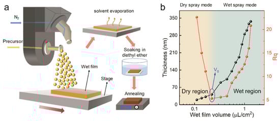
Figure 5.
Sprayed film deposition mode. (a) Schematic illustration of a single-pass spray-coated perovskite film produced in wet spray mode. (b) Thickness and roughness of perovskite films as a function of the volume of the sprayed precursor on the substrate. V0 was the threshold of the dry region, which represents dry spray mode, and the wet region, which represents wet spray mode. The sprayed process at the dry region is defined as the dry region mode, and the sprayed process at the wet region is defined as the wet spray mode. Reprinted with permission from [35]. Copyright 2020 American Chemical Society.
4. Characterization of Large-Area Thin Film
The previous paragraphs highlight the technical difficulties in the preparation of homogeneous perovskite films and devices in the development process from laboratory-scale, small-area films to industrial-scale, large-area ones. Characterization methods for large-area thin films are also very relevant for both the scientific research community and the industry, and they are of great value for revealing crystal structure, defect sites, thin film uniformity, properties of interfaces and contacting layers, module performance, failure mechanism, etc. Characterization results can also effectively guide the obtainment of uniform thin films through SC. Thus, we here describe the relevant characterization methods and effects of their use from four different points of view: material structure, film uniformity, defect properties, and device performance.
The basic properties of materials, such as composition, crystal structure, absorption bandgap, and morphology, are the first prerequisites for understanding the growth process of perovskite thin films. The characterization techniques widely used in small-area films are mainly optical microscopy, scanning electron microscopy (SEM), confocal laser scanning microscopy (CLSM), atomic force microscopy (AFM), X-ray diffraction (XRD), UV–vis spectrophotometry, photoluminescence (PL), X-ray photoelectron spectroscopy (XPS), and UV photoelectron spectroscopy (UPS). When they constitute multi-site tests, they can also reflect the quality of large-area films [5,15,27,30,37].
For example, XRD, UV–vis measurements, and AFM were performed on six different locations of each 5 cm × 5 cm substrate to study the chemical composition, crystal structure, absorbance edges, and morphology of the perovskite films (Figure 6A–I) [12]. XRD patterns on the same sample but at different positions are similar, suggesting these data represent a large area (Figure 6B). The variation of absorbance at a wavelength between 600 and 700 nm on the same sample but at different sites is six to eight times smaller for films prepared through the raster US SC (i.e., in which the spraying head can move in both the x and y axes) combined to chemical vapor deposition (RUS–CVD) method compared to films prepared via raster US SC combined with dipping coating (RUS-D), suggesting the perovskite film prepared by RUS–CVD is more uniform at the macroscopic scale (detection area is 0.3 cm × 0.5 cm for each measurement) (Figure 6C, inset). Absorbance edges for the two perovskite films are both at ≈790 nm. In addition, all the AFM images consistently show that the films converted from the compact PbI2 (DMF:DMSO = 14:0.65 for RUS) have a high degree of uniformity [12].
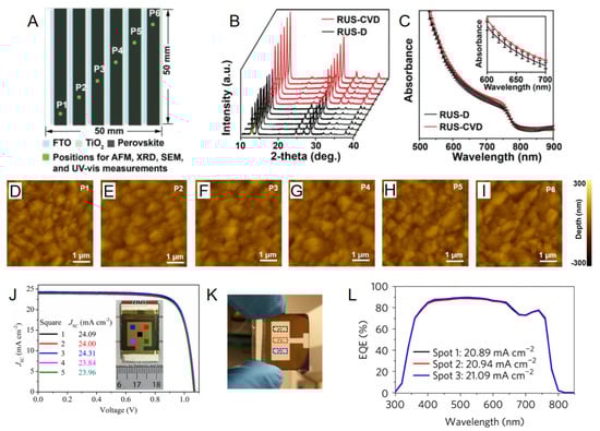
Figure 6.
(A) Schematic drawing showing the six positions for the XRD, UV–vis measurements, and AFM carried out on perovskite films prepared through RUS-D and RUS-CVD methods. (B) XRD pattern of the six intentionally selected points. (C) UV–vis absorbance spectra of the six intentionally selected points. (D–I) AFM images of the six intentionally selected points. Reprinted from Ref. [12] with permission from Wiley-VCH. (J) Photovoltaic parameters from five different spots with an aperture area of 0.16 cm2 were selected from the total active area of 1.2 × 1.2 cm2 under standard AM 1.5 G illumination. Reprinted from Ref. [38] Copyright 2016, Science. (K,L) EQE spectra from three different spots on a large-area (>1-cm2) cell. Reprinted from Ref. [39]. Copyright 2017, Springer Nature.
Some advanced mapping technologies are currently more intuitive, comprehensive, and effective characterization methods to evaluate the homogeneity, defect sites, connection effects, and failure mechanisms of large-area films after preparation. These characterization methods and the technical applications of X-ray fluorescence (XRF) spectroscopy, photoluminescence (PL) mapping, time-resolved photoluminescence (TRPL) mapping, light-beam-induced current (LBIC) mapping, electroluminescence (EL), lock-in thermography (LIT), and scattered light intensity (SLI) imaging are discussed below [12,16,39,40,41,42,43]. The testing principles and differences of these characterization techniques are presented in comparative Table 1.

Table 1.
Some advanced mapping technologies to characterize the uniformity of large-area films.
XRF is the emission of characteristic “secondary” (or fluorescent) X-rays from a material that has been excited by bombarding it with high-energy X-rays or gamma rays. Yang et al. showed the XRF mapping of lead (Pb) in units of mass per area, which attested to the high quality of the blade-coated perovskite films on substrates with an area of several square inches (Figure 7A) [39]. SLI relies on the laser speckle effect. When the laser is irradiated on an optically rough surface or when the laser passes through a scatterer or a space with suspended particles, due to the coherent superposition of light waves, the reflected light field thus formed has a random spatial light intensity distribution, which is indeed called the laser speckle effect. EL is the basic working mechanism of semiconductor light-emitting diodes, and an EL image can provide information about charge recombination at the nanoscale and macroscopic charge-transport obstacles associated with non-uniformity, impurities, shunting, and internal resistance. PL mapping is a spatially resolved technique that can characterize the uniformity and quality of the photoactive layer [2,12,42]. Jiang et al. studied the quality and uniformity of films and devices over the entire module area, performing spatially resolved measurements such as SLI imaging, PL mapping, and EL imaging, which allowed rapid characterization of the entire 5 cm × 5 cm mini-modules and were also compatible with in-line characterization in a production environment (Figure 7B–G) [12]. LBIC mapping uses a small laser spot to scan the active area of solar cells and provides a local photocurrent generation profile of the device. The inhomogeneous current distribution clearly revealed the non-uniformity of the perovskite films. Bishop et al. explored the homogeneity of the spray-cast device photocurrent across the active area through the LBIC mapping technology, and they also performed TRPL mapping of films to understand the uniform of charge carrier lifetimes (Figure 7H,I) [16]. Electrical defects within the absorber appear in a thermography image as hot spots with sharp contours, whereas in an EL image, they appear as dark spots. Thermography can also be used to investigate the losses in interconnection lines between cells, for which EL is unsuitable. In contrast, an EL image reveals the local internal junction voltage distribution, which is especially interesting in the vicinity of a defect. Gerber et al. demonstrated that they could obtain properties of solar modules such as the spatial voltage distribution, the resistances of the front and back contact, and the shunt resistance of local defects through the EL and DLIT images (Figure 7J,K) [41].
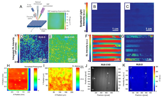
Figure 7.
(A) X-ray fluorescence mapping of lead (Pb) on a typical perovskite film. (B,C) False-color monochrome scattered light optical images of perovskite films. (D,E) False-color monochrome PL mapping images of the FAPb(I0.85Br0.15)3 films. (F,G) False-color monochrome EL mapping images of perovskite modules prepared by (F) RUS–CVD and (G) RUS–D methods. Reprinted from Ref. [12] with permission from Wiley-VCH. (H) LBIC image of the device that includes a perovskite layer. (I) TRPL maps of the spray-casted film. Reprinted with permission from Ref. [15] under CC-BY license. Copyright 2018 American Chemical Society. (J,K) Comparison of an EL image J and a LIT image (K) of a 30 × 30 cm2 CIGS module at an injection current of 0.83 mA cm2. The EL image was captured within 3 s, whereas the measurement duration for the LIT image was 30 min. The letters A, B, and C indicate defects of different strengths. Reprinted from Ref. [41], Copyright 2014, with permission from Elsevier.
In addition, J-V curves and external quantum efficiency (EQE) are essential for testing the performance of large-area devices or modules, while steady-state PL spectra, TRPL, space-charge-limited current (SCLC) measurements, electrochemical impedance spectroscopy (EIS), and J-V characteristics as a function of light intensity (I) are methods for relatively quantitative research on device defects [13,14,24,28,31,35,39,44,45].
Li et al. measured J-V curves at five different small spots (each 0.4 cm by 0.4 cm) located at the centre and the four corners of the device’s active area (Figure 6J). All the PV metrics, including JSC, extracted from these five curves by a black mask with a square aperture area of 0.16 cm2 were almost identical, and the value of JSC shows very small variation when the square aperture area of the mask is increased up to 1 cm2, attesting to the uniformity of the perovskite film over the cm2 scale [38]. Yang et al. reported the EQE spectra from three different spots from the 1.2-cm2 device were indistinguishable, which further attested to the uniformity at the device level using blade coating to produce the perovskite layer (Figure 6K,L) [39]. Huang et al. compared the PL intensity of the sprayed film was almost ten times as high as that of the spin-coated film, and the PL peak showed a little blue shift. These two features implied that the surface defect concentration and non-radiative recombination in the sprayed film were much lower than in the spin-coated one [13]. Duan et al. fitted the corresponding decay times of the TRPL spectra according to a biexponential decay model. The shorter lifetime (t1) and longer lifetime (t2) were mainly assigned to trap-mediated nonradiative recombination and radiative recombination, respectively [31]. Heo et al. calculated the trap densities (Nt) of the spray-coated samples via the SCLC measurement [14]. Su et al. used the EIS to characterize carrier behavior in PSCs. The two semicircles in the Nyquist plots represented the charge transfer resistance (Rct) and the charge recombination resistance (Rrec), respectively. They also showed the liner relationship between voltage (Voc) and light intensity, while the deviation between kT/q and liner slope testifies to trap-assisted recombination [35].
5. Conclusions
The manufacturing of PSCs is entering the most complex but intriguing season of existence. Today, there is indeed a strong need for valuable strategies to allow their large-area fabrication. The procedures for this type of pre-industrial or industrial fabrication scale must obey the modern laws of the current market and society by taking into account reagent saving, reproducibility, long-term stability, and sustainability. In order to meet these requirements, (1) we suggest SC as a valuable technology to resort to, relying on its multiple options (i.e., ultrasonic, raster, megasonic, etc.), which can achieve homogeneous films on a large scale. Compared to the spin-coating technique, SC has more tools for forming a perovskite layer rather than a solo rotating. (2) This upgradeable processing technology, together with different roll-to-roll techniques, can be easily adapted by productions. (3) In addition, we advocate the integration of SLI, EL, LBIC, and LIT, the main mapping technologies for detecting the uniformity of large-area films, into the industrial manufacturing process to real-time detect the prepared film defect sites, hidden cracks, and desoldering. We believe the tendency of real-time detect integrated SC will change the production of perovskite solar cells and modules.
The issues that the scientific community must first solve are the ones related to conventional large-area manufacturing: the search for the obtainment of smooth surfaces, the possibility of controlling the roughness and the wettability of the spray-coated films, and of finely tuning their thickness. Typical morphological and functional characterization techniques can be applied to achieve these goals, with the help of chemists, material scientists, physicists, and engineers, in a multidisciplinary effort that will allow the entrance of PSC into the global PV market.
Funding
This research was funded by H2020 FET-PROACTIVE-EIC-07-2020 grant number [101017821]; and by the Deutsche Forschungsgemeinschaft (DFG, German Research Foundation) grant number GA 3052/1-1; and by the National Natural Science Foundation of China grant number [52202241]; and by the Leading Innovative and Entrepreneur Team of Zhejiang grant number [2019R01012]; and by the new energy innovation program of Huzhou, Zhejiang, China grant number [2021GG36,2022C03042].
Acknowledgments
T.G. would like to acknowledge the Justus Liebig University Giessen for the Herbert-Stolzenberg prize for research 2022.
Conflicts of Interest
The authors declare no conflict of interest.
References
- Best Research-Cell Efficiency Chart. Available online: https://www.nrel.gov/pv/cell-efficiency.html (accessed on 20 January 2023).
- Li, Z.; Klein, T.R.; Kim, D.H.; Yang, M.; Berry, J.J.; van Hest, M.F.A.M.; Zhu, K. Scalable fabrication of perovskite solar cells. Nat. Rev. Mater. 2018, 3, 18017. [Google Scholar] [CrossRef]
- Lamberti, F.; Gatti, T.; Cescon, E.; Sorrentino, R.; Rizzo, A.; Menna, E.; Meneghesso, G.; Meneghetti, M.; Petrozza, A.; Franco, L. Evidence of Spiro-OMeTAD De-doping by tert-Butylpyridine Additive in Hole-Transporting Layers for Perovskite Solar Cells. Chem 2019, 5, 1806–1817. [Google Scholar] [CrossRef]
- Lee, S.-W.; Bae, S.; Hwang, J.-K.; Lee, W.; Lee, S.; Hyun, J.Y.; Cho, K.; Kim, S.; Heinz, F.D.; Bin Choi, S.; et al. Perovskites fabricated on textured silicon surfaces for tandem solar cells. Commun. Chem. 2020, 3, 37. [Google Scholar] [CrossRef] [PubMed]
- Sansoni, S.; De Bastiani, M.; Aydin, E.; Ugur, E.; Isikgor, F.H.; Al-Zahrani, A.; Lamberti, F.; Laquai, F.; Meneghetti, M.; De Wolf, S. Eco-Friendly Spray Deposition of Perovskite Films on Macroscale Textured Surfaces. Adv. Mater. Technol. 2019, 5, 1901009. [Google Scholar] [CrossRef]
- Schmitz, F.; Lago, N.; Fagiolari, L.; Burkhart, J.; Cester, A.; Polo, A.; Prato, M.; Meneghesso, G.; Gross, S.; Bella, F.; et al. High Open-Circuit Voltage Cs 2 AgBiBr 6 Carbon-Based Perovskite Solar Cells via Green Processing of Ultrasonic Spray-Coated Carbon Electrodes from Waste Tire Sources. ChemSusChem 2022, 15. [Google Scholar] [CrossRef]
- Goetz, K.P.; Taylor, A.D.; Hofstetter, Y.J.; Vaynzof, Y. Sustainability in Perovskite Solar Cells. ACS Appl. Mater. Interfaces 2020, 13, 1–17. [Google Scholar] [CrossRef]
- Kadro, J.M.; Hagfeldt, A. The End-of-Life of Perovskite PV. Joule 2017, 1, 29–46. [Google Scholar] [CrossRef]
- Dou, J.; Bai, Y.; Chen, Q. Challenges of lead leakage in perovskite solar cells. Mater. Chem. Front. 2022, 6, 2779–2789. [Google Scholar] [CrossRef]
- Bishop, J.E.; Routledge, T.J.; Lidzey, D.G. Advances in Spray-Cast Perovskite Solar Cells. J. Phys. Chem. Lett. 2018, 9, 1977–1984. [Google Scholar] [CrossRef]
- Bishop, J.E.; Smith, J.A.; Lidzey, D.G. Development of Spray-Coated Perovskite Solar Cells. ACS Appl. Mater. Interfaces 2020, 12, 48237–48245. [Google Scholar] [CrossRef]
- Jiang, Y.; Remeika, M.; Hu, Z.; Juarez-Perez, E.J.; Qiu, L.; Liu, Z.; Kim, T.; Ono, L.K.; Son, D.; Hawash, Z.; et al. Negligible-Pb-Waste and Upscalable Perovskite Deposition Technology for High-Operational-Stability Perovskite Solar Modules. Adv. Energy Mater. 2019, 9, 1803047. [Google Scholar] [CrossRef]
- Huang, H.; Shi, J.; Zhu, L.; Li, D.; Luo, Y.; Meng, Q. Two-step ultrasonic spray deposition of CH3NH3PbI3 for efficient and large-area perovskite solar cell. Nano Energy 2016, 27, 352–358. [Google Scholar] [CrossRef]
- Heo, J.H.; Lee, M.H.; Jang, M.H.; Im, S.H. Highly efficient CH3NH3PbI3−xClx mixed halide perovskite solar cells prepared by re-dissolution and crystal grain growth via spray coating. J. Mater. Chem. A 2016, 4, 17636–17642. [Google Scholar] [CrossRef]
- Uličná, S.; Dou, B.; Kim, D.H.; Zhu, K.; Walls, J.M.; Bowers, J.W.; van Hest, M.F.A.M. Scalable Deposition of High-Efficiency Perovskite Solar Cells by Spray-Coating. ACS Appl. Energy Mater. 2018, 1, 1853–1857. [Google Scholar] [CrossRef]
- Bishop, J.E.; Smith, J.A.; Greenland, C.; Kumar, V.; Vaenas, N.; Game, O.S.; Routledge, T.J.; Wong-Stringer, M.; Rodenburg, C.; Lidzey, D.G. High-Efficiency Spray-Coated Perovskite Solar Cells Utilizing Vacuum-Assisted Solution Processing. ACS Appl. Mater. Interfaces 2018, 10, 39428–39434. [Google Scholar] [CrossRef]
- Bishop, J.E.; Read, C.D.; Smith, J.A.; Routledge, T.J.; Lidzey, D.G. Fully Spray-Coated Triple-Cation Perovskite Solar Cells. Sci. Rep. 2020, 10, 6610. [Google Scholar]
- Cai, H.; Liang, X.; Ye, X.; Su, J.; Guan, J.; Yang, J.; Liu, Y.; Zhou, X.; Han, R.; Ni, J.; et al. High Efficiency over 20% of Perovskite Solar Cells by Spray Coating via a Simple Process. ACS Appl. Energy Mater. 2020, 3, 9696–9702. [Google Scholar] [CrossRef]
- Howard, I.A.; Abzieher, T.; Hossain, I.M.; Eggers, H.; Schackmar, F.; Ternes, S.; Richards, B.S.; Lemmer, U.; Paetzold, U.W. Coated and Printed Perovskites for Photovoltaic Applications. Adv. Mater. 2019, 31, e1806702. [Google Scholar] [CrossRef]
- Li, D.; Zhang, D.; Lim, K.; Hu, Y.; Rong, Y.; Mei, A.; Park, N.; Han, H. A Review on Scaling Up Perovskite Solar Cells. Adv. Funct. Mater. 2020, 31, 2008621. [Google Scholar] [CrossRef]
- Chou, L.-H.; Chan, J.M.W.; Liu, C.-L. Progress in Spray Coated Perovskite Films for Solar Cell Applications. Sol. RRL 2022, 6, 2101035. [Google Scholar] [CrossRef]
- Lee, J.; Lee, D.; Jeong, D.; Park, N. Control of Crystal Growth toward Scalable Fabrication of Perovskite Solar Cells. Adv. Funct. Mater. 2018, 29, 1807047. [Google Scholar] [CrossRef]
- Roth, S.V. A deep look into the spray coating process in real-time—The crucial role of x-rays. J. Phys. Condens. Matter 2016, 28, 403003. [Google Scholar] [CrossRef]
- Park, M.; Cho, W.; Lee, G.; Hong, S.C.; Kim, M.-C.; Yoon, J.; Ahn, N.; Choi, M. Highly Reproducible Large-Area Perovskite Solar Cell Fabrication via Continuous Megasonic Spray Coating of CH3 NH3 PbI3. Small 2018, 15, e1804005. [Google Scholar] [CrossRef] [PubMed]
- Amalathas, A.P.; Landová, L.; Ridzoňová, K.; Horák, L.; Bauerová, P.; Holovský, J. Unveiling the Effect of Potassium Treatment on the Mesoporous TiO2/ Perovskite Interface in Perovskite Solar Cells. ACS Appl. Energy Mater. 2021, 4, 11488–11495. [Google Scholar] [CrossRef]
- Bi, Z.; Liang, Z.; Xu, X.; Chai, Z.; Jin, H.; Xu, D.; Li, J.; Li, M.; Xu, G. Fast preparation of uniform large grain size perovskite thin film in air condition via spray deposition method for high efficient planar solar cells. Sol. Energy Mater. Sol. Cells 2017, 162, 13–20. [Google Scholar] [CrossRef]
- Heo, J.H.; Zhang, F.; Xiao, C.; Heo, S.J.; Park, J.K.; Berry, J.J.; Zhu, K.; Im, S.H. Efficient and Stable Graded CsPbI3−xBrx Perovskite Solar Cells and Submodules by Orthogonal Processable Spray Coating. Joule 2021, 5, 481–494. [Google Scholar] [CrossRef]
- Xia, X.; Wu, W.; Li, H.; Zheng, B.; Xue, Y.; Xu, J.; Zhang, D.; Gao, C.; Liu, X. Spray reaction prepared FA1−xCsxPbI3 solid solution as a light harvester for perovskite solar cells with improved humidity stability. RSC Adv. 2016, 6, 14792–14798. [Google Scholar] [CrossRef]
- Lau, C.F.J.; Deng, X.; Ma, Q.; Zheng, J.; Yun, J.S.; Green, M.A.; Huang, S.; Ho-Baillie, A.W.Y. CsPbIBr2 Perovskite Solar Cell by Spray-Assisted Deposition. ACS Energy Lett. 2016, 1, 573–577. [Google Scholar] [CrossRef]
- Zabihi, F.; Ahmadian-Yazdi, M.-R.; Eslamian, M. Fundamental Study on the Fabrication of Inverted Planar Perovskite Solar Cells Using Two-Step Sequential Substrate Vibration-Assisted Spray Coating (2S-SVASC). Nanoscale Res. Lett. 2016, 11, 71. [Google Scholar] [CrossRef]
- Duan, J.; Dou, D.; Zhao, Y.; Wang, Y.; Yang, X.; Yuan, H.; He, B.; Tang, Q. Spray-assisted deposition of CsPbBr3 films in ambient air for large-area inorganic perovskite solar cells. Mater. Today Energy 2018, 10, 146–152. [Google Scholar] [CrossRef]
- Boopathi, K.M.; Ramesh, M.; Perumal, P.; Huang, Y.-C.; Tsao, C.-S.; Chen, Y.-F.; Lee, C.-H.; Chu, C.-W. Preparation of metal halide perovskite solar cells through a liquid droplet assisted method. J. Mater. Chem. A 2015, 3, 9257–9263. [Google Scholar] [CrossRef]
- Chou, Y.-S.; Chou, L.-H.; Guo, A.-Z.; Wang, X.-F.; Osaka, I.; Wu, C.-G.; Liu, C.-L. Ultrasonic Spray-Coated Mixed Cation Perovskite Films and Solar Cells. ACS Sustain. Chem. Eng. 2019, 7, 14217–14224. [Google Scholar] [CrossRef]
- Mohammad, T.; Kumar, V.; Dutta, V. Electric field assisted spray coated lead free bismuth iodide perovskite thin film for solar cell application. Sol. Energy 2019, 182, 72–79. [Google Scholar] [CrossRef]
- Su, J.; Cai, H.; Yang, J.; Ye, X.; Han, R.; Ni, J.; Li, J.; Zhang, J. Perovskite Ink with an Ultrawide Processing Window for Efficient and Scalable Perovskite Solar Cells in Ambient Air. ACS Appl. Mater. Interfaces 2019, 12, 3531–3538. [Google Scholar] [CrossRef] [PubMed]
- Sitapure, N.; Kwon, J.S.-I. Model Predictive Control of Spray Coating of Perovskite Quantum Dots for Application in Perovskite Solar Cells. In Proceedings of the 2022 American Control Conference (ACC), Atlanta, GA, USA, 8–10 June 2022. [Google Scholar] [CrossRef]
- Razza, S.; Di Giacomo, F.; Matteocci, F.; Cinà, L.; Palma, A.L.; Casaluci, S.; Cameron, P.; D’Epifanio, A.; Licoccia, S.; Reale, A.; et al. Perovskite solar cells and large area modules (100 cm2) based on an air flow-assisted PbI2 blade coating deposition process. J. Power Sources 2015, 277, 286–291. [Google Scholar] [CrossRef]
- Li, X.; Bi, D.; Yi, C.; Décoppet, J.-D.; Luo, J.; Zakeeruddin, S.M.; Hagfeldt, A.; Grätzel, M. A vacuum flash–assisted solution process for high-efficiency large-area perovskite solar cells. Science 2016, 353, 58–62. [Google Scholar] [CrossRef] [PubMed]
- Yang, M.; Li, Z.; Reese, M.O.; Reid, O.G.; Kim, D.H.; Siol, S.; Klein, T.R.; Yan, Y.; Berry, J.J.; van Hest, M.F.A.M.; et al. Perovskite ink with wide processing window for scalable high-efficiency solar cells. Nat. Energy 2017, 2, 17038. [Google Scholar] [CrossRef]
- Song, Z.; Watthage, S.C.; Phillips, A.B.; Liyanage, G.K.; Khanal, R.R.; Tompkins, B.L.; Ellingson, R.J.; Heben, M.J. Investigation of degradation mechanisms of perovskite-based photovoltaic devices using laser beam induced current mapping. In Thin Films for Solar and Energy Technology VII; SPIE: Bellingham, WA, USA, 2015; p. 956107. [Google Scholar] [CrossRef]
- Gerber, A.; Huhn, V.; Tran, T.; Siegloch, M.; Augarten, Y.; Pieters, B.; Rau, U. Advanced large area characterization of thin-film solar modules by electroluminescence and thermography imaging techniques. Sol. Energy Mater. Sol. Cells 2015, 135, 35–42. [Google Scholar] [CrossRef]
- Johnston, S.; Unold, T.; Repins, I.; Kanevce, A.; Zaunbrecher, K.; Yan, F.; Li, J.V.; Dippo, P.; Sundaramoorthy, R.; Jones, K.M.; et al. Correlations of Cu(In, Ga)Se2 imaging with device performance, defects, and microstructural properties. J. Vac. Sci. Technol. A 2012, 30, 04D111. [Google Scholar] [CrossRef]
- Mastroianni, S.; Heinz, F.D.; Im, J.-H.; Veurman, W.; Padilla, M.; Schubert, M.C.; Würfel, U.; Grätzel, M.; Park, N.-G.; Hinsch, A. Analysing the effect of crystal size and structure in highly efficient CH3NH3PbI3 perovskite solar cells by spatially resolved photo- and electroluminescence imaging. Nanoscale 2015, 7, 19653–19662. [Google Scholar] [CrossRef]
- Deng, Y.; Peng, E.; Shao, Y.; Xiao, Z.; Dong, Q.; Huang, J. Scalable fabrication of efficient organolead trihalide perovskite solar cells with doctor-bladed active layers. Energy Environ. Sci. 2015, 8, 1544–1550. [Google Scholar] [CrossRef]
- Bi, D.; Tress, W.; Dar, M.I.; Gao, P.; Luo, J.; Renevier, C.; Schenk, K.; Abate, A.; Giordano, F.; Baena, J.-P.C.; et al. Efficient luminescent solar cells based on tailored mixed-cation perovskites. Sci. Adv. 2016, 2, e1501170. [Google Scholar] [CrossRef] [PubMed]


Disclaimer/Publisher’s Note: The statements, opinions and data contained in all publications are solely those of the individual author(s) and contributor(s) and not of MDPI and/or the editor(s). MDPI and/or the editor(s) disclaim responsibility for any injury to people or property resulting from any ideas, methods, instructions or products referred to in the content. |
© 2023 by the authors. Licensee MDPI, Basel, Switzerland. This article is an open access article distributed under the terms and conditions of the Creative Commons Attribution (CC BY) license (https://creativecommons.org/licenses/by/4.0/).