Abstract
The crystallographic-orientation relationship between GaN crystals grown via hydride vapor phase epitaxy (HVPE) on 6H-SiC was investigated. This study employed electron backscatter diffraction (EBSD) Kikuchi diffraction patterns and pole figures to identify this relationship and calculate lattice mismatches. Comparing the misorientation of GaN crystals on different substrates along the growth direction using EBSD mapping, we identify the strain in GaN based on crystallographic-orientation results. Raman spectroscopy results correlate residual stress in GaN with lattice mismatches, aligning with our previous works. Residual stress of GaN on different substrates identified using PL spectrum also confirmed these results. The HRXRD characterized the dislocation density of GaN crystals grown on these substrates.
1. Introduction
Gallium nitride (GaN) is a widely recognized wide-bandgap semiconductor with applications in optical and electrical devices such as light-emitting diodes [1,2], laser diodes [3,4], UV detectors [5], and high-power, high-frequency electronic devices [6]. To mitigate the challenges of heteroepitaxy growth, researchers have explored methods to grow bulk GaN crystals for use as substrates. The hydride vapor phase epitaxy (HVPE) method has demonstrated the ability to produce high-quality GaN crystals at reasonable growth rates [7]. Typically, sapphire (Al2O3) serves as the substrate for HVPE growth, despite significant lattice and thermal-expansion coefficient mismatches with GaN, which result in high residual stress and dislocation density [8,9,10]. In order to reduce these mismatches, methods like SiN masque [2] and using H2 gas instead of N2 gas [11] are used that can significantly reduce the dislocation density from 1010 cm−3 to 108 cm−3. Further, using a substrate with a much smaller mismatch is also beneficial in overcoming this problem. The alternative substrate for the GaN crystal growth is the 6H-SiC single-crystal substrate [12,13]. The advantages of the 6H-SiC for the epitaxy of the GaN crystal are the high thermal conductivity, small lattice, and thermal-expansion coefficient mismatches.
Researchers have undertaken various approaches to epitaxially grow GaN films and devices on 6H-SiC substrates and investigate their properties. For instance, Lin et al. reported the growth of 2.5–3.5 µm GaN films on a SiC substrate with high electron mobility [14]. Other studies explored thermal transport at the 6H-SiC/graphene buffer layer/GaN heterogeneous interface and investigated micro-cracking and microstructure in GaN films grown on SiC substrates with an AlN nucleation layer [15,16]. GaN films have been grown on SiC substrates with an AlN nucleation layer using a metal organic chemical vapor deposition (MOCVD) technique. The micro-cracking and microstructure were investigated [16]. Theoretical simulation research was carried out on similar material systems (group III nitrides) grown with MOCVD/HVPE using ab initio methods. The roles of substrates, stresses, and orientations were successfully predicted which could be used as a guidance to crystal growth [17,18,19]. Our research group has conducted a study comparing the stress conditions and distributions along the [0001] direction of HVPE-grown GaN films on c-plane MOCVD-GaN/Al2O3 and MOCVD-GaN/SiC substrates using Raman spectroscopy. We observed that the stress increased with distance from the interface between GaN films and substrates [20]. Moreover, the stress in GaN during the initial stage of HVPE significantly influenced the growth mode of GaN crystals, with variations between sapphire and 6H-SiC substrates. We analyzed the stress conditions to adjust the growth conditions for GaN crystals on different substrates [21].
The electron backscatter diffraction (EBSD) technique is a valuable tool for characterizing the microstructure of crystalline materials, providing information on crystallographic orientation and phase identification [22,23]. GaN possesses high spatial resolution and excellent strain sensitivity. The defects of epitaxial GaN films [24] and the extent of tilt [25] in GaN films epitaxially grown on foreign substrates, specifically the heteroepitaxial structure, have been investigated. The research included examining the crystallographic-orientation relationship between GaN and the sapphire substrate, as well as determining the lattice mismatches using Kikuchi patterns and EBSD mapping. We also analyze the misorientation of GaN on sapphire substrates through EBSD cross-sectional mapping measurement [26]. However, there is limited literature on the crystallographic-orientation relationship and misorientation distribution of GaN grown on SiC substrates using the EBSD method. The orientation information derived from EBSD results can aid in adjusting the initial growth conditions for GaN crystals on SiC substrates.
The investigation encompasses the crystallographic-orientation relationship between GaN and 6H-SiC substrates. This includes calculations of lattice mismatch and cross-sectional EBSD mapping to compare the distribution of misorientation and strain conditions. Differences in GaN growth on these two substrates, along with their underlying reasons, are discussed. Additionally, the influence of residual stress on the energy band gap of GaN on various substrates has been confirmed using optical methods.d
2. Materials and Methods
The (0001) 6H-SiC and (0001) sapphire wafer with MOCVD grown 3 μm (0001) GaN films were employed as the substrates in the HVPE process. The sapphire substrate used for epitaxy GaN was C-plane with 0.2° +/− 0.1°off-angle toward M-axis. The MOCVD grown GaN on this substrate was at C plane (0001) off angle toward A-axis 0.2° +/− 0.1°. The on-axis SiC was used to grow MOCVD GaN film. Substrates were set in a vertical HVPE system with bottom-fed gas after the cleaning process. The entire reaction chamber was at atmosphere during the growth process. High-purity N2 was used as the carrier gas. HCl gas reacted with liquid metal Ga to generate GaCl at 850 °C. GaCl was mixed with the carrier gas and transported to the substrate, where GaCl and NH3 reacted to generate GaN at 1050 °C. The ratio of the two gas raw materials, NH3/HCl, was 40. The thickness of the GaN crystals obtained using HVPE process was 20 μm.
To investigate the crystallographic-orientation relationship between HVPE-grown GaN and the 6H-SiC substrate, we utilized an EBSD system (INCA Crystal EBSD system, Nordlys EBSD Detector, and HKL CHANNEL5 software, Oxford Instruments, Abingdon, England) within a field-emission scanning electron microscope (FE-SEM, Hitachi S-4800, Hitachi High-Technologies Corporation, Tokyo, Japan). The EBSD measurements were conducted at 20 kV, with a working distance of 22 mm, and a sample tilt of 70°. The surface morphology of GaN grown with HVPE on different substrates was identified using S-4800 FE-SEM.
Cross-sectional EBSD mapping was employed to characterize the deviation angle from the ideal growth crystallographic orientation of GaN crystals, HVPE-grown on sapphire and 6H-SiC substrates. Raman spectroscopy (LabRAM HR system of Horiba Jobin Yvon) was used at room temperature with a 532 nm solid-state laser as the excitation source to identify stress in the GaN crystals grown on different substrates. The optical properties of the GaN crystals on different substrates were determined using room temperature photoluminescence spectra using a 325 nm He-Cd laser for excitation. The crystal quality of HVPE growth GaN was identified using high-resolution X-ray (HRXRD, RIGAKU Smartlab, Tokyo, Japan).
3. Results and Discussion
GaN crystal films were successfully grown on MOCVD-GaN/6H SiC and MOCVD-GaN/sapphire substrates through the HVPE process. GaN grown with HVPE on different substrates both have smooth surfaces (Figure 1a,b).
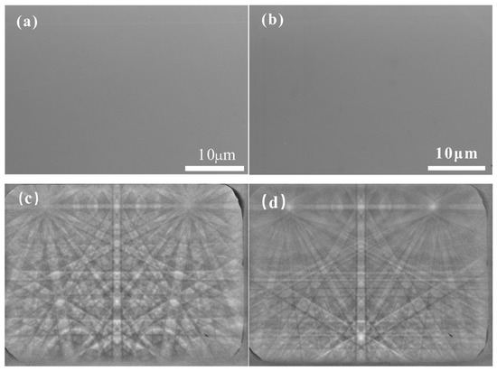
Figure 1.
Surface morphology of GaN grown with HVPE on (0001) 6H-SiC (a) and sapphire (b) substrates identified using SEM. EBSD Kikuchi patterns detected in the GaN (c) and the 6H-SiC substrate (d) of the cross-section in this heteroepitaxial system.
The epitaxial growth of GaN exhibits specific crystallographic orientations depending on the type of substrate used. For GaN grown on the c-plane sapphire substrate, the in-plane crystallographic-orientation relationship revealed a 30° rotation, indicating that (1–210) of the GaN aligns with (10–10) of the sapphire substrate [26].
To determine the crystallographic-orientation relationship between GaN and the 6H-SiC substrate, cross-sectional EBSD measurements were conducted. EBSD utilizes Kikuchi patterns to identify the crystallographic orientation of crystalline or polycrystalline materials, and it can confirm the Miller index of the surface for single-crystal materials. The cross section of the GaN/6H-SiC heteroepitaxy system was indexed using Kikuchi patterns and EBSD mapping measurements.
The wurtzite structure GaN and 6H-SiC both belong to the hexagonal P63mc space group. Consequently, the Kikuchi patterns exhibited by the epitaxy film and the substrate exhibit hexagonal characteristics. Figure 1c,d display the Kikuchi patterns on the cross sectional surface of the heteroepitaxy system, which are notably distinct, indicating the flatness of the surfaces and the quality of the GaN crystal structure. Utilizing the HKL CHANNEL5 software, the crystallographic orientation was determined based on the Kikuchi patterns. The findings reveal that both GaN and the 6H-SiC substrate on the cross sectional surface exhibit (10–10) planes.
EBSD mapping measurements were conducted on the cross-section of both GaN and 6H-SiC to validate their crystallographic-orientation relationship. The polar figures were generated using the HKL CHANNEL5 software based on the mapping results. It was observed that the (10–10) plane of GaN (as shown in Figure 2a) and the (10–10) plane of 6H-SiC (as shown in Figure 2b) exhibit parallel alignment. Given that the 6H-SiC substrate employed for epitaxy is oriented along the (0001) plane, it follows that the (0001) plane of GaN is also parallel to the (0001) plane of 6H-SiC. This crystallographic-orientation relationship is depicted in Figure 2c.
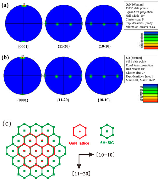
Figure 2.
The cross-sectional polar diagrams derived from the EBSD mapping of GaN (a) and the 6H-SiC substrate (b) within the heteroepitaxy system. A schematic representation elucidates the crystallographic-orientation relationship on the c-plane between GaN and the 6H-SiC substrate (c).
The lattice mismatch of the GaN/6H-SiC heteroepitaxy system was determined using the lattice parameters and the crystallographic-orientation relationship obtained from the EBSD results. Two methods were employed for this calculation [27,28]:
For our specific system, the lattice parameters are as follows: aepi = 0.3186 nm (GaN) [29] and asub = 0.3073 nm (6H-SiC) [30]. Consequently, the lattice mismatches were computed to be 3.7% and 3.5% using these two methods.
These findings deviate from the (0001) plane GaN/sapphire heteroepitaxy system, wherein the crystallographic-orientation relationship between the two materials involved a 30° angular rotation. This implies that the (1–210) plane of GaN aligns with the (10–10) plane of the sapphire substrate on the c-plane [26]. This phenomenon can be attributed to the differing lattice parameters and crystal structures of these materials. In the GaN/sapphire heteroepitaxial system, the sapphire substrate belongs to the R-3c space group. The in-plane crystallographic orientation leads to more N atoms of GaN aligning with the O atoms of the sapphire lattice when the GaN lattice rotates by 30° around the [0001] axis. Conversely, when the lattices are not rotated, the lattice mismatch was much larger, reducing the number of N atoms aligned with O atoms. Consequently, the average lattice mismatch increases, accompanied by increased atomic repulsions. In contrast, the GaN/6H-SiC heteroepitaxy system features lattice parameters and material symmetry that are more closely matched than the GaN/sapphire system. In this case, there is no need for GaN lattice rotation to match the 6H-SiC lattice in the (0001) plane. As a result, the lattice mismatch in the GaN/6H-SiC system is considerably smaller (3.7% and 3.5% for GaN/6H-SiC, compared to 16.1% and 13.8% for GaN/sapphire [26]). Consequently, the residual stress and dislocation density in GaN grown on the 6H-SiC substrate are significantly lower compared to those on the sapphire substrate due to the smaller mismatches in lattice parameters and thermal-expansion coefficients [20,21].
The actual heteroepitaxial structure does not strictly adhere to this orientation due to lattice mismatch. Some misorientation exists in the GaN crystal to accommodate the 6H-SiC substrate, particularly during the initial stages of growth. To assess the distribution of misorientation along the growth direction in different heteroepitaxial systems, EBSD mapping measurements were conducted on the cross-sectional surface near the interface between GaN and the foreign substrates (Figure 3). The reference direction was [0001], and the crystallographic orientation was collected using EBSD from Kikuchi diffraction patterns, yielding three Euler angles at each mapping point. The distribution of deviation from the [0001] direction of GaN epitaxy on 6H-SiC falls within the range of 2.5–4.5° (Figure 3a), while for GaN on the sapphire substrate, this range is 4.5–5.5° (Figure 3b). Larger deviation from the ideal growth direction implies greater lattice deformation, with strain being dependent on this deformation. The different deviation angles indicate that the lattice deformation of GaN epitaxy on sapphire is greater than that on the 6H-SiC substrate. EBSD mapping results for GaN on both 6H-SiC and sapphire demonstrate that deviation from the [0001] direction is greater near the interface and decreases with increasing GaN thickness. This trend aligns with the results obtained from z-axis mapping Raman spectrum measurements of GaN on various foreign substrates [20].
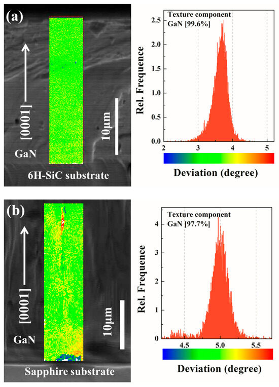
Figure 3.
The texture component results of GaN on 6H-SiC (a) and the sapphire substrate (b) near the interface of the heteroepitaxy system, as obtained from EBSD mapping data.
To assess the stress in GaN on these substrates, Raman spectroscopy was employed to determine the residual stress in the HVPE-GaN crystal. Raman spectrum details of HVPE GaN grown on 6H-SiC and sapphire substrates were shown in Table 1.The peak position of the E2(high) mode in the Raman spectrum is solely related to the stress within the GaN crystal. A previous publication indicated that a biaxial stress of 1 GPa causes a 4.2 cm−1 shift in the E2(high) Raman mode peak position [31], with the wavenumber of the stress-free GaN E2(high) Raman mode being 567.1 cm−1 [32]. Figure 4 presents the Raman spectra of GaN crystals grown on different foreign substrates. The E2(high) mode peak for GaN on the 6H-SiC substrate is found at 566.9 cm−1, while on the sapphire substrate, it is at 568.7 cm−1. The corresponding residual stress values for these peak positions are −0.047 GPa and 0.38 GPa, respectively. A positive value indicates compressive stress, while a negative value indicates tensile stress [33]. These results align with the findings of EBSD mapping and previous studies [20,21]. There are some reports that the Raman spectroscopy peak position and width of GaN are related to its dislocation density [34,35]. This phenomenon also shows a correlation between stress and dislocation of GaN. According to the Raman peaks’ details of GaN grown on different substrates and references, the dislocation density of GaN grown on SiC and sapphire substrates is in the order of approximately 108 cm−2. Dislocation and stress, as well as their impact on Raman spectroscopy, are complex and will be further studied in future work.

Table 1.
Raman spectrum details of HVPE GaN grown on 6H-SiC and sapphire substrates.
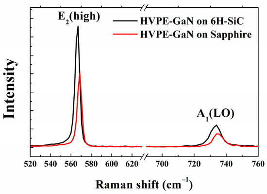
Figure 4.
The Raman spectra of the HVPE grown GaN crystals on the 6H-SiC and sapphire substrates.
Residual stress has an impact on the energy band gap of semiconductor materials. Different types of stress influence the energy band gap in opposite directions: tensile stress decreases it, while compressive stress increases it [36]. In photoluminescence spectra, the peak position of band-edge emission reflects the luminescent band gap. In this context, the PL peak position is influenced by the residual stress in the GaN crystal. Room temperature PL spectra of GaN crystals on 6H-SiC and sapphire substrates were obtained (Figure 5). The band-edge emission peak positions for these samples are 3.418 eV and 3.427 eV, respectively. A previous study reported a linear relationship with a linear coefficient of 21.1 meV/GPa for the luminescent band gap of GaN with respect to residual stress [36]. The difference in stress values for GaN on these substrates, calculated using this method, is 0.426 GPa, which is consistent with the Raman results (0.38 GPa + 0.047 GPa = 0.427 GPa). Additionally, the full width at half maximum (FWHM) of the band-edge emission peak for GaN on the 6H-SiC substrate is smaller than that on the sapphire substrate, indicating better crystal quality for GaN on 6H-SiC.
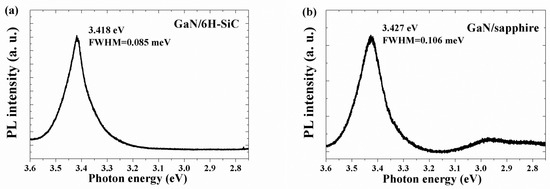
Figure 5.
The room-temperature photoluminescence spectra of the GaN crystals grown on the 6H-SiC (a) and sapphire substrate (b).
In order to determine the dislocation density of GaN crystals HVPE grown on different substrates, the HRXRD method was used to obtain their rocking curves. The broadening of symmetric and asymmetric diffraction peaks reflects the density of different types of dislocations in GaN crystals, respectively [37]. The HRXRD rocking curve results of GaN crystals are shown in Figure 6. The diffraction peaks full width’s half maximum (FWHM) of GaN crystals grown on SiC substrate is smaller than that on sapphire substrate (Table 2). Therefore, the HRXRD results indicate that the dislocation density and stress of GaN crystals grown on 6H-SiC substrates are lower than those on sapphire substrates. The dislocation density is calculated from HRXRD results in the order of approximately 108 cm−2. This is consistent with the Raman and PL results.
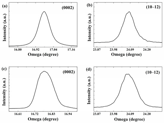
Figure 6.
HR-XRD rocking curves of HVPE GaN grown on the SiC substrate ((a) (0002) ω-scans and (b) (10–12) ω- scans) and sapphire substrate (c) (0002) ω-scans and (d) (10–12) ω- scans).

Table 2.
HRXRD rocking curve peak FWHM of HVPE GaN grown on 6H-SiC and sapphire substrates.
The mismatch between the 6H-SiC substrate and GaN crystal, arising from differences in lattice parameters and crystallographic orientation, is much smaller than that with the sapphire substrate. Consequently, the strain of GaN during the initial stages of epitaxy is strongly influenced by this mismatch. To optimize the growth conditions of GaN on different substrates, the stress and strain condition was assessed using Raman spectroscopy and EBSD. Adjustments to the growth conditions for GaN on various substrates were made based on the strain-distribution obtained from EBSD measurements, leading to the successful growth of GaN on the 6H-SiC substrate.
4. Conclusions
GaN crystals were successfully grown on MOCVD-GaN/sapphire and MOCVD-GaN/6H-SiC substrates using the HVPE method. The investigation into the crystallographic-orientation relationship utilized EBSD Kikuchi diffraction patterns and pole figures to analyze the GaN and 6H-SiC. It was observed that in the c-plane heteroepitaxy system, the (10–10) planes of GaN and 6H-SiC align parallel, a contrast to the GaN/sapphire heteroepitaxial system. When comparing the lattice mismatches, the ones between GaN and 6H-SiC substrates were found to be 3.7% and 3.5% using various calculation methods. These values are significantly lower than those observed for GaN grown on sapphire substrates. Furthermore, the deviation from the ideal growth direction of GaN is less pronounced on 6H-SiC than on sapphire substrates. The misorientation of GaN at the interface is highest and decreases progressively with growth on both 6H-SiC and sapphire substrates. Measurements from the Raman spectrum confirmed lower residual stress in GaN on 6H-SiC substrates compared to those on sapphire. The HRXRD results indicated that the dislocation density and stress of GaN crystal grown on 6H-SiC substrate are lower than on sapphire substrate. Additionally, the study of optical properties of GaN crystals on these substrates provided evidence supporting the observed stress conditions. This research enhances the understanding of crystallographic-orientation relationships and their effects on residual stress and optical properties in GaN crystals, offering insights for controlling crystal orientation in growing bulk GaN crystals on foreign substrates.
Author Contributions
X.H. and Y.W. designed the experiment. Y.S. wrote the main manuscript text. B.Z. and H.H. helped with the sample fabrication. All of the authors participated in the discussion and revision of the manuscript. All authors have read and agreed to the published version of the manuscript.
Funding
This research was supported by National Natural Science Foundation of China (Contract 11890702), Universities Twenty Foundational Items of Jinan City (2021GXRC039), Major innovation project for integrating science, education and industry of Qilu University of Technology (Shandong Academy of Sciences) (grant No. 2022JBZ01-07), Shandong Province’s Universities Young Innovative Talent Incubation Program—Wide Bandgap Semiconductor Materials Research Innovation Team, Qilu University of Technology Research Project (2022PY056), Shandong Provincial Natural Science Foundation (ZR2021QE255, ZR2021QE284, ZR2021QE175), and Taishan Scholar Program of Shandong Province (Xiaopeng Hao).
Data Availability Statement
Data are contained within the article.
Conflicts of Interest
The authors declare no conflict of interest.
References
- Iyer, P.P.; DeCrescent, R.A.; Mohtashami, Y.; Lheureux, G.; Butakov, N.A.; Alhassan, A.; Weisbuch, C.; Nakamura, S.; DenBaars, S.P.; Schuller, J.A. Unidirectional luminescence from InGaN/GaN quantum-well metasurfaces. Nat. Photonics 2020, 14, 543–548. [Google Scholar] [CrossRef]
- Benzarti, Z.; Sekrafi, T.; Bougrioua, Z.; Khalfallah, A.; El Jani, B. Effect of SiN Treatment on Optical Properties of InxGa1−xN/GaN MQW Blue LEDs. J. Electron. Mater. 2017, 46, 4312–4320. [Google Scholar] [CrossRef]
- Liang, F.; Zhao, D.G.; Liu, Z.S.; Chen, P.; Yang, J.; Duan, L.H.; Shi, Y.S.; Wang, H. GaN-based blue laser diode with 6.0 W of output power under continuous-wave operation at room temperature. J. Semicond. 2021, 42, 112801. [Google Scholar] [CrossRef]
- Hu, L.; Ren, X.Y.; Liu, J.P.; Tian, A.Q.; Jiang, L.R.; Huang, S.Y.; Zhou, W.; Zhang, L.Q.; Yang, H. High-power hybrid GaN-based green laser diodes with ITO cladding layer. Photonics Res. 2020, 3, 279–285. [Google Scholar] [CrossRef]
- Zhu, Y.X.; Liu, K.W.; Ai, Q.; Hou, Q.C.; Chen, X.; Zhang, Z.Z.; Xie, X.H.; Li, B.H.; Shen, D.Z. A high performance self-powered ultraviolet photodetector based on a p-GaN/n-ZnMgO heterojunction. J. Mater. Chem. C 2020, 8, 2719–2724. [Google Scholar] [CrossRef]
- Meneghini, M.; De Santi, C.; Abid, I.; Buffolo, M.; Cioni, M.; Khadar, R.A.; Nela, L.; Zagni, N.; Chini, A.; Medjdoub, F.; et al. GaN-based power devices: Physics, reliability, and perspectives. J. Appl. Phys. 2021, 130, 181101. [Google Scholar] [CrossRef]
- Kucharski, R.; Sochacki, T.; Lucznik, B.; Bockowski, M. Growth of bulk GaN crystals. J. Appl. Phys. 2020, 128, 050902. [Google Scholar] [CrossRef]
- Zhou, S.J.; Zhao, X.Y.; Du, P.; Zhang, Z.Q.; Liu, X.; Liu, S.; Guo, A. Application of patterned sapphire substrate for III-nitride light-emitting diodes. Nanoscale 2022, 14, 4887–4907. [Google Scholar] [CrossRef]
- Liu, F.; Zhang, Z.H.; Rong, X.; Yu, Y.; Wang, T.; Sheng, B.W.; Wei, J.Q.; Zhou, S.Y.; Yang, X.L.; Xu, F.J.; et al. Graphene-Assisted Epitaxy of Nitrogen Lattice Polarity GaN Films on Non-Polar Sapphire Substrates for Green Light Emitting Diodes. Adv. Funct. Mater. 2020, 30, 2001283. [Google Scholar] [CrossRef]
- Tang, D.S.; Qin, G.Z.; Hu, M.; Cao, B.Y. Thermal transport properties of GaN with biaxial strain and electron-phonon coupling. J. Appl. Phys. 2020, 127, 035102. [Google Scholar] [CrossRef]
- Boughrara, N.; Benzarti, Z.; Khalfallah, A.; Evaristo, M.; Cavaleiro, A. Comparative study on the nanomechanical behaviour and physical properties influenced by the epitaxial growth mechanisms of GaN thin films. Appl. Surf. Sci. 2022, 579, 152188. [Google Scholar] [CrossRef]
- Sharofidinov, S.S.; Kukushkin, S.A.; Red’kov, A.V.; Grashchenko, A.S.; Osipov, A.V. Growing III-V Semiconductor Heterostructures on SiC/Si Substrates. Tech. Phys. Lett. 2019, 45, 711–713. [Google Scholar] [CrossRef]
- Qiao, K.; Liu, Y.P.; Kim, C.; Molnar, R.J.; Osadchy, T.; Li, W.H.; Sun, X.C.; Li, H.S.; Myers-Ward, R.L.; Lee, D.; et al. Graphene Buffer Layer on SiC as a Release Layer for High-Quality Freestanding Semiconductor Membranes. Nano Lett. 2021, 21, 4013–4020. [Google Scholar] [CrossRef] [PubMed]
- Lin, M.E.; Swerdlov, B.G.; Zhou, L.; Morkoc, H. A comparative study of GaN epilayers grown on sapphire and SiC substrates by plasma-assisted molecular-beam epitaxy. Appl. Phys. Lett. 1993, 62, 3479–3481. [Google Scholar] [CrossRef]
- Yang, B.; Yang, H.Y.; Li, T.B.; Yang, J.M.; Yang, P. Thermal transport at 6H-SiC/graphene buffer layer/GaN heterogeneous interface. Appl. Surf. Sci. 2021, 536, 147828. [Google Scholar] [CrossRef]
- Saha, S.; Kumar, D.; Sharma, C.K.; Singh, V.K.; Channagiri, S.; Rao, D.V.S. Microstructural Characterization of GaN Grown on SiC. Microsc. Microanal. 2019, 25, 1383–1393. [Google Scholar] [CrossRef]
- Al Balushi, Z.Y.; Wang, K.; Ghosh, R.K.; Vilá, R.A.; Eichfeld, S.M.; Caldwell, J.D.; Qin, X.Y.; Lin, Y.C.; DeSario, P.A.; Stone, G.; et al. Two-dimensional gallium nitride realized via graphene encapsulation. Nat. Mater. 2016, 15, 1166–1171. [Google Scholar] [CrossRef]
- Kakanakova-Georgieva, A.; Ivanov, I.G.; Suwannaharn, N.; Hsu, C.W.; Cora, I.; Pécz, B.; Giannazzo, F.; Sangiovanni, D.G.; Gueorguiev, G.K. MOCVD of AlN on epitaxial graphene at extreme temperatures. CrystEngComm 2021, 23, 385–390. [Google Scholar] [CrossRef]
- Sangiovanni, D.G.; Faccio, R.; Gueorguiev, G.K.; Kakanakova-Georgieva, A. Discovering atomistic pathways for supply of metal atoms from methyl-based precursors to graphene surface. Phys. Chem. Chem. Phys. 2023, 25, 5887. [Google Scholar] [CrossRef]
- Zhang, L.; Shao, Y.L.; Hao, X.P.; Wu, Y.Z.; Qu, S.; Chen, X.F.; Xu, X.G. Comparison of the strain of GaN films grown on MOCVD-GaN/Al2O3 and MOCVD-GaN/SiC samples by HVPE growth. J. Cryst. Growth 2011, 334, 62–66. [Google Scholar] [CrossRef]
- Zhang, L.; Yu, J.X.; Hao, X.P.; Wu, Y.Z.; Dai, Y.B.; Shao, Y.L.; Zhang, H.D.; Tian, Y. Influence of stress in GaN crystals grown by HVPE on MOCVD-GaN/6H-SiC substrate. Sci. Rep. 2014, 4, 4179. [Google Scholar] [CrossRef] [PubMed]
- Yang, B.B.; Shi, C.Y.; Ye, X.J.; Teng, J.W.; Lai, R.L.; Cui, Y.J.; Guan, D.K.; Cui, H.W.; Li, Y.P.; Chiba, A. Underlying slip/twinning activities of Mg-xGd alloys investigated by modified lattice rotation analysis. J. Magnes. Alloys 2023, 11, 998–1015. [Google Scholar] [CrossRef]
- Naresh-Kumar, G.; Bruckbauer, J.; Winkelmann, A.; Yu, X.; Hourahine, B.; Edwards, P.R.; Wang, T.; Trager-Cowan, C.; Martin, R.W. Determining GaN Nanowire Polarity and its Influence on Light Emission in the Scanning Electron Microscope. Nano Lett. 2019, 19, 3863–3870. [Google Scholar] [CrossRef] [PubMed]
- Trager-Cowan, C.; Alasmari, A.; Avis, W.; Bruckbauer, J.; Edwards, P.R.; Ferenczi, G.; Hourahine, B.; Kotzai, A.; Kraeusel, S.; Kusch, G.; et al. Structural and luminescence imaging and characterisation of semiconductors in the scanning electron microscope. Semicond. Sci. Technol. 2020, 35, 054001. [Google Scholar] [CrossRef]
- Ruggles, T.J.; Deitz, J.I.; Allerman, A.A.; Carter, C.B.; Michael, J.R. Identification of Star Defects in Gallium Nitride with HREBSD and ECCI. Microsc. Microanal. 2021, 27, 257–265. [Google Scholar] [CrossRef]
- Shao, Y.L.; Dai, Y.B.; Hao, X.P.; Wu, Y.Z.; Zhang, L.; Zhang, H.D.; Tian, Y. EBSD crystallographic orientation research on strain distribution in hydride vapor phase epitaxy GaN grown on patterned substrate. CrystEngComm 2013, 15, 7965–7969. [Google Scholar] [CrossRef]
- Frank, F.C.; van der Merwe, J.H. One-Dimensional Dislocations. II Misfitting Monolayers; Proceedings of the Royal Society of London. Series A; Mathematical and physical sciences: London, UK, 1949; pp. 216–225. [Google Scholar]
- Matthews, J.W. Coherent interfaces and misfit dislocations. In Epitaxial Growth, Part B; Academic Press: New York, NY, USA, 1975; p. 560. [Google Scholar]
- Levinshtein, M.E.; Rumyantsev, S.L.; Shur, M.S. Properties of Advanced Semiconductor Materials GaN, AlN, InN, BN, SiC, SiGe; John Wiley & Sons, Inc.: Hoboken, NJ, USA, 2001; pp. 1–30. [Google Scholar]
- Shur, M.; Rumyantsev, S.; Levinshtein, M. SiC Materials and Devices, Volume 1; World Scientific: Hackensack, NJ, USA, 2006; pp. 43–76. [Google Scholar]
- Kisielowski, C.; Krüger, J.; Ruvimov, S.; Suski, T.; Ager, J.W., III; Jones, E.; Liliental-Weber, Z.; Rubin, M.; Weber, E.R.; Bremser, M.D.; et al. Strain-related phenomena in GaN thin films. Phys. Rev. B 1996, 54, 17745. [Google Scholar] [CrossRef]
- Goñi, A.R.; Siegle, H.; Syassen, K.; Thomsen, C.; Wagner, J.M. Effect of pressure on optical phonon modes and transverse effective charges in GaN and AlN. Phys. Rev. B 2001, 64, 035205. [Google Scholar] [CrossRef]
- Huang, Y.Q.; Liu, M.D.; Li, Z.; Zeng, Y.K.; Liu, S.B. Raman spectroscopy study of ZnO-based ceramic films fabricated by novel sol–gel process. Mater. Sci. Eng. B 2003, 97, 111–116. [Google Scholar] [CrossRef]
- Kitamura, T.; Nakashima, S.; Nakamura, N.; Furuta, K.; Okumura, H. Raman scattering analysis of GaN with various dislocation densities. Phys. Status Solidi-C 2008, 5, 1789–1791. [Google Scholar] [CrossRef]
- Nootz, G.; Schulte, A.; Chernyak, L.; Osinsky, A.; Jasinski, J.; Benamara, M.; Liliental-Weber, Z. Correlations between spatially resolved Raman shifts and dislocation density in GaN films. Appl. Phys. Lett. 2002, 80, 1355–1357. [Google Scholar] [CrossRef]
- Zhao, D.G.; Xu, S.J.; Xie, M.H.; Tong, S.Y.; Yang, H. Stress and its effect on optical properties of GaN epilayers grown on Si (111), 6H-SiC (0001), and c-plane sapphire. Appl. Phys. Lett. 2003, 83, 677–679. [Google Scholar] [CrossRef]
- Liu, J.Q.; Wang, J.F.; Liu, Y.F.; Huang, K.; Hu, X.J.; Zhang, Y.M.; Xu, Y.; Xu, K.; Yang, H. High-resolution X-ray diffraction analysis on HVPE-grown thick GaN layers. J. Cryst. Growth 2009, 311, 3080–3084. [Google Scholar] [CrossRef]
Disclaimer/Publisher’s Note: The statements, opinions and data contained in all publications are solely those of the individual author(s) and contributor(s) and not of MDPI and/or the editor(s). MDPI and/or the editor(s) disclaim responsibility for any injury to people or property resulting from any ideas, methods, instructions or products referred to in the content. |
© 2023 by the authors. Licensee MDPI, Basel, Switzerland. This article is an open access article distributed under the terms and conditions of the Creative Commons Attribution (CC BY) license (https://creativecommons.org/licenses/by/4.0/).