Article

First Demonstration of Extrinsic C-Doped Semi-Insulating N-Polar GaN Using Propane Precursor Grown on Miscut Sapphire Substrate by MOCVD

Electrical & Computer Engineering, University of Wisconsin-Madison, Madison, WI 53706, USA
*
Author to whom correspondence should be addressed.
Crystals 2023, 13(10), 1457; https://doi.org/10.3390/cryst13101457
Submission received: 31 August 2023 / Revised: 16 September 2023 / Accepted: 19 September 2023 / Published: 1 October 2023
(This article belongs to the Special Issue III-Nitride Materials: Properties, Growth, and Applications)

Abstract

:
In this study, carbon-doped semi-insulating N-polar GaN on a sapphire substrate was prepared using a propane precursor. Controlling the deposition rate of N-polar GaN helped to improve the carbon incorporation efficiency, providing a semi-insulating behavior. The material quality and surface roughness of the N-polar GaN improved with modified deposition conditions. C-doping using 1.8 mmol/min of propane gave an abrupt doping profile near the GaN/sapphire interface, which was useful for obtaining semi-insulating N-polar GaN grown on sapphire. This study shows that further development of the deposition process will allow for improved material quality and produce a state-of-the-art N-polar semi-insulating GaN layer.

1. Introduction

N-polar GaN-based high-electron-mobility transistors (HEMTs) show great potential as high-power (>5 W/mm) and high-frequency (W-band, 94 GHz) devices [1,2,3]. A parasitic conduction path other than the two-dimensional electron gas (2DEG) and high buffer leakage can potentially restrict the high-power operation of these transistors. A semi-insulating (S.I.) buffer layer is necessary for HEMT devices to increase the breakdown voltage while preventing leakage current and RF loss. The presence of residual oxygen in the deposition chamber, acting as a shallow donor, makes it non-trivial to achieve a semi-insulating (S.I.) GaN layer via the metal-organic chemical vapor deposition (MOCVD) deposition process [4]. In N-polar GaN, the incorporation of oxygen (O) is almost two orders of magnitude higher than that in Ga-polar GaN, which makes it challenging to obtain semi-insulating behavior [5,6,7,8,9]. Some methods for growing an S.I. GaN layer involve doping with iron (Fe), manganese (Mn), magnesium (Mg), and carbon (C), acting as a deep-level compensating acceptor state within GaN [10,11,12,13,14,15].
The gettering process is also one of the ways to reduce the background O concentration by trapping it, but it requires ion implantation, which can degrade the material quality [16,17], increase the cost, and reduce the throughput during production [18]. So, this process is not used in this study; rather, in situ techniques such as doping are chosen for improved material quality and reduced cost of production.
Fe doping using ferrocene is widely accepted as a way of generating a deep-level compensating acceptor state for growing S.I. GaN buffer layers [19]. Omega-rocking curve XRD measurements from prior studies showed the high-quality Fe-doped (1.3 × 10¹⁹/cm3) S.I. Ga-polar GaN layer [19]. The full-width at half maximum (FWHM) of the omega-rocking curve was determined to be 253 and 481 arc-sec across (002) and (102) orientations of GaN, respectively [19]. The memory effect of Fe-doping in Ga-polar GaN is a well-known phenomenon (similar to that of Mn [12] and Mg [20] doping in Ga-polar GaN), where the doping profile of Fe cannot be turned off abruptly [19,21]. After switching off the Fe precursor during the deposition of GaN, the Fe tail (slow-turn-off) extends till 0.8–1 μm [19,21]. The memory effect of Fe doping limits its applicability in HEMTs as Fe can also act as deep-level buffer traps that can potentially cause dispersive or current collapse effects in high-power RF amplifiers [10,19]. Heikman et al. showed a slow solid-phase incorporation effect of Fe-doping in Ga-polar GaN [21] and, because of that, the compensation of unintentional oxygen (O) incorporation at GaN/sapphire interface becomes non-trivial [22]. This problem becomes worse due to the higher-temperature nucleation of N-polar GaN compared to Ga-polar GaN [23], where the O concentration at the GaN/sapphire interface becomes larger compared to Ga-polar GaN. Alternatively, C-doping can help to reduce the background carrier concentration (O) while maintaining an abrupt doping profile, which is beneficial for HEMTs. C-doping can be achieved by the intrinsic doping method by utilizing the methyl (CH3) or ethyl (C2H5) group from the metal-organic precursors of gallium, such as Trimethyl-gallium (TMGA) or Triethyl-gallium (TEGa). Intrinsic C-doping can be obtained using modified process parameters such as deposition temperature, flow rate of TMGa or TEGa, reactor pressure, and V/III ratio. Another method for C-doping is extrinsic doping, which uses hydrocarbon precursors during deposition [24]. However, the most optimized deposition conditions for efficient intrinsic doping typically result in a 40–67% increase in the dislocation/defect density [10,24,25]. Hence, hydrocarbons like propane, ethylene, and iso-butane are favored as C-dopants, providing the flexibility to utilize optimized GaN deposition conditions while maintaining precise control over extrinsic carbon incorporation [24].
Shan Wu et al. [26] reported that background hydrogen [H] can affect the electrical properties of intrinsically C-doped Ga-polar GaN by forming C-H complexes. However, the same group has also shown that extrinsic C-doping using propane attracts 75% less H, thereby reducing the chance of the formation of C-H complexes [27]. Additionally, Fichtenbaum reported a background H concentration of 1.5 × 10¹⁷/cm3 in an N-polar GaN film grown on a miscut sapphire substrate [28]. It exhibits a deposition rate (~50 nm/min) similar to that in this study. So, in this study, only the C and O concentrations in the N-polar GaN were measured using the SIMS, as the H concentration in propane-doped semi-insulating N-polar GaN might not have significantly influenced the material and electrical properties compared to the concentrations of C and O.
In this study, we used propane as a source of carbon precursor for obtaining the S.I. N-polar GaN layer on the miscut sapphire substrate using a metal–organic chemical vapor deposition (MOCVD) reactor. As per the authors’ knowledge, this is the first attempt to demonstrate a C-doped S.I. The N-polar GaN layer with propane as a hydrocarbon precursor showed minimal deterioration (10–20% higher FWHM of the omega-rocking curve compared to the state-of-the-art curve) of the crystalline properties [29]. The incorporation efficiency of propane was improved in the N-polar GaN epitaxial layer under optimized deposition conditions. The main purpose of this study was to show the incorporation of carbon into N-polar GaN using propane as a gaseous precursor.

2. Experimental Methods

Propane-doped N-polar GaN was deposited on a miscut sapphire substrate using the MOCVD deposition technique. Trimethylgallium (TMGa) and ammonia (NH3) were used as group-III and group-V precursors, respectively. Propane was used as a carbon (C) dopant, and H2 was used as a carrier gas. The miscut sapphire sample was heated at 1300 °C, and nitridation was performed prior to the deposition of a high-temperature (1145 °C) nucleation layer at a reactor chamber pressure of 100 mbar and a V/III ratio of ~8000, similar to that mentioned by Keller et al. [23]. After that, 50 nm unintentionally doped (UID) N-polar GaN followed by 1.75 μm thick UID or propane-doped N-polar GaN was deposited at a high temperature (HT) of 1270 °C. Two different deposition conditions were used for the propane doping experiments in the 1.75 μm thick UID or propane-doped layer, where the TMGa molar flow was varied to observe the propane incorporation. For the first deposition condition (G1), 137 μmol/min TMGa was used with propane concentrations of 0 to 3.6 mmol/min. The second deposition condition (G2) had an increased TMGa molar flow of 204 μmol/min, and the propane concentration varied from 0 to 2.4 mmol/min. The propane flow did not increase to 3.6 mmol/min with G2 as semi-insulating behavior was obtained before 2.4 mmol/min. The V/III ratio was fixed for both G1 and G2. The deposition conditions and corresponding propane concentrations used for G1 and G2 are listed in Table 1.
The background electron concentration of all the samples was determined by Hall measurement using the Van der Pauw geometry. The omega-rocking curve was measured using a Panalytical Empyrean high-resolution X-ray diffraction (XRD) tool (Malvern Panalytical, Malvern, UK) for analyzing the material quality. The surface roughness of the deposited samples was measured using a Bruker Icon atomic force microscope (AFM) (Bruker, Billerica, USA). Secondary ion-mass spectroscopy (SIMS) measurement was performed using a Cameca instrument (Cameca, Gennevilliers, France) for measuring the O and C concentrations in the samples using Cs+ ions. All the samples showed hillock-free atomically smooth surfaces under a Nomarski optical microscope (Nikon, Minato, Japan).

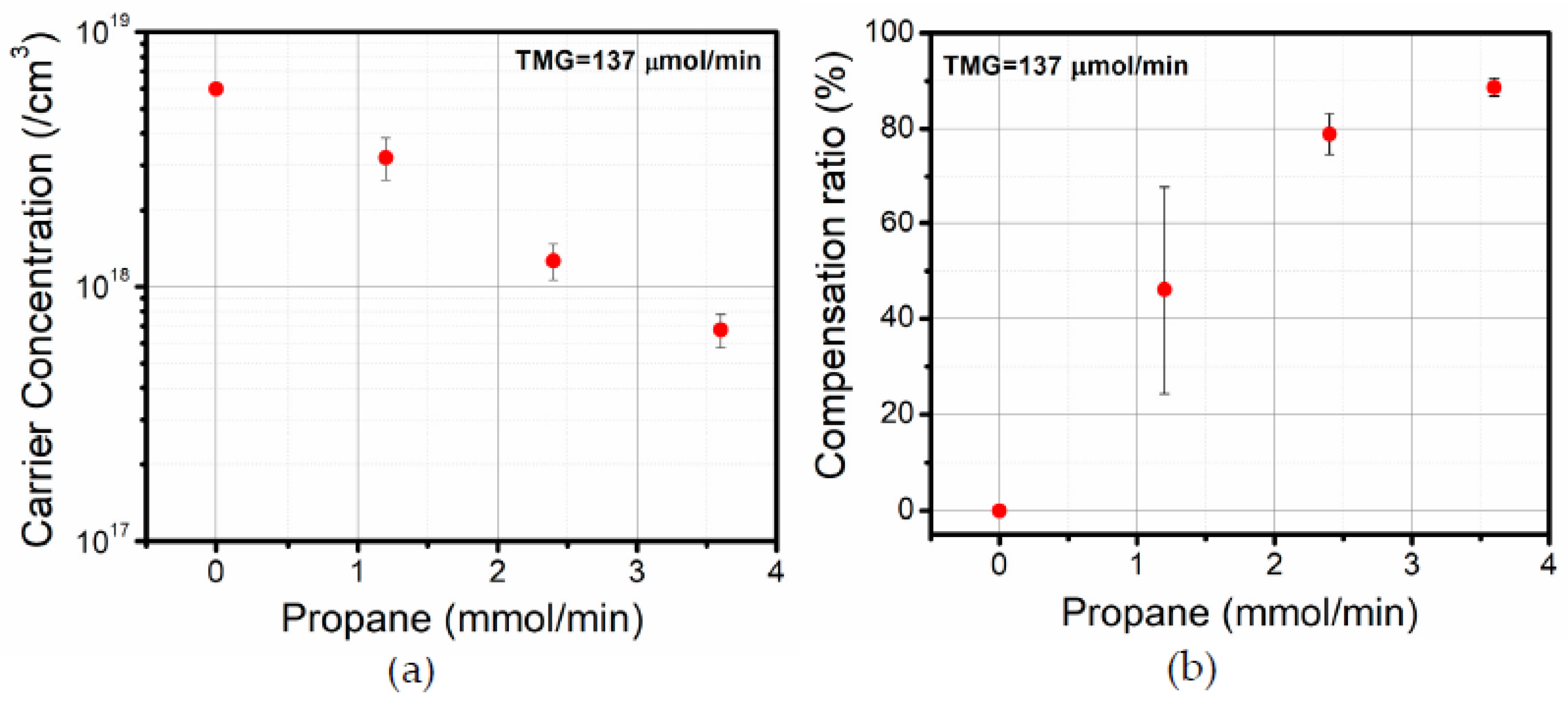
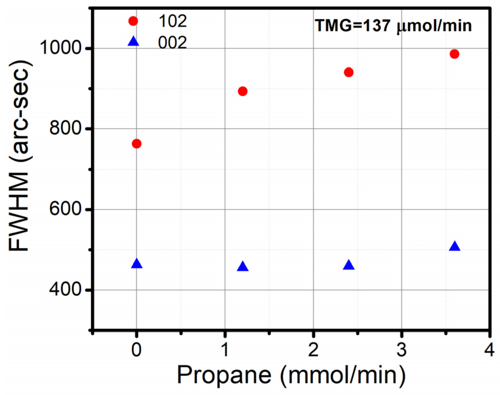
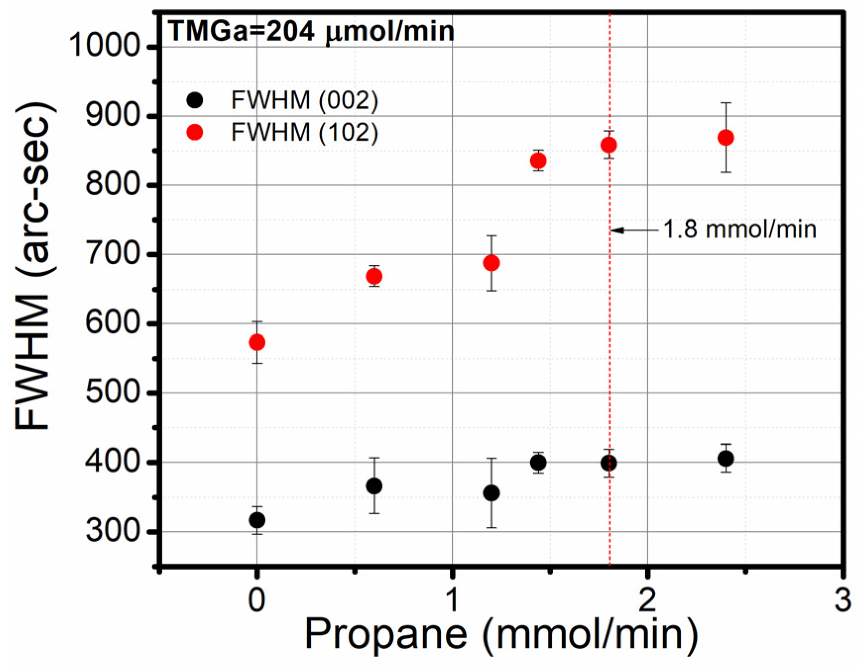
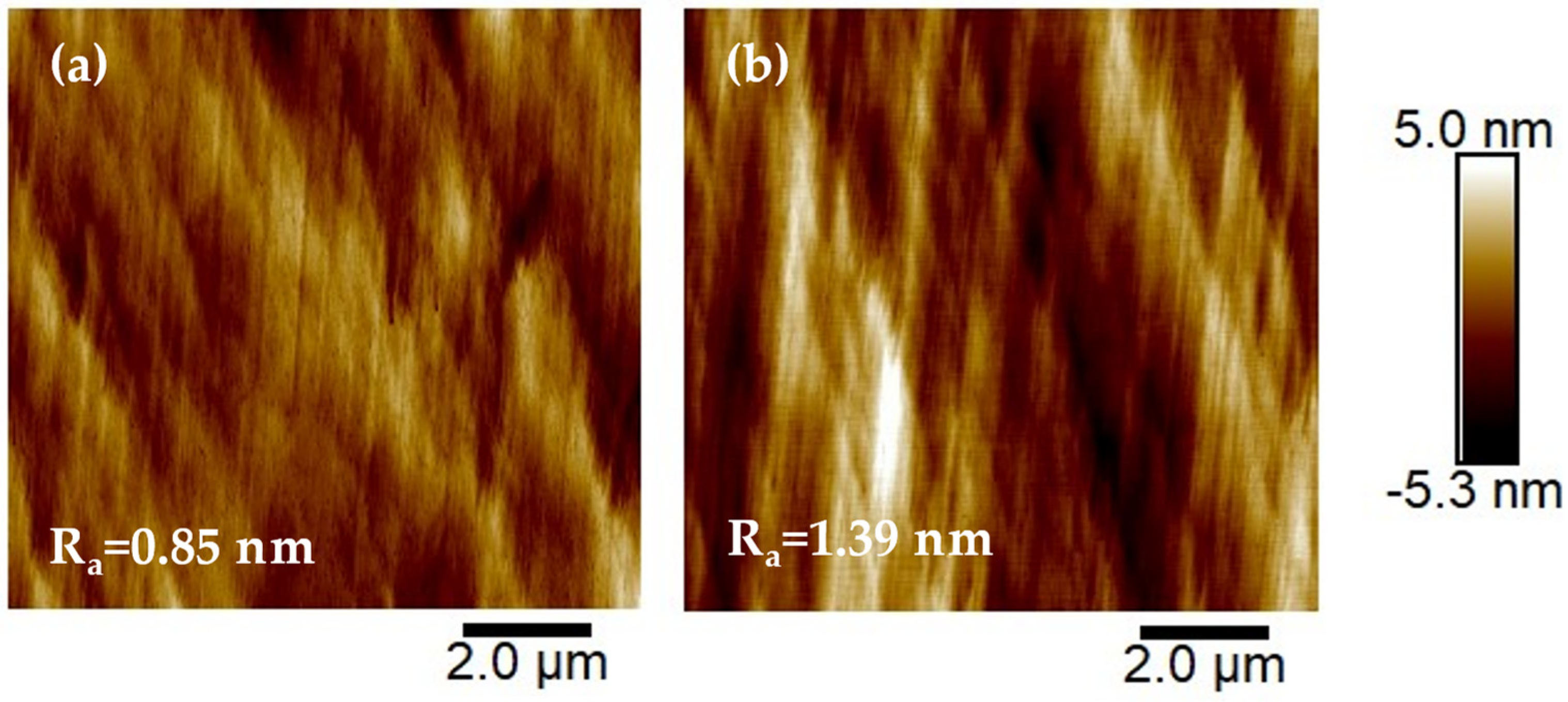
3. Results and Discussion

The carbon incorporation efficiency was primarily determined using Hall measurements. The first deposition condition (G1) with a TMGa flow rate of 137 μmol/min showed an exponential decay in the background carrier concentration with an increasing propane flow rate (Figure 1a). It was observed in the literature that the carbon concentration in Ga-polar GaN linearly depends on the propane flow rate [30]. So, it was expected that with increasing propane flow, the background carrier concentration would decrease and the compensation ratio ( C R = n U I D n C d o p e d n U I D × 100 ) would increase linearly. It was also determined from our experiment in N-polar GaN that the CR followed an almost linear profile with the propane flow rate (Figure 1b). At a very high propane flow rate, there was a small deviation in the CR from linearity. This might be related to the increased dislocation density, as shown in Figure 2. An increase in the dislocation density can increase the background O incorporation, as observed by Szymanski et al. [9].
Omega-rocking curve measurements indicated that with increasing propane flow rate, the off-axis (102) full-width half maxima (FWHM) increased, suggesting an increased edge dislocation density (Figure 2). The on-axis (002) FWHM remained nearly the same. The surface roughness appeared to be more or less similar with an increasing propane flow rate (Figure 3), and the step flow deposition was not affected by the increased propane flow. The RMS roughness of these propane-doped N-polar GaN samples was found to be less than 1.5 nm. Next, in the G2 series, the optimized deposition condition was used to increase the C-incorporation efficiency, such that even with the use of a lower amount of propane, S.I. behavior could be obtained.
To improve the incorporation of C using a propane precursor, the G2 deposition condition was used in the following studies. According to Lundin et al. [25], an increased deposition rate of Ga-polar GaN helps to increase the incorporation efficiency of C into GaN. This phenomenon was also studied in this work to understand the behavior of propane incorporation in N-polar GaN. Increasing the TMGa flow rate from 137 to 204 μmol/min increased the deposition rate from 60 to 90 nm/min and showed not only higher propane incorporation but also a reduced background carrier concentration. This might be related to the trapping of more carbon atoms during the deposition while limiting C desorption and fewer chances for O incorporation due to the higher supersaturation condition [9,31]. Hall measurements showed S.I. behavior with propane concentration > 1.8 mmol/min (Figure 4a). An exponential decay in the background carrier concentration was observed with monotonically increasing propane flow. Simultaneously, the slope of the CR with respect to the propane flow increased significantly for G2 (Figure 4b), indicating a better incorporation efficiency of propane at a higher TMGa molar flow rate.
The omega-rocking curve measurement of the G2 sample showed similar trends as those of G1. The FWHM increased with an increasing propane flow rate. Although it followed a comparable trend, it exhibited notably lower (10–20%) FWHM values in contrast to G1, suggesting a reduced dislocation density in comparison to G1 (Figure 5). The implementation of the modified deposition condition G2 assisted in achieving a semi-insulating N-polar GaN material while utilizing a decreased propane flow rate. It improved the material’s crystalline quality while reducing the background carrier concentration, indicating that the compensation of O mainly occurs due to the increased incorporation efficiency of C atoms and not due to the increase in dislocation and defect density. The FWHM value of the semi-insulating C-doped N-polar GaN was still higher than that of N-polar UID GaN. However, Lundin et al. demonstrated that fully optimized deposition conditions in heavily (2 × 10¹⁹/cm3) propane-doped Ga-polar semi-insulating GaN can provide a very low FWHM of the omega-rocking curve of the (002) and (102) planes of ~250 arc-sec and ~320 arc-sec, respectively [25]. So, further development by optimizing the growth conditions, such as V/III ratio, growth rate of N-polar GaN, growth temperature, and reactor pressure, needs to be performed to improve the FWHM parameter of semi-insulating N-polar GaN.
The surface roughness remained below 1.5 nm for the 10 × 10 μm2 AFM scan area, indicating device quality propane doped S.I. N-polar GaN samples using propane flow of 1.8 mmol/min and 2.4 mmol/min (Figure 6).
The SIMS measurement carried out for the G2 deposition condition using 2.4 mmol/min propane flow shows more than one order of higher C-concentration compared to the O and Si impurity levels, demonstrating complete semi-insulating behavior (Figure 7). The detection levels of O, C, and Si are 1016/cm3, 5 × 10¹⁶/cm3, and 1016/cm3, respectively. Figure 7 also shows the abrupt doping profile of C at the GaN/sapphire interface, which is crucial for obtaining S.I. behavior. It is known from the literature that the background O level is almost 2–4 times higher at the GaN/sapphire interface compared to bulk GaN [32]. In order to compensate for the increased background O at the N-polar GaN/sapphire interface, the C concentration needs to be significantly high near the interface. In Figure 7, it can be observed that the doping concentration of C reaches nearly 2 × 10¹⁸/cm3 in the vicinity of the interface, effectively compensating the background O concentration. The increased O needs to be fully compensated for by C, or the region near the interface needs to be fully depleted to obtain the semi-insulating property of N-polar GaN. It is possible to achieve a semi-insulating property if the C concentration is sufficiently higher than the increased O concentration. One of the possible reasons for obtaining a semi-insulating behavior might be due to more than one order higher C concentration compared to the O concentration in the bulk N-polar GaN. This higher C concentration might be sufficient to fully compensate for the increased O level at the interface. Another possible reason might be that the higher O level is near the nucleation layer, and it is not fully electrically conductive. In the nucleation layer, the N-polar GaN film quality might not be as good as that of the bulk, which appears from the thin island growth method in the nucleation layer [23]. So, even though the O concentration is higher near the interface, it does not act like a fully conductive path. However, the resolution of the SIMS measurement tool is insufficient to capture the thickness (possibly less than 50 nm) of the N-polar GaN/sapphire interface, where elevated O levels might exist. To accurately understand the physics behind the compensation mechanism near the N-polar GaN/sapphire interface, an extensive study using energy-dispersive X-ray spectroscopy needs to be performed, which is currently beyond the scope of this study. As a result, obtaining an accurate estimation of the O concentration at the interface is challenging.

4. Conclusions

This study is the first demonstration of propane-doped semi-insulating N-polar GaN deposited on top of a sapphire substrate. It was observed that with a higher deposition rate of N-polar GaN, the C-incorporation efficiency increased. Improved surface morphology and material quality were obtained by increasing the TMGa molar flow rate while obtaining an S.I. behavior with a comparatively lower propane flow rate. A propane flow rate of 1.8 mmol/min resulted in S.I. N-polar GaN along with a minimal surface roughness of 0.85 nm, which was deposited using 204 μmol/min of TMGa. This signifies that further development of propane doping in N-polar GaN will lead to improved material quality and production of S.I. C-doped N-polar GaN with a controlled doping profile.

Author Contributions

Conceptualization, S.M., C.G. and S.S.P.; methodology, S.M., C.G. and S.S.P.; validation, S.M., C.G. and S.S.P.; formal analysis, S.M., C.G. and S.S.P.; investigation, S.M., C.G. and S.S.P.; resources, C.G. and S.S.P.; data curation, S.M., S.S. and G.W.; writing—original draft preparation, S.M.; writing—review and editing, S.M., C.G. and S.S.P.; visualization, S.M., C.G. and S.S.P.; supervision, C.G. and S.S.P.; project administration, C.G. and S.S.P.; funding acquisition, C.G. and S.S.P. All authors have read and agreed to the published version of the manuscript.

Funding

This study was funded by the Office of Naval Research: N00014-22-1-2267 and monitored by Paul Maki.

Data Availability Statement

The data that support the findings of this study are available from the corresponding authors upon reasonable request.

Conflicts of Interest

The authors declare no conflict of interest.

References

  1. Romanczyk, B.; Li, W.; Guidry, M.; Hatui, N.; Krishna, A.; Wurm, C.; Keller, S.; Mishra, U.K. N-Polar GaN-on-Sapphire Deep Recess HEMTs With High W-Band Power Density. IEEE Electron Device Lett. 2020, 41, 1633–1636. [Google Scholar] [CrossRef]
  2. Romanczyk, B.; Wienecke, S.; Guidry, M.; Li, H.; Ahmadi, E.; Zheng, X.; Keller, S.; Mishra, U.K. Demonstration of Constant 8 W/mm Power Density at 10, 30, and 94 GHz in State-of-the-Art Millimeter-Wave N-Polar GaN MISHEMTs. IEEE Trans. Electron Devices 2017, 65, 45–50. [Google Scholar] [CrossRef]
  3. Li, W.; Romanczyk, B.; Guidry, M.; Akso, E.; Hatui, N.; Wurm, C.; Liu, W.; Shrestha, P.; Collins, H.; Clymore, C.; et al. Record RF Power Performance at 94 GHz From Millimeter-Wave N-Polar GaN-on-Sapphire Deep-Recess HEMTs. IEEE Trans. Electron Devices 2023, 70, 2075–2080. [Google Scholar] [CrossRef]
  4. Chung, B.-C.; Gershenzon, M. The influence of oxygen on the electrical and optical properties of GaN crystals grown by metalorganic vapor phase epitaxy. J. Appl. Phys. 1992, 72, 651–659. [Google Scholar] [CrossRef]
  5. Fichtenbaum, N.; Mates, T.; Keller, S.; DenBaars, S.; Mishra, U. Impurity incorporation in heteroepitaxial N-face and Ga-face GaN films grown by metalorganic chemical vapor deposition. J. Cryst. Growth 2008, 310, 1124–1131. [Google Scholar] [CrossRef]
  6. Tanikawa, T.; Kuboya, S.; Matsuoka, T. Control of impurity concentration in N-polar (0001¯) GaN grown by metalorganic vapor phase epitaxy. Phys. Status Solidi (b) 2017, 254, 1600751. [Google Scholar] [CrossRef]
  7. Tavernier, P.; Margalith, T.; Williams, J.; Green, D.; Keller, S.; DenBaars, S.; Mishra, U.; Nakamura, S.; Clarke, D. The growth of N-face GaN by MOCVD: Effect of Mg, Si, and In. J. Cryst. Growth 2004, 264, 150–158. [Google Scholar] [CrossRef]
  8. Sumiya, M.; Yoshimura, K.; Ohtsuka, K.; Fuke, S. Dependence of impurity incorporation on the polar direction of GaN film growth. Appl. Phys. Lett. 2000, 76, 2098–2100. [Google Scholar] [CrossRef]
  9. Szymanski, D.; Wang, K.; Kaess, F.; Kirste, R.; Mita, S.; Reddy, P.; Sitar, Z.; Collazo, R. Systematic oxygen impurity reduction in smooth N-polar GaN by chemical potential control. Semicond. Sci. Technol. 2022, 37, 015005. [Google Scholar] [CrossRef]
  10. Li, X.; Bergsten, J.; Nilsson, D.; Danielsson, Ö.; Pedersen, H.; Rorsman, N.; Janzén, E.; Forsberg, U. Carbon doped GaN buffer layer using propane for high electron mobility transistor applications: Growth and device results. Appl. Phys. Lett. 2015, 107, 262105. [Google Scholar] [CrossRef]
  11. Amilusik, M.; Zajac, M.; Sochacki, T.; Lucznik, B.; Fijalkowski, M.; Iwinska, M.; Wlodarczyk, D.; Somakumar, A.K.; Suchocki, A.; Bockowski, M. Carbon and Manganese in Semi-Insulating Bulk GaN Crystals. Materials 2022, 15, 2379. [Google Scholar] [CrossRef]
  12. Yamamoto, T.; Sazawa, H.; Nishikawa, N.; Kiuchi, M.; Ide, T.; Shimizu, M.; Inoue, T.; Hata, M. Reduction in Buffer Leakage Current with Mn-Doped GaN Buffer Layer Grown by Metal Organic Chemical Vapor Deposition. Jpn. J. Appl. Phys. 2013, 52, 08JN12. [Google Scholar] [CrossRef]
  13. Reshchikov, M.A.; Ghimire, P.; Demchenko, D.O. Magnesium acceptor in gallium nitride. I. Photoluminescence from Mg-doped GaN. Phys. Rev. B 2018, 97, 205204. [Google Scholar] [CrossRef]
  14. Hautakangas, S.; Oila, J.; Alatalo, M.; Saarinen, K.; Liszkay, L.; Seghier, D.; Gislason, H.P. Vacancy Defects as Compensating Centers in Mg-Doped GaN. Phys. Rev. Lett. 2003, 90, 137402. [Google Scholar] [CrossRef]
  15. Nakamura, S.; Iwasa, N.; Senoh, M.S.M.; Mukai, T.M.T. Hole Compensation Mechanism of P-Type GaN Films. Jpn. J. Appl. Phys. 1992, 31, 1258. [Google Scholar] [CrossRef]
  16. Ronning, C.; Carlson, E.P.; Thomson, D.B.; Davis, R.F. Optical activation of Be implanted into GaN. Appl. Phys. Lett. 1998, 73, 1622–1624. [Google Scholar] [CrossRef]
  17. Kucheyev, S.; Williams, J.; Pearton, S. Ion implantation into GaN. Mater. Sci. Eng. R Rep. 2001, 33, 51–108. [Google Scholar] [CrossRef]
  18. Majid, A.; Ali, A.; Zhu, J.; Wang, Y.; Yang, H. An evidence of defect gettering in GaN. Phys. B Condens. Matter 2008, 403, 2495–2499. [Google Scholar] [CrossRef]
  19. Heikman, S.; Keller, S.; DenBaars, S.P.; Mishra, U.K. Growth of Fe doped semi-insulating GaN by metalorganic chemical vapor deposition. Appl. Phys. Lett. 2002, 81, 439–441. [Google Scholar] [CrossRef]
  20. Xing, H.; Green, D.S.; Yu, H.; Mates, T.; Kozodoy, P.; Keller, S.; DenBaars, S.P.; Mishra, U.K. Memory Effect and Redistribution of Mg into Sequentially Regrown GaN Layer by Metalorganic Chemical Vapor Deposition. Jpn. J. Appl. Phys. 2003, 42, 50–53. [Google Scholar] [CrossRef]
  21. Heikman, S.; Keller, S.; Mates, T.; DenBaars, S.; Mishra, U. Growth and characteristics of Fe-doped GaN. J. Cryst. Growth 2003, 248, 513–517. [Google Scholar] [CrossRef]
  22. Heikman, S.J. MOCVD Growth Technologies for Applications in AlGaN/GaN High Electron Mobility Transistors. Ph.D. Thesis, University of California, Santa Barbara, CA, USA, September 2002. [Google Scholar]
  23. Keller, S.; Li, H.; Laurent, M.; Hu, Y.; Pfaff, N.; Lu, J.; Brown, D.F.; A Fichtenbaum, N.; Speck, J.S.; DenBaars, S.P.; et al. Recent progress in metal-organic chemical vapor deposition of (0001) N-Polar Group-III Nitrides. Semicond. Sci. Technol. 2014, 29, 113001. [Google Scholar] [CrossRef]
  24. Li, X.; Danielsson, Ö.; Pedersen, H.; Janzén, E.; Forsberg, U. Precursors for carbon doping of GaN in chemical vapor deposition. J. Vac. Sci. Technol. B 2015, 33, 021208. [Google Scholar] [CrossRef]
  25. Lundin, W.; Sakharov, A.; Zavarin, E.; Kazantsev, D.; Ber, B.; Yagovkina, M.; Brunkov, P.; Tsatsulnikov, A. Study of GaN doping with carbon from propane in a wide range of MOVPE conditions. J. Cryst. Growth 2016, 449, 108–113. [Google Scholar] [CrossRef]
  26. Wu, S.; Yang, X.; Zhang, Q.; Shang, Q.; Huang, H.; Shen, J.; He, X.; Xu, F.; Wang, X.; Ge, W.; et al. Direct evidence of hydrogen interaction with carbon: C–H complex in semi-insulating GaN. Appl. Phys. Lett. 2020, 116, 262101. [Google Scholar] [CrossRef]
  27. Wu, S.; Yang, X.; Wang, Z.; Ouyang, Z.; Huang, H.; Zhang, Q.; Shang, Q.; Shen, Z.; Xu, F.; Wang, X.; et al. Influence of intrinsic or extrinsic doping on charge state of carbon and its interaction with hydrogen in GaN. Appl. Phys. Lett. 2022, 120. [Google Scholar] [CrossRef]
  28. Fichtenbaum, N.A. Growth of Nitrogen-Face Gallium Nitride by MOCVD; Order No. 3330425; University of California: Santa Barbara, CA, USA, 2008. [Google Scholar]
  29. Bisi, D.; Romanczyk, B.; Liu, X.; Gupta, G.; Brown-Heft, T.; Birkhahn, R.; Lal, R.; Neufeld, C.J.; Keller, S.; Parikh, P.; et al. Commercially Available N-polar GaN HEMT Epitaxy for RF Applications. In Proceedings of the 2021 IEEE 8th Workshop on Wide Bandgap Power Devices and Applications (WiPDA), Redondo Beach, CA, USA, 7–11 November 2021; pp. 250–254. [Google Scholar] [CrossRef]
  30. Lesnik, A.; Hoffmann, M.P.; Fariza, A.; Bläsing, J.; Witte, H.; Veit, P.; Hörich, F.; Berger, C.; Hennig, J.; Dadgar, A.; et al. Properties of C-doped GaN. Phys. Status Solidi (b) 2016, 254, 1600708. [Google Scholar] [CrossRef]
  31. Seifert, W.; Franzheld, R.; Butter, E.; Sobotta, H.; Riede, V. On the origin of free carriers in high-conducting n-GaN. Cryst. Res. Technol. 1983, 18, 383–390. [Google Scholar] [CrossRef]
  32. Sumner, J.; Das Bakshi, S.; Oliver, R.A.; Kappers, M.J.; Humphreys, C.J. Unintentional doping in GaN assessed by scanning capacitance microscopy. Phys. Status Solidi (b) 2008, 245, 896–898. [Google Scholar] [CrossRef]
Figure 1. (a) Background carrier concentration and (b) compensation ratio of N-polar GaN deposited using G1 condition at different propane flow rates.
Crystals 13 01457 g001
Figure 2. FWHM of the omega-rocking curve, which was measured using HRXRD on propane-doped N-polar GaN samples grown using G1 deposition condition.
Crystals 13 01457 g002
Figure 3. AFM scans (10 μm×10 μm) of N-polar GaN samples growth under G1 deposition condition with propane concentration of (a) 0, (b) 1.2, (c) 2.4, and (d) 3.6 mmol/min.
Crystals 13 01457 g003
Figure 4. (a) Background carrier concentration and (b) compensation ratio of N-polar GaN at different propane flow rates.
Crystals 13 01457 g004
Figure 5. FWHM of the omega-rocking curve, measured using HRXRD on propane-doped N-polar GaN samples grown using G1 and G2 deposition conditions.
Crystals 13 01457 g005
Figure 6. AFM scans (10 μm × 10 μm) of N-polar GaN samples deposited using G2 deposition conditions at propane flow rates (a) 1.8 and (b) 2.4 mmol/min.
Crystals 13 01457 g006
Figure 7. SIMS measurement of propane-doped N-polar GaN sample with a propane flow rate of 2.4 mmol/min and deposition condition G2.
Crystals 13 01457 g007
Table 1. Deposition conditions along with the propane flow rate applied for the deposition of N-polar GaN.
Deposition ConditionTMGa Flow Rate (μmol/Min)Propane Flow Rate (mmol/Min)
G11370
1.2
2.4
3.6
G22040
0.6
1.2
1.4
1.8
2.4
Disclaimer/Publisher’s Note: The statements, opinions and data contained in all publications are solely those of the individual author(s) and contributor(s) and not of MDPI and/or the editor(s). MDPI and/or the editor(s) disclaim responsibility for any injury to people or property resulting from any ideas, methods, instructions or products referred to in the content.

