
Polytypes of sp2-Bonded Boron Nitride

 ,
,  , , , , , , and
Abstract
:1. Introduction
2. The Many Shapes of BN: Polymorphism and Polytypism
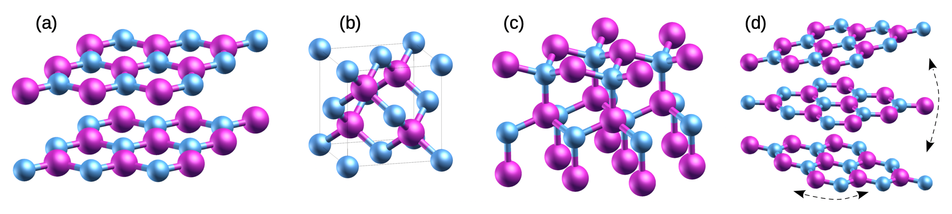
2.1. Polymorphisms
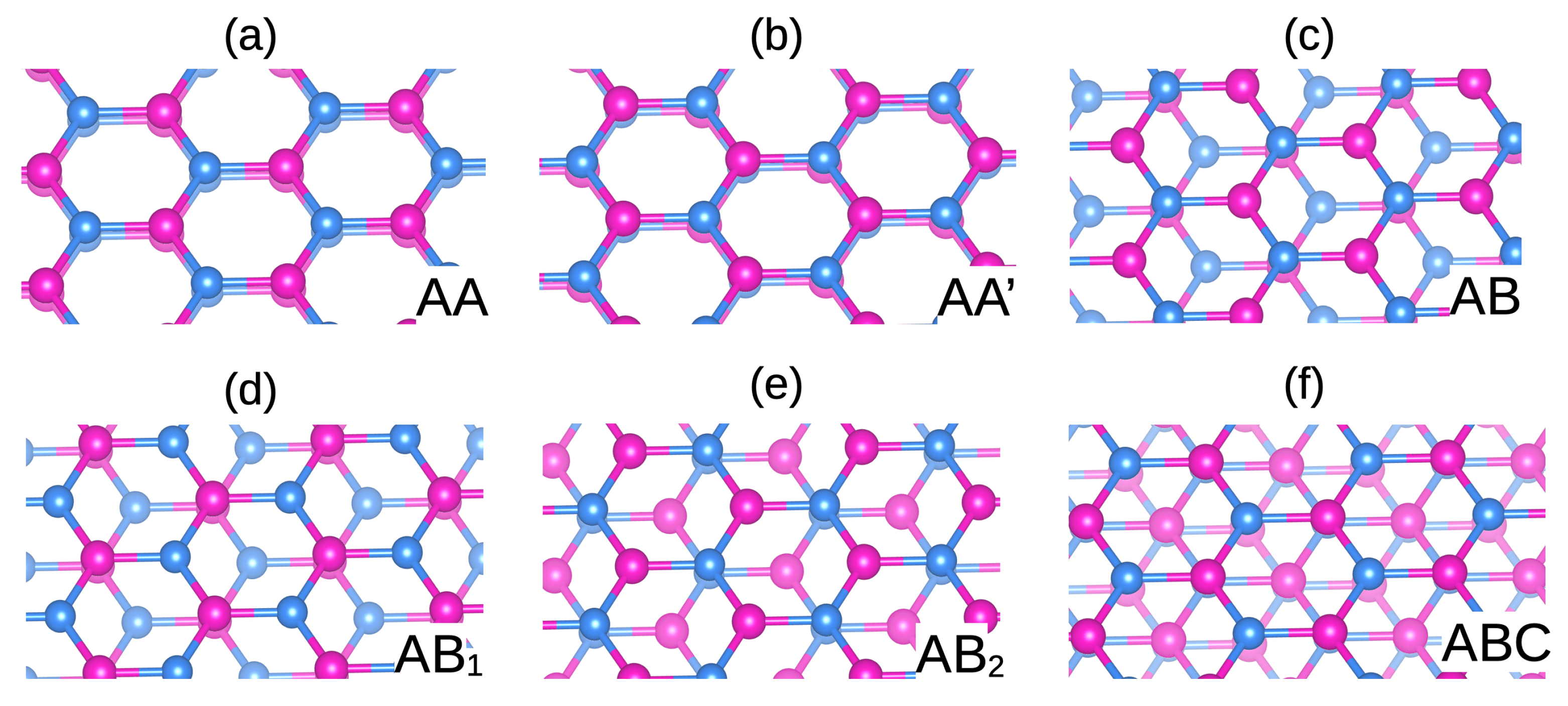
2.2. Polytypisms
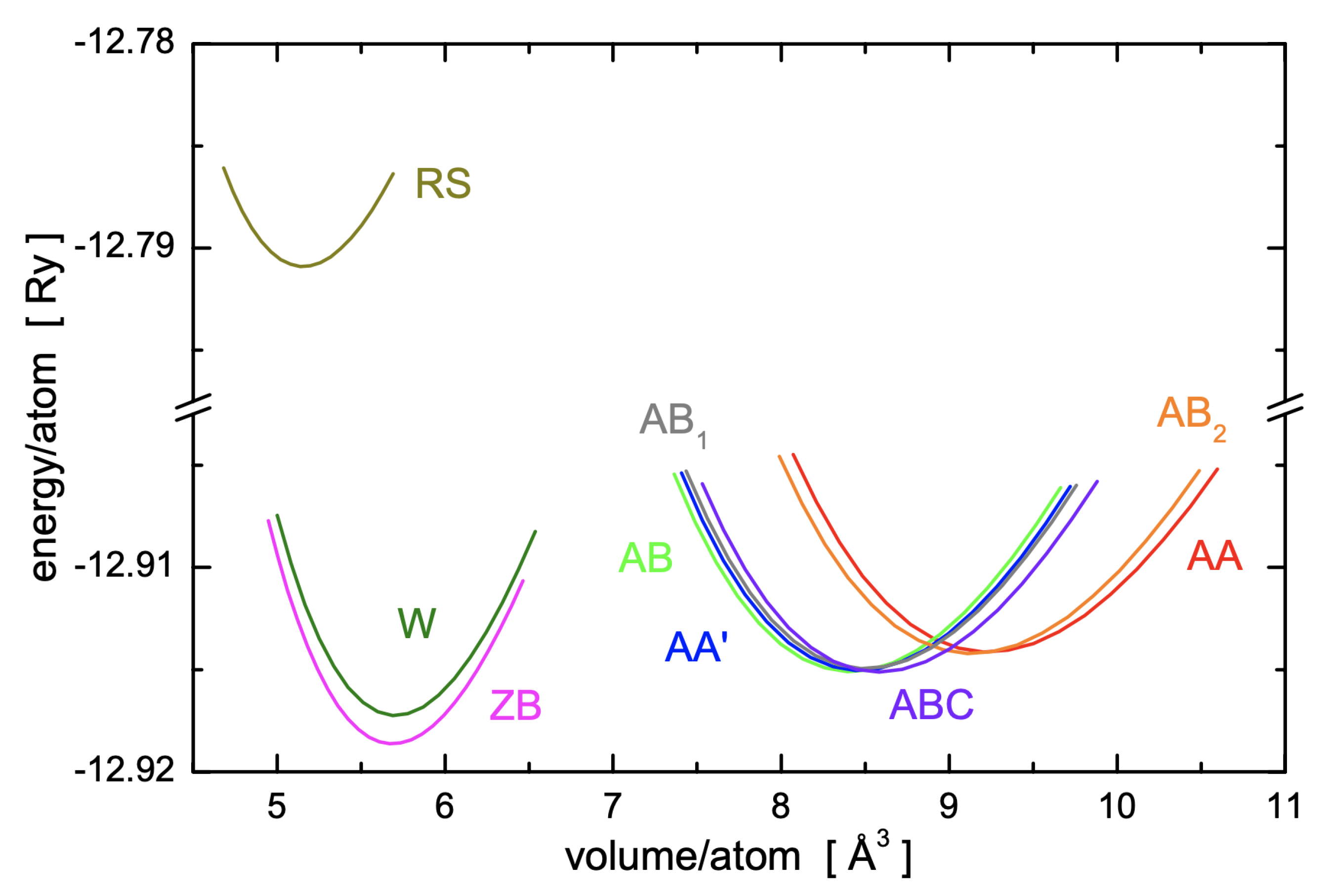
2.3. Crystal Cohesive Energies and Values of the Lattice Parameters
2.4. X-ray Diffraction Spectra for the Different Polytypes
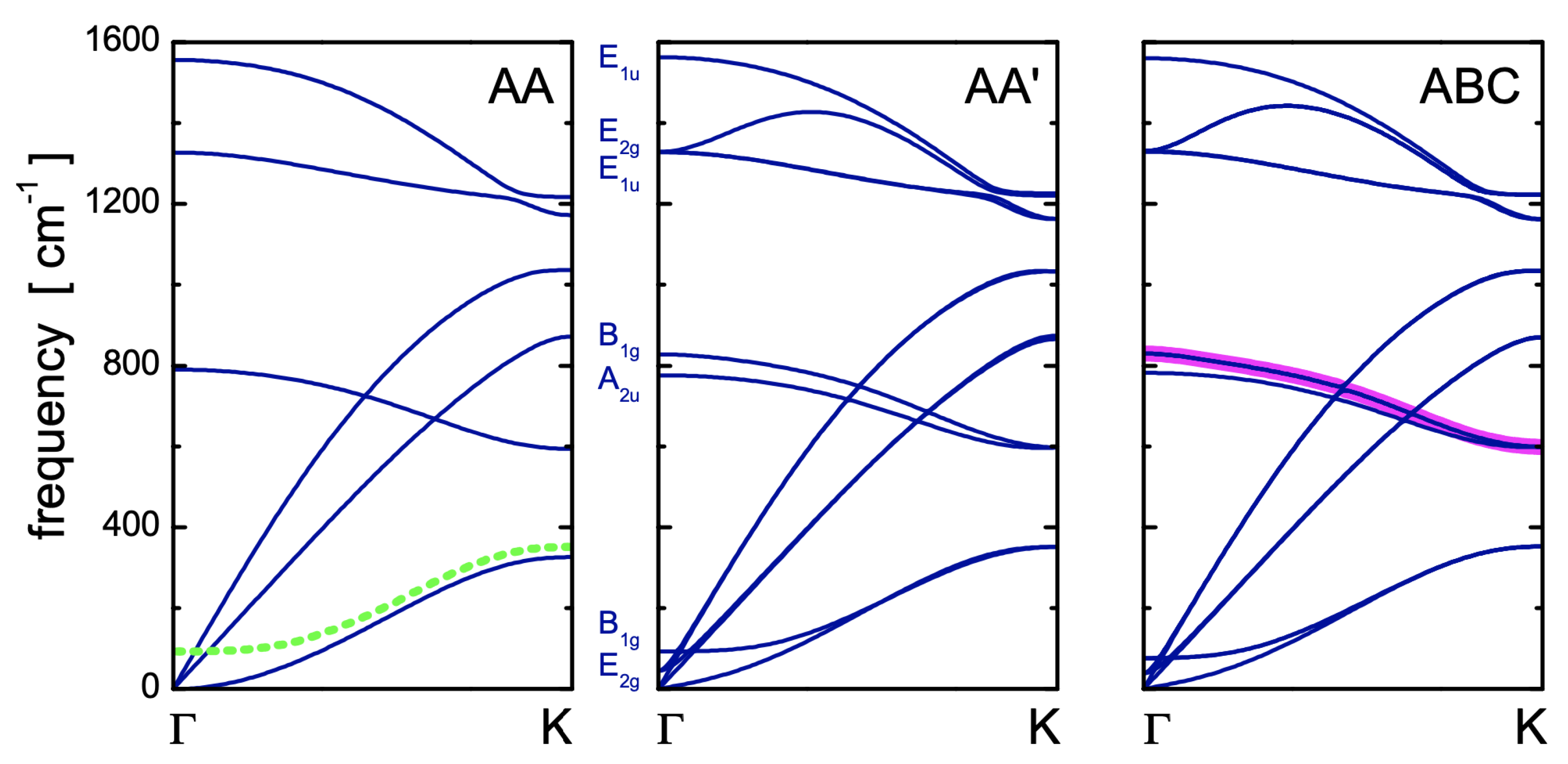
2.5. Symmetries and Dispersion Relations of Phonons for the Different Polytypes
2.6. Polytypism in Optical Experiments of the Early Days
3. The Optical Signatures of the Different Polytypes in the Deep Ultraviolet
3.1. Linear Optical Properties of hBN
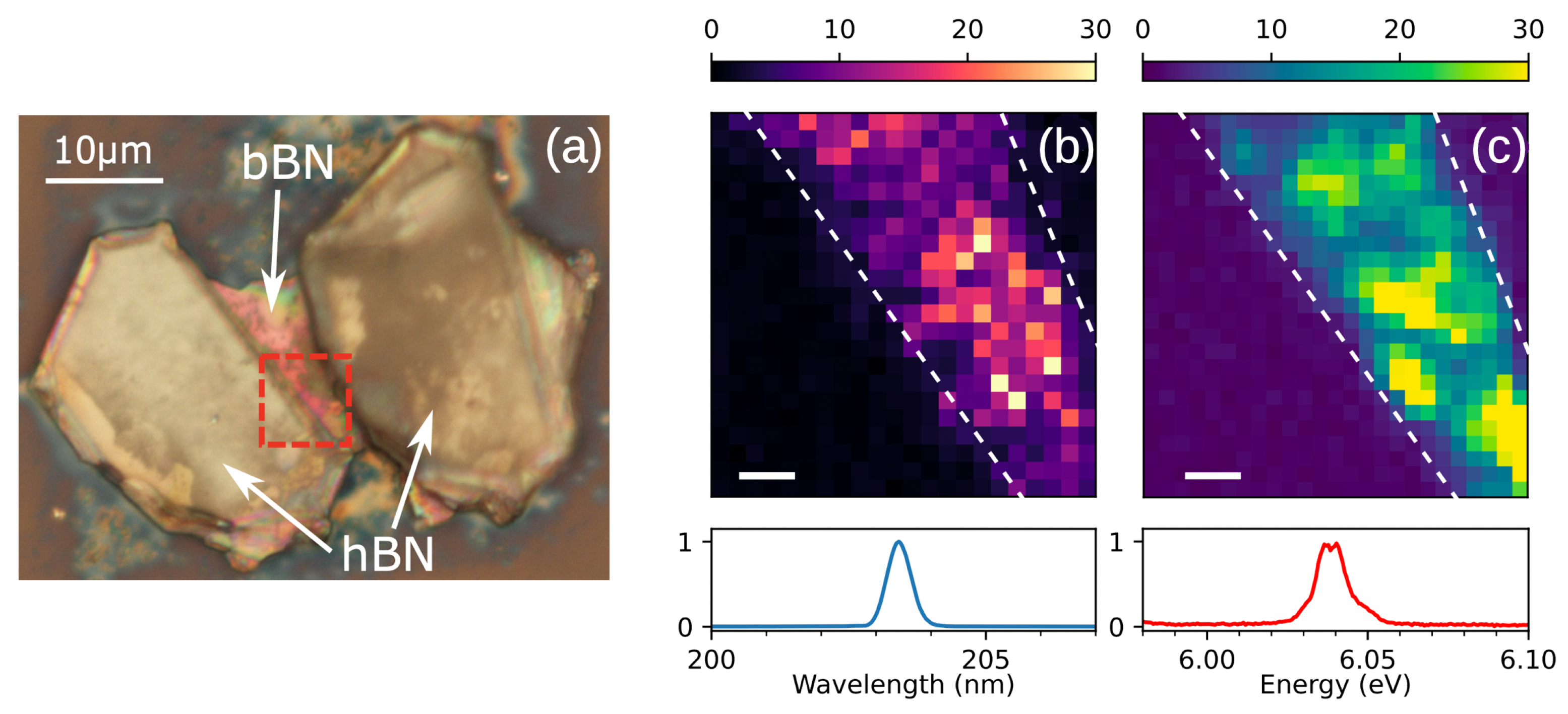
3.2. Linear Optical Properties of bBN
3.3. Linear Optical Properties of rBN
3.4. Linear Optical Properties of the BN Monolayer
3.5. Second Harmonic Generation in Some Polytypes
4. Conclusions
Author Contributions
Funding
Institutional Review Board Statement
Informed Consent Statement
Data Availability Statement
Acknowledgments
Conflicts of Interest
References
- Kneissl, M.; Seong, T.Y.; Han, J.; Amano, H. The emergence and prospects of deep-ultraviolet light-emitting diode technologies. Nat. Photonics 2019, 13, 233–244. [Google Scholar] [CrossRef]
- Nanishi, Y. The birth of the blue LED. Nat. Photonics 2014, 8, 884–886. [Google Scholar] [CrossRef]
- Kneissl, M.; Rass, J. (Eds.) III-Nitride Ultraviolet Emitters: Technology and Applications; Springer Series in Materials Science; Springer International Publishing: Cham, Switzerland, 2015; Volume 227. [Google Scholar] [CrossRef]
- Ueta, M.; Kanzaki, H.; Toyozawa, Y.; Hanamura, E. Handbook of Zinc Oxide and Related Materials; Springer: Berlin/Heidelberg, Germany, 1986; Volume 60. [Google Scholar] [CrossRef]
- Vuong, T.Q.P.; Lair, V.; Lacoste, F.R.; Halloumi, S.; Coindeau, S.; Thiel, J.; Shubina, T.V.; Pauthe, M.; Gil, B. Structural and Optical Properties of Zn1-xMgxO Prepared by Calcination of ZnO + Mg(OH)2 after Hydro Micro Mechanical Activation. Ann. Der Phys. 2019, 531, 1800379. [Google Scholar]
- Watanabe, K.; Taniguchi, T.; Kanda, H. Direct-bandgap properties and evidence for ultraviolet lasing of hexagonal boron nitride single crystal. Nat. Mater. 2004, 3, 404–409. [Google Scholar] [CrossRef]
- Watanabe, K.; Taniguchi, T.; Niiyama, T.; Miya, K.; Taniguchi, M. Far-ultraviolet plane-emission handheld device based on hexagonal boron nitride. Nat. Photonics 2009, 3, 591–594. [Google Scholar] [CrossRef]
- Bourrellier, R.; Meuret, S.; Tararan, A.; Stéphan, O.; Kociak, M.; Tizei, L.H.G.; Zobelli, A. Bright UV Single Photon Emission at Point Defects in h-BN. Nano Lett. 2016, 16, 4317–4321. [Google Scholar] [CrossRef]
- Su, C.; Zhang, F.; Kahn, S.; Shevitski, B.; Jiang, J.; Dai, C.; Ungar, A.; Park, J.H.; Watanabe, K.; Taniguchi, T.; et al. Tuning Color Centers at a Twisted Interface. arXiv 2021, arXiv:2108.04747v1. [Google Scholar]
- Caldwell, J.D.; Aharonovich, I.; Cassabois, G.; Edgar, J.H.; Gil, B.; Basov, D.N. Photonics with hexagonal boron nitride. Nat. Rev. Mater. 2019, 4, 552–567. [Google Scholar] [CrossRef]
- Baronnet, A. Some aspects of polytypism in crystals. Prog. Cryst. Growth Charact. 1978, 1, 151–211. [Google Scholar] [CrossRef]
- Pandey, D.; Krishna, P. The origin of polytype structures. Prog. Cryst. Growth Charact. 1983, 7, 213–258. [Google Scholar] [CrossRef]
- Mardix, S. Polytypism: A controlled thermodynamic phenomenon. Phys. Rev. B 1986, 33, 8677–8684. [Google Scholar] [CrossRef] [PubMed] [Green Version]
- Verma, A.; Krishna, P. Polymorphism and Polytypism in Crystals; John Wiley & Sons Inc.: New York, NY, USA, 1962. [Google Scholar]
- Balmain, W.H. Bemerkungen über die Bildung von Verbindungen des Bors und Siliciums mit Stickstoff und gewissen Metallen. J. Prakt. Chem. 1842, 27, 422–430. [Google Scholar] [CrossRef]
- Walther Bothe’s biography. Available online: https://en.wikipedia.org/wiki/Walther_Bothe (accessed on 17 March 2022).
- James Chadwick’s Biography. Available online: https://en.wikipedia.org/wiki/James_Chadwick (accessed on 4 May 2022).
- Henske, M.; Klein, M.; Köhli, M.; Lennert, P.; Modzel, G.; Schmidt, C.J.; Schmidt, U. The 10B based Jalousie neutron detector—An alternative for 3He filled position sensitive counter tubes. Nucl. Instruments Methods Phys. Res. Sect. Accel. Spectrometers Detect. Assoc. Equip. 2012, 686, 151–155. [Google Scholar] [CrossRef]
- Hassel, O. Die Krystallstruktur des bornitrides, BN. Norsk. Geol. Tidskr. 1926, 9, 266. [Google Scholar]
- Brager, A. An x-ray examination of the structure of boron nitride. Acta Physicochim. URSS 1937, 7, 699. [Google Scholar]
- Brager, A. An X-ray examination of titanium nitride III. Investigation by the powder method. Acta Physicochim. URSS 1939, 11, 617. [Google Scholar]
- Pease, R.S. Crystal Structure of Boron Nitride. Nature 1950, 165, 722–723. [Google Scholar] [CrossRef]
- Pease, R.S. An X-ray study of boron nitride. Acta Crystallogr. 1952, 5, 356–361. [Google Scholar] [CrossRef]
- Vuong, T.Q.P.; Cassabois, G.; Valvin, P.; Jacques, V.; Lee, A.V.D.; Zobelli, A.; Watanabe, K.; Taniguchi, T.; Gil, B. Phonon symmetries in hexagonal boron nitride probed by incoherent light emission. 2D Mater. 2016, 4, 11004. [Google Scholar] [CrossRef]
- Vuong, T.Q.P.; Liu, S.; Van der Lee, A.; Cuscó, R.; Artús, L.; Michel, T.; Valvin, P.; Edgar, J.H.; Cassabois, G.; Gil, B. Isotope engineering of van der Waals interactions in hexagonal boron nitride. Nat. Mater. 2018, 17, 152–158. [Google Scholar] [CrossRef] [Green Version]
- Liu, L.; Feng, Y.P.; Shen, Z.X. Structural and electronic properties of h-BN. Phys. Rev. B 2003, 68, 104102. [Google Scholar] [CrossRef]
- Coulson, C.A.; Taylor, R. Studies in Graphite and Related Compounds I: Electronic Band Structure in Graphite. Proc. Phys. Soc. Sect. A 1952, 65, 815–825. [Google Scholar] [CrossRef]
- Wentorf, R.H. Cubic Form of Boron Nitride. J. Chem. Phys. 1957, 26, 956. [Google Scholar] [CrossRef]
- Milledge, H.J.; Nave, E.; Weller, F.H. Transformation of Cubic Boron Nitride to a Graphitic Form of Hexagonal Boron Nitride. Nature 1959, 184, 715. [Google Scholar] [CrossRef]
- Zagyansky, L.; Samsonov, G.V. On the question of the oxidizability of boron nitride. J. Appl. Chem. USSR 1952, 25, 629. [Google Scholar]
- Corrigan, F.R.; Bundy, F.P. Direct transitions among the allotropic forms of boron nitride at high pressures and temperatures. J. Chem. Phys. 1975, 63, 3812–3820. [Google Scholar] [CrossRef]
- Xu, F.F.; Bando, Y.; Hasegawa, M. New phases of sp2-bonded boron nitride: The 12R and 24R polytypes. Chem. Commun. 2002, 14, 1490–1491. [Google Scholar] [CrossRef]
- Wentorf, R.H. Synthesis of the Cubic Form of Boron Nitride. J. Chem. Phys. 1961, 34, 809–812. [Google Scholar] [CrossRef]
- Narayan, J.; Bhaumik, A. Research Update: Direct conversion of h-BN into pure c-BN at ambient temperatures and pressures in air. APL Mater. 2016, 4, 20701. [Google Scholar] [CrossRef] [Green Version]
- Meng, Y.; Mao, H.K.; Eng, P.J.; Trainor, T.P.; Newville, M.; Hu, M.Y.; Kao, C.; Shu, J.; Hausermann, D.; Hemley, R.J. The formation of sp3 bonding in compressed BN. Nat. Mater. 2004, 3, 111–114. [Google Scholar] [CrossRef]
- Solozhenko, V.L. Thermodynamics of dense boron nitride modifications and a new phase P,T diagram for BN. Thermochim. Acta 1993, 218, 221–227. [Google Scholar] [CrossRef]
- Eremets, M.I.; Takemura, K.; Yusa, H.; Golberg, D.; Bando, Y.; Blank, V.D.; Sato, Y.; Watanabe, K. Disordered state in first-order phase transitions: Hexagonal-to-cubic and cubic-to-hexagonal transitions in boron nitride. Phys. Rev. B 1998, 57, 5655–5660. [Google Scholar] [CrossRef]
- Solozhenko, V.L.; Turkevich, V.Z.; Holzapfel, W.B. Refined Phase Diagram of Boron Nitride. J. Phys. Chem. B 1999, 103, 2903–2905. [Google Scholar] [CrossRef]
- Petrescu, M.I.; Balint, M.G. Structure and properties modifications in boron nitride. Part I: Direct polymorphic transformations mechanisms. UPB Sci. Bull. Ser. B 2007, 69, 35. [Google Scholar]
- Edgar, J.H.; Strite, S.; Akasaki, I.; Amano, H.; Wetzel, C. (Eds.) Properties of Group III Nitrides; EMIS Datareviews Series; INSPEC, Institution of Electrical Engineers: London, UK, 1994; Volume 23. [Google Scholar]
- Chilleri, J.; Siddiqua, P.; Shur, M.S.; O’Leary, S.K. Cubic boron nitride as a material for future electron device applications: A comparative analysis. Appl. Phys. Lett. 2022, 120, 122105. [Google Scholar] [CrossRef]
- Riter, J.R. Discussion of shock-induced graphite →wurtzite phase transformation in BN and implications for stacking in graphitic BN. J. Chem. Phys. 1973, 59, 1538. [Google Scholar] [CrossRef]
- Yixi, S.; Xin, J.; Kun, W.; Chaoshu, S.; Zhengfu, H.; Junyan, S.; Jie, D.; Sheng, Z.; Yuanbin, C. Vacuum-ultraviolet reflectance spectra and optical properties of nanoscale wurtzite boron nitride. Phys. Rev. B 1994, 50, 18637–18639. [Google Scholar] [CrossRef]
- Dubrovinskaia, N.; Solozhenko, V.L.; Miyajima, N.; Dmitriev, V.; Kurakevych, O.O.; Dubrovinsky, L. Superhard nanocomposite of dense polymorphs of boron nitride: Noncarbon material has reached diamond hardness. Appl. Phys. Lett. 2007, 90, 101912. [Google Scholar] [CrossRef]
- Wills, R.R. Wurtzitic boron nitride—A review. Int. J. High Technol. Ceram. 1985, 1, 139–153. [Google Scholar] [CrossRef]
- Kudrawiec, R.; Hommel, D. Bandgap engineering in III-nitrides with boron and group V elements: Toward applications in ultraviolet emitters. Appl. Phys. Rev. 2020, 7, 041314. [Google Scholar] [CrossRef]
- Chopra, N.G.; Luyken, R.J.; Cherrey, K.; Crespi, V.H.; Cohen, M.L.; Louie, S.G.; Zettl, A. Boron Nitride Nanotubes. Science 1995, 269, 966–967. [Google Scholar] [CrossRef] [PubMed]
- Chen, Y.I. (Ed.) Nanotubes and Nanosheets: Functionalization and Applications of Boron Nitride and Other Nanomaterials; CRC Press: Boca Raton, FL, USA, 2015. [Google Scholar]
- Baumhauer, H. Uber die Krystalle des Corborundums. Zeitshrift Kryst. Mineral. 1912, 50, 33. [Google Scholar]
- Baumhauer, H. Uber die verschiedenen Modifikationen des Carborundums und die Erscheinung der Polytypie. Zeitshrift Kryst. Mineral. 1915, 55, 249. [Google Scholar] [CrossRef] [Green Version]
- Jagodzinski, H. Polytypism in SiC crystals. Acta Crystallogr. 1954, 7, 300. [Google Scholar] [CrossRef]
- Frank, F.C. LXXXIII. Crystal dislocations—Elementary concepts and definitions. Lond. Edinb. Dublin Philos. Mag. J. Sci. 1951, 42, 809–819. [Google Scholar] [CrossRef]
- Moore, A.W. Characterization of pyrolytic boron nitride for semiconductor materials processing. J. Cryst. Growth 1990, 106, 6–15. [Google Scholar] [CrossRef]
- Thomas, J.; Weston, N.E.; O’Connor, T.E. Turbostratic Boron Nitride, Thermal Transformation to Ordered-layer-lattice Boron Nitride. J. Am. Chem. Soc. 1962, 84, 4619–4622. [Google Scholar] [CrossRef]
- Giannozzi, P.; Baroni, S.; Bonini, N.; Calandra, M.; Car, R.; Cavazzoni, C.; Ceresoli, D.; Chiarotti, G.L.; Cococcioni, M.; Dabo, I.; et al. QUANTUM ESPRESSO: A modular and open-source software project for quantum simulations of materials. J. Phys. Condens. Matter 2009, 21, 395502. [Google Scholar] [CrossRef]
- Giannozzi, P.; Andreussi, O.; Brumme, T.; Bunau, O.; Nardelli, M.B.; Calandra, M.; Car, R.; Cavazzoni, C.; Ceresoli, D.; Cococcioni, M.; et al. Advanced capabilities for materials modelling with Quantum ESPRESSO. J. Phys. Condens. Matter 2017, 29, 465901. [Google Scholar] [CrossRef] [Green Version]
- Xu, Y.N.; Ching, W.Y. Calculation of ground-state and optical properties of boron nitrides in the hexagonal, cubic, and wurtzite structures. Phys. Rev. B 1991, 44, 7787–7798. [Google Scholar] [CrossRef]
- Furthmuller, J.; Hafner, J.; Kresse, G. Ab initio calculation of the structural and electronic properties of carbon and boron nitride using ultrasoft pseudopotentials. Phys. Rev. B 1994, 50, 15606–15622. [Google Scholar] [CrossRef] [PubMed]
- Albe, K. Theoretical study of boron nitride modifications at hydrostatic pressures. Phys. Rev. B 1997, 55, 6203–6210. [Google Scholar] [CrossRef]
- Ohba, N.; Miwa, K.; Nagasako, N.; Fukumoto, A. First-principles study on structural, dielectric, and dynamical properties for three BN polytypes. Phys. Rev. B 2001, 63, 115207. [Google Scholar] [CrossRef]
- Ooi, N.; Rairkar, A.; Lindsley, L.; Adams, J.B. Electronic structure and bonding in hexagonal boron nitride. J. Phys. Condens. Matter. 2005, 18, 97–115. [Google Scholar] [CrossRef]
- Constantinescu, G.; Kuc, A.; Heine, T. Stacking in Bulk and Bilayer Hexagonal Boron Nitride. Phys. Rev. Lett. 2013, 111, 36104. [Google Scholar] [CrossRef]
- Silly, M.G.; Jaffrennou, P.; Barjon, J.; Lauret, J.S.; Ducastelle, F.; Loiseau, A.; Obraztsova, E.; Attal-Tretout, B.; Rosencher, E. Luminescence properties of hexagonal boron nitride: Cathodoluminescence and photoluminescence spectroscopy measurements. Phys. Rev. B 2007, 75, 85205. [Google Scholar] [CrossRef]
- Gao, S.P. Crystal structures and band gap characters of h-BN polytypes predicted by the dispersion corrected DFT and GW method. Solid State Commun. 2012, 152, 1817–1820. [Google Scholar] [CrossRef]
- Haga, T.; Matsuura, Y.; Fujimoto, Y.; Saito, S. Electronic states and modulation doping of hexagonal boron nitride trilayers. Phys. Rev. Mater. 2021, 5, 94003. [Google Scholar] [CrossRef]
- Kurdyumov, A.V.; Solozhenko, V.L.; Zelyavski, W.B. Lattice Parameters of Boron Nitride Polymorphous Modifications as a Function of Their Crystal-Structure Perfection. J. Appl. Crystallogr. 1995, 28, 540–545. [Google Scholar] [CrossRef]
- Chubarov, M.; Pedersen, H.; Hogberg, H.; Jensen, J.; Henry, A. Growth of High Quality Epitaxial Rhombohedral Boron Nitride. Cryst. Growth Des. 2012, 12, 3215–3220. [Google Scholar] [CrossRef]
- Chubarov, M.; Pedersen, H.; Hogberg, H.; Henry, A.; Czigány, Z. Initial stages of growth and the influence of temperature during chemical vapor deposition of sp2-BN films. J. Vac. Sci. Technol. A 2015, 33, 61520. [Google Scholar] [CrossRef] [Green Version]
- Chubarov, M.; Hogberg, H.; Henry, A.; Pedersen, H. Review Article: Challenge in determining the crystal structure of epitaxial 0001 oriented sp2-BN films. J. Vac. Sci. Technol. A 2018, 36, 30801. [Google Scholar] [CrossRef] [Green Version]
- Souqui, L.; Pedersen, H.; Hogberg, H. Thermal chemical vapor deposition of epitaxial rhombohedral boron nitride from trimethylboron and ammonia. J. Vac. Sci. Technol. A 2019, 37, 20603. [Google Scholar] [CrossRef]
- Yamada, H.; Kumagai, N.; Yamada, T.; Yamamoto, T. Dielectric functions of CVD–grown boron nitride from 1.1 to 9.0 eV by spectroscopic ellipsometry. Appl. Phys. Lett. 2021, 118, 112101. [Google Scholar] [CrossRef]
- Moret, M.; Rousseau, A.; Valvin, P.; Sharma, S.; Souqui, L.; Pedersen, H.; Hogberg, H.; Cassabois, G.; Li, J.; Edgar, J.H.; et al. Rhombohedral and turbostratic boron nitride: X-ray diffraction and photoluminescence signatures. Appl. Phys. Lett. 2021, 119, 262102. [Google Scholar] [CrossRef]
- Geick, R.; Perry, C.H.; Rupprecht, G. Normal Modes in Hexagonal Boron Nitride. Phys. Rev. 1966, 146, 543–547. [Google Scholar] [CrossRef]
- Babich, I.L. Raman spectrum of hexagonal boron nitride. Theor. Exp. Chem. 1974, 8, 594–595. [Google Scholar] [CrossRef]
- Kuzuba, T.; Era, K.; Ishii, T.; Sato, T. A low frequency Raman-active vibration of hexagonal boron nitride. Solid State Commun. 1978, 25, 863–865. [Google Scholar] [CrossRef]
- Kuzuba, T.; Sato, Y.; Yamaoka, S.; Era, K. Raman-scattering study of high-pressure effects on the anisotropy of force constants of hexagonal boron nitride. Phys. Rev. B 1978, 18, 4440–4443. [Google Scholar] [CrossRef]
- Nemanich, R.J.; Solin, S.A.; Martin, R.M. Light scattering study of boron nitride microcrystals. Phys. Rev. B 1981, 23, 6348–6356. [Google Scholar] [CrossRef]
- Cuscó, R.; Artús, L.; Edgar, J.H.; Liu, S.; Cassabois, G.; Gil, B. Isotopic effects on phonon anharmonicity in layered van der Waals crystals: Isotopically pure hexagonal boron nitride. Phys. Rev. B 2018, 97, 155435. [Google Scholar] [CrossRef] [Green Version]
- Cuscó, R.; Edgar, J.H.; Liu, S.; Cassabois, G.; Gil, B.; Artús, L. Influence of isotopic substitution on the anharmonicity of the interlayer shear mode of h-BN. Phys. Rev. B 2019, 99, 85428. [Google Scholar] [CrossRef] [Green Version]
- Cuscó, R.; Edgar, J.H.; Liu, S.; Li, J.; Artús, L. Isotopic Disorder: The Prevailing Mechanism in Limiting the Phonon Lifetime in Hexagonal BN. Phys. Rev. Lett. 2020, 124, 167402. [Google Scholar] [CrossRef] [PubMed]
- Segura, A.; Cuscó, R.; Taniguchi, T.; Watanabe, K.; Artús, L. Long lifetime of the E1u in-plane infrared-active modes of h-BN. Phys. Rev. B 2020, 101, 235203. [Google Scholar] [CrossRef]
- Cuscó, R.; Pellicer-Porres, J.; Edgar, J.H.; Li, J.; Segura, A.; Artús, L. Pressure dependence of the interlayer and intralayer E2g Raman-active modes of hexagonal BN up to the wurtzite phase transition. Phys. Rev. B 2020, 102, 75206. [Google Scholar] [CrossRef]
- Cuscó, R.; Pellicer-Porres, J.; Edgar, J.H.; Li, J.; Segura, A.; Artús, L. Phonons of hexagonal BN under pressure: Effects of isotopic composition. Phys. Rev. B 2021, 103, 85204. [Google Scholar] [CrossRef]
- Cigarini, L.; Novotný, M.; Karlický, F. Lattice dynamics in the conformational environment of multilayered hexagonal boron nitride (h-BN) results in peculiar infrared optical responses. Phys. Chem. Chem. Phys. 2021, 23, 7247–7260. [Google Scholar] [CrossRef]
- Simpson, A.; Stuckes, A.D. The thermal conductivity of highly oriented pyrolytic boron nitride. J. Phys. C Solid State Phys. 1971, 4, 1710–1718. [Google Scholar] [CrossRef]
- Sichel, E.K.; Miller, R.E.; Abrahams, M.S.; Buiocchi, C.J. Heat capacity and thermal conductivity of hexagonal pyrolytic boron nitride. Phys. Rev. B 1976, 13, 4607–4611. [Google Scholar] [CrossRef]
- Mortazavi, B.; Pereira, L.F.C.; Jiang, J.W.; Rabczuk, T. Modelling heat conduction in polycrystalline hexagonal boron-nitride films. Sci. Rep. 2015, 5, 13228. [Google Scholar] [CrossRef] [Green Version]
- Zhang, Z.; Hu, S.; Chen, J.; Li, B. Hexagonal boron nitride: A promising substrate for graphene with high heat dissipation. Nanotechnology 2017, 28, 225704. [Google Scholar] [CrossRef] [PubMed]
- Lindsay, L.; Broido, D.A. Enhanced thermal conductivity and isotope effect in single-layer hexagonal boron nitride. Phys. Rev. B 2011, 84, 155421. [Google Scholar] [CrossRef] [Green Version]
- Jiang, P.; Qian, X.; Yang, R.; Lindsay, L. Anisotropic thermal transport in bulk hexagonal boron nitride. Phys. Rev. Mater. 2018, 2, 64005. [Google Scholar] [CrossRef]
- Cai, Q.; Scullion, D.; Gan, W.; Falin, A.; Zhang, S.; Watanabe, K.; Taniguchi, T.; Chen, Y.; Santos, E.J.G.; Li, L.H. High thermal conductivity of high-quality monolayer boron nitride and its thermal expansion. Sci. Adv. 2019, 5, eaav0129. [Google Scholar] [CrossRef] [Green Version]
- Sharma, V.; Kagdada, H.L.; Jha, P.K.; Śpiewak, P.; Kurzydłowski, K.J. Thermal transport properties of boron nitride based materials: A review. Renew. Sustain. Energy Rev. 2020, 120, 109622. [Google Scholar] [CrossRef]
- Cortes, C.L.; Newman, W.; Molesky, S.; Jacob, Z. Quantum nanophotonics using hyperbolic metamaterials. J. Opt. 2012, 14, 63001. [Google Scholar] [CrossRef] [Green Version]
- Jacob, Z. Hyperbolic phonon–polaritons. Nat. Mater. 2014, 13, 1081–1083. [Google Scholar] [CrossRef]
- Giles, A.J.; Dai, S.; Vurgaftman, I.; Hoffman, T.; Liu, S.; Lindsay, L.; Ellis, C.T.; Assefa, N.; Chatzakis, I.; Reinecke, T.L.; et al. Ultralow-loss polaritons in isotopically pure boron nitride. Nat. Mater. 2018, 17, 134–139. [Google Scholar] [CrossRef] [Green Version]
- Poddubny, A.; Iorsh, I.; Belov, P.; Kivshar, Y. Hyperbolic metamaterials. Nat. Photonics 2013, 7, 948–957. [Google Scholar] [CrossRef]
- Basov, D.N.; Fogler, M.M.; García de Abajo, F.J. Polaritons in van der Waals materials. Science 2016, 354. [Google Scholar]
- Kinsey, N.; DeVault, C.; Boltasseva, A.; Shalaev, V.M. Near-zero-index materials for photonics. Nat. Rev. Mater. 2019, 4, 742–760. [Google Scholar] [CrossRef]
- Zunger, A.; Katzir, A.; Halperin, A. Optical properties of hexagonal boron nitride. Phys. Rev. B 1976, 13, 5560–5573. [Google Scholar] [CrossRef]
- Jaffrennou, P.; Barjon, J.; Lauret, J.S.; Attal-Trétout, B.; Ducastelle, F.; Loiseau, A. Origin of the excitonic recombinations in hexagonal boron nitride by spatially resolved cathodoluminescence spectroscopy. J. Appl. Phys. 2007, 102, 116102. [Google Scholar] [CrossRef] [Green Version]
- Museur, L.; Kanaev, A. Near band-gap photoluminescence properties of hexagonal boron nitride. J. Appl. Phys. 2008, 103, 103520. [Google Scholar] [CrossRef] [Green Version]
- Museur, L.; Feldbach, E.; Kanaev, A. Defect-related photoluminescence of hexagonal boron nitride. Phys. Rev. B 2008, 78, 155204. [Google Scholar] [CrossRef] [Green Version]
- Pierret, A.; Loayza, J.; Berini, B.; Betz, A.; Plaçais, B.; Ducastelle, F.; Barjon, J.; Loiseau, A. Excitonic recombinations in h-BN: From bulk to exfoliated layers. Phys. Rev. B 2014, 89, 35414. [Google Scholar] [CrossRef] [Green Version]
- Bourrellier, R.; Amato, M.; Galvão Tizei, L.H.; Giorgetti, C.; Gloter, A.; Heggie, M.I.; March, K.; Stéphan, O.; Reining, L.; Kociak, M.; et al. Nanometric Resolved Luminescence in h-BN Flakes: Excitons and Stacking Order. ACS Photonics 2014, 1, 857–862. [Google Scholar] [CrossRef] [Green Version]
- Pankove, J.I.; Kiewit, D.A. Optical Processes in Semiconductors. J. Electrochem. Soc. 1972, 119, 156C. [Google Scholar] [CrossRef]
- Yu, P.; Cardona, M. Fundamentals of Semiconductors: Physics and Materials Properties; Springer: Berlin/Heiderlberg, Germany, 2010. [Google Scholar]
- Doni, E.; Parravicini, G.P. Energy bands and optical properties of hexagonal boron nitride and graphite. Il Nuovo Cim. B (1965–1970) 1969, 64, 117–144. [Google Scholar] [CrossRef]
- Hoffman, D.M.; Doll, G.L.; Eklund, P.C. Optical properties of pyrolytic boron nitride in the energy range 0.05–10 eV. Phys. Rev. B 1984, 30, 6051–6056. [Google Scholar] [CrossRef]
- Tarrio, C.; Schnatterly, S.E. Interband transitions, plasmons, and dispersion in hexagonal boron nitride. Phys. Rev. B 1989, 40, 7852–7859. [Google Scholar] [CrossRef]
- Watanabe, K.; Taniguchi, T. Jahn-Teller effect on exciton states in hexagonal boron nitride single crystal. Phys. Rev. B 2009, 79, 193104. [Google Scholar] [CrossRef]
- Li, X.; Jordan, M.B.; Ayari, T.; Sundaram, S.; El Gmili, Y.; Alam, S.; Alam, M.; Patriarche, G.; Voss, P.L.; Paul Salvestrini, J.; et al. Flexible metal-semiconductor-metal device prototype on wafer-scale thick boron nitride layers grown by MOVPE. Sci. Rep. 2017, 7, 786. [Google Scholar] [CrossRef] [PubMed] [Green Version]
- Cheng, T.S.; Summerfield, A.; Mellor, C.J.; Davies, A.; Khlobystov, A.N.; Eaves, L.; Foxon, C.T.; Beton, P.H.; Novikov, S.V. High-temperature molecular beam epitaxy of hexagonal boron nitride layers. J. Vac. Sci. Technol. B 2018, 36, 2D103. [Google Scholar] [CrossRef] [Green Version]
- Museur, L.; Brasse, G.; Pierret, A.; Maine, S.; Attal-Tretout, B.; Ducastelle, F.; Loiseau, A.; Barjon, J.; Watanabe, K.; Taniguchi, T.; et al. Exciton optical transitions in a hexagonal boron nitride single crystal. Phys. Status Solidi (Rrl) Rapid Res. Lett. 2011, 5, 214–216. [Google Scholar] [CrossRef]
- Akamaru, H.; Onodera, A.; Endo, T.; Mishima, O. Pressure dependence of the optical-absorption edge of AlN and graphite-type BN. J. Phys. Chem. Solids 2002, 63, 887–894. [Google Scholar] [CrossRef]
- Segura, A.; Cuscó, R.; Attaccalite, C.; Taniguchi, T.; Watanabe, K.; Artús, L. Tuning the Direct and Indirect Excitonic Transitions of h-BN by Hydrostatic Pressure. J. Phys. Chem. C Nanomater. Interfaces 2021, 125, 12880–12885. [Google Scholar] [CrossRef]
- Solozhenko, V.; Will, G.; Elf, F. Isothermal compression of hexagonal graphite-like boron nitride up to 12 GPa. Solid State Commun. 1995, 96, 1–3. [Google Scholar] [CrossRef]
- Nye, J.; Nye, P. Physical Properties of Crystals: Their Representation by Tensors and Matrices; Oxford Science Publications, Clarendon Press: Oxford, UK, 1985. [Google Scholar]
- Hamano, T.; Matsuda, T.; Asamoto, Y.; Noma, M.; Hasegawa, S.; Yamashita, M.; Urabe, K.; Eriguchi, K. Spectroscopic ellipsometry characterization of boron nitride films synthesized by a reactive plasma-assisted coating method. Appl. Phys. Lett. 2022, 120, 031904. [Google Scholar] [CrossRef]
- Elias, C.; Fugallo, G.; Valvin, P.; L’Henoret, C.; Li, J.; Edgar, J.H.; Sottile, F.; Lazzeri, M.; Ouerghi, A.; Gil, B.; et al. Flat Bands and Giant Light-Matter Interaction in Hexagonal Boron Nitride. Phys. Rev. Lett. 2021, 127, 137401. [Google Scholar] [CrossRef]
- Artús, L.; Feneberg, M.; Attaccalite, C.; Edgar, J.H.; Li, J.; Goldhahn, R.; Cuscó, R. Ellipsometry Study of Hexagonal Boron Nitride Using Synchrotron Radiation: Transparency Window in the Far-UVC. Adv. Photonics Res. 2021, 2, 2000101. [Google Scholar] [CrossRef]
- Ribeiro, R.M.; Peres, N.M.R. Stability of boron nitride bilayers: Ground-state energies, interlayer distances, and tight-binding description. Phys. Rev. B 2011, 83, 235312. [Google Scholar] [CrossRef] [Green Version]
- Wickramaratne, D.; Weston, L.; Van de Walle, C.G. Monolayer to Bulk Properties of Hexagonal Boron Nitride. J. Phys. Chem. C 2018, 122, 25524–25529. [Google Scholar] [CrossRef]
- Aggoune, W.; Cocchi, C.; Nabok, D.; Rezouali, K.; Belkhir, M.A.; Draxl, C. Dimensionality of excitons in stacked van der Waals materials: The example of hexagonal boron nitride. Phys. Rev. B 2018, 97, 241114. [Google Scholar] [CrossRef] [Green Version]
- Sponza, L.; Amara, H.; Attaccalite, C.; Latil, S.; Galvani, T.; Paleari, F.; Wirtz, L.; Ducastelle, F.m.c. Direct and indirect excitons in boron nitride polymorphs: A story of atomic configuration and electronic correlation. Phys. Rev. B 2018, 98, 125206. [Google Scholar] [CrossRef] [Green Version]
- Mengle, K.A.; Kioupakis, E. Impact of the stacking sequence on the bandgap and luminescence properties of bulk, bilayer, and monolayer hexagonal boron nitride. APL Mater. 2019, 7, 21106. [Google Scholar] [CrossRef] [Green Version]
- Kobayashi, K.; Watanabe, K.; Taniguchi, T. First-Principles Study of Various Hexagonal BN Phases. J. Phys. Soc. Jpn. 2007, 76, 104707. [Google Scholar] [CrossRef]
- Gilbert, S.M.; Pham, T.; Dogan, M.; Oh, S.; Shevitski, B.; Schumm, G.; Liu, S.; Ercius, P.; Aloni, S.; Cohen, M.L.; et al. Alternative stacking sequences in hexagonal boron nitride. 2D Mater. 2019, 6, 21006. [Google Scholar] [CrossRef] [Green Version]
- Claudio, C.; Tim, G. Polymorphism of bulk boron nitride. Sci. Adv. 2019, 5, eaau5832. [Google Scholar]
- Arnaud, B.; Lebègue, S.; Rabiller, P.; Alouani, M. Huge Excitonic Effects in Layered Hexagonal Boron Nitride. Phys. Rev. Lett. 2006, 96, 26402. [Google Scholar] [CrossRef] [Green Version]
- Cassabois, G.; Valvin, P.; Gil, B. Hexagonal boron nitride is an indirect bandgap semiconductor. Nat. Photonics 2016, 10, 262–266. [Google Scholar] [CrossRef] [Green Version]
- Cassabois, G.; Valvin, P.; Gil, B. Intervalley scattering in hexagonal boron nitride. Phys. Rev. B 2016, 93, 35207. [Google Scholar] [CrossRef]
- Vuong, T.Q.P.; Cassabois, G.; Valvin, P.; Jacques, V.; Cuscó, R.; Artús, L.; Gil, B. Overtones of interlayer shear modes in the phonon-assisted emission spectrum of hexagonal boron nitride. Phys. Rev. B 2017, 95, 45207. [Google Scholar] [CrossRef] [Green Version]
- Valvin, P.; Pelini, T.; Cassabois, G.; Zobelli, A.; Li, J.; Edgar, J.H.; Gil, B. Deep ultraviolet hyperspectral cryomicroscopy in boron nitride: Photoluminescence in crystals with an ultra-low defect density. AIP Adv. 2020, 10, 75025. [Google Scholar] [CrossRef]
- Zan, R.; Bangert, U.; Ramasse, Q.; Novoselov, K.S. Imaging of Bernal stacked and misoriented graphene and boron nitride: Experiment and simulation. J. Microsc. 2011, 244, 152–158. [Google Scholar] [CrossRef] [PubMed]
- Shmeliov, A.; Kim, J.S.; Borisenko, K.B.; Wang, P.; Okunishi, E.; Shannon, M.; Kirkland, A.I.; Nellist, P.D.; Nicolosi, V. Impurity induced non-bulk stacking in chemically exfoliated h-BN nanosheets. Nanoscale 2013, 5, 2290–2294. [Google Scholar] [CrossRef] [Green Version]
- Rousseau, A.; Moret, M.; Valvin, P.; Desrat, W.; Li, J.; Janzen, E.; Xue, L.; Edgar, J.H.; Cassabois, G.; Gil, B. Determination of the optical bandgap of the Bernal and rhombohedral boron nitride polymorphs. Phys. Rev. Mater. 2021, 5, 64602. [Google Scholar] [CrossRef]
- Li, J.; Wang, J.; Zhang, X.; Elias, C.; Ye, G.; Evans, D.; Eda, G.; Redwing, J.M.; Cassabois, G.; Gil, B.; et al. Hexagonal Boron Nitride Crystal Growth from Iron, a Single Component Flux. ACS Nano 2021, 15, 7032–7039. [Google Scholar] [CrossRef]
- Pelini, T.; Elias, C.; Page, R.; Xue, L.; Liu, S.; Li, J.; Edgar, J.H.; Dréau, A.; Jacques, V.; Valvin, P.; et al. Shallow and deep levels in carbon-doped hexagonal boron nitride crystals. Phys. Rev. Mater. 2019, 3, 94001. [Google Scholar] [CrossRef]
- Vuong, T.Q.P.; Cassabois, G.; Valvin, P.; Ouerghi, A.; Chassagneux, Y.; Voisin, C.; Gil, B. Phonon-Photon Mapping in a Color Center in Hexagonal Boron Nitride. Phys. Rev. Lett. 2016, 117, 97402. [Google Scholar] [CrossRef]
- Xu, L.; Zhan, J.; Hu, J.; Bando, Y.; Yuan, X.; Sekiguchi, T.; Mitome, M.; Golberg, D. High-Yield Synthesis of Rhombohedral Boron Nitride Triangular Nanoplates. ChemInform 2007, 38, 2141–2144. [Google Scholar] [CrossRef]
- Sharma, S.; Souqui, L.; Pedersen, H.; Hogberg, H. Chemical vapor deposition of sp2-boron nitride films on Al2O3 (0001), (110), (102), and (100) substrates. J. Vac. Sci. Technol. A 2022, 40, 33404. [Google Scholar] [CrossRef]
- de Brucker, L.; Moret, M.; Gil, B.; Desrat, W. Hexagonal and rhombohedral polytypes in indium selenide films grown on c-plane sapphire. AIP Adv. 2022, 12, 55308. [Google Scholar] [CrossRef]
- Mak, K.F.; Lee, C.; Hone, J.; Shan, J.; Heinz, T.F. Atomically Thin MoS2: A New Direct-Gap Semiconductor. Phys. Rev. Lett. 2010, 105, 136805. [Google Scholar] [CrossRef] [Green Version]
- Rytova, N.S. The screened potential of a point charge in a thin film. Mosc. Univ. Phys. Bull. 1967, 3, 18. [Google Scholar]
- Keldysh, L.V. Coulomb interaction in thin semiconductor and semimetal films. JETP Lett. 1979, 29, 658. [Google Scholar]
- Kirichenko, E.V.; Stephanovich, V.A. The influence of Coulomb interaction screening on the excitons in disordered two-dimensional insulators. Sci. Rep. 2021, 11, 11956. [Google Scholar] [CrossRef]
- Cudazzo, P.; Sponza, L.; Giorgetti, C.; Reining, L.; Sottile, F.; Gatti, M. Exciton Band Structure in Two-Dimensional Materials. Phys. Rev. Lett. 2016, 116, 66803. [Google Scholar] [CrossRef]
- Koskelo, J.; Fugallo, G.; Hakala, M.; Gatti, M.; Sottile, F.; Cudazzo, P. Excitons in van der Waals materials: From monolayer to bulk hexagonal boron nitride. Phys. Rev. B 2017, 95, 35125. [Google Scholar] [CrossRef] [Green Version]
- Henriques, J.C.G.; Ventura, G.B.; Fernandes, C.D.M.; Peres, N.M.R. Optical absorption of single-layer hexagonal boron nitride in the ultraviolet. J. Phys. Condens. Matter. 2020, 32, 25304. [Google Scholar] [CrossRef] [PubMed] [Green Version]
- Elias, C.; Valvin, P.; Pelini, T.; Summerfield, A.; Mellor, C.J.; Cheng, T.S.; Eaves, L.; Foxon, C.T.; Beton, P.H.; Novikov, S.V.; et al. Direct band-gap crossover in epitaxial monolayer boron nitride. Nat. Commun. 2019, 10, 2639. [Google Scholar] [CrossRef] [PubMed] [Green Version]
- Wang, P.; Lee, W.; Corbett, J.P.; Koll, W.H.; Vu, N.M.; Laleyan, D.A.; Wen, Q.; Wu, Y.; Pandey, A.; Gim, J.; et al. Scalable Synthesis of Monolayer Hexagonal Boron Nitride on Graphene with Giant Bandgap Renormalization. Adv. Mater. 2022, 34, 2201387. [Google Scholar] [CrossRef] [PubMed]
- Rousseau, A.; Ren, L.; Durand, A.; Valvin, P.; Gil, B.; Watanabe, K.; Taniguchi, T.; Urbaszek, B.; Marie, X.; Robert, C.; et al. Monolayer Boron Nitride: Hyperspectral Imaging in the Deep Ultraviolet. Nano Lett. 2021, 21, 10133–10138. [Google Scholar] [CrossRef] [PubMed]
- Román, R.J.P.; Costa, F.J.R.C.; Zobelli, A.; Elias, C.; Valvin, P.; Cassabois, G.; Gil, B.; Summerfield, A.; Cheng, T.S.; Mellor, C.J.; et al. Band gap measurements of monolayer h-BN and insights into carbon-related point defects. 2D Mater. 2021, 8, 44001. [Google Scholar] [CrossRef]
- Ares, P.; Cea, T.; Holwill, M.; Wang, Y.B.; Roldán, R.; Guinea, F.; Andreeva, D.V.; Fumagalli, L.; Novoselov, K.S.; Woods, C.R. Piezoelectricity in Monolayer Hexagonal Boron Nitride. Adv. Mater. 2020, 32, 1905504. [Google Scholar] [CrossRef] [Green Version]
- Rousseau, A.; Valvin, P.; Desrat, W.; Xue, L.; Li, J.; Edgar, J.H.; Cassabois, G.; Gil, B. Bernal Boron Nitride Crystals Identified by Deep-Ultraviolet Cryomicroscopy. ACS Nano 2022, 16, 2756–2761. [Google Scholar] [CrossRef]


| Structure | Atoms facing along c | Theory | Experiment [66] | ||
|---|---|---|---|---|---|
| (When Any) | a (nm) | c (nm) | a (nm) | c (nm) | |
| Rocksalt | - | 0.3451 | - | - | - |
| Zincblende | - | 0.3566 | - | 0.3615 | - |
| Wurtzite | - | 0.2513 | 0.4159 | 0.2551 | 0.4210 |
| AA’ | N-B | 0.2478 | 0.6354 | 0.2504 | 0.6656 |
| AB | N-B | 0.2477 | 0.6319 | - | - |
| AB | B-B | 0.2476 | 0.6384 | - | - |
| ABC | - | 0.2476 | 0.9679 | 0.2504 | 0.999 |
| AA | N-N and B-B | 0.2476 | 0.3468 | - | - |
| AB | N-N | 0.2476 | 0.686 | - | - |
| Stacking | Energy Range | Energy Range | Energy Range | Specific Items to Outline |
|---|---|---|---|---|
| 1370 cm | 750–800 cm | 0–120 cm | ||
| AA | E’ (IR + R) | (IR) | (ac) + E’(ac) | No vibration mode for Raman activity exists in the 0–120 cm range. Only acoustic modes. |
| AA’ | E (R) + E (IR) | B (S) + A (IR) | A(ac) + E(ac) + B (S) + E (R) | There are B silent modes. Raman and IR active modes have different symmetries. |
| AB | 2E’(IR + R) | 2 (IR) | (ac) + E’(ac) + E’ (IR+R) + (IR) | The AA’ silent modes B become IR active (). E and E modes become simultaneously IR and Raman vanishing of inversion symmetry. |
| ABC | 3E (IR + R) | 3A (IR + R) | A(ac) + E(ac) + 2(E + A)(IR + R) | Raman active modes in the 750–800 cm range. |
Publisher’s Note: MDPI stays neutral with regard to jurisdictional claims in published maps and institutional affiliations. |
© 2022 by the authors. Licensee MDPI, Basel, Switzerland. This article is an open access article distributed under the terms and conditions of the Creative Commons Attribution (CC BY) license (https://creativecommons.org/licenses/by/4.0/).
Share and Cite
Gil, B.; Desrat, W.; Rousseau, A.; Elias, C.; Valvin, P.; Moret, M.; Li, J.; Janzen, E.; Edgar, J.H.; Cassabois, G. Polytypes of sp2-Bonded Boron Nitride. Crystals 2022, 12, 782. https://doi.org/10.3390/cryst12060782
Gil B, Desrat W, Rousseau A, Elias C, Valvin P, Moret M, Li J, Janzen E, Edgar JH, Cassabois G. Polytypes of sp2-Bonded Boron Nitride. Crystals. 2022; 12(6):782. https://doi.org/10.3390/cryst12060782
Chicago/Turabian StyleGil, Bernard, Wilfried Desrat, Adrien Rousseau, Christine Elias, Pierre Valvin, Matthieu Moret, Jiahan Li, Eli Janzen, James Howard Edgar, and Guillaume Cassabois. 2022. "Polytypes of sp2-Bonded Boron Nitride" Crystals 12, no. 6: 782. https://doi.org/10.3390/cryst12060782
APA StyleGil, B., Desrat, W., Rousseau, A., Elias, C., Valvin, P., Moret, M., Li, J., Janzen, E., Edgar, J. H., & Cassabois, G. (2022). Polytypes of sp2-Bonded Boron Nitride. Crystals, 12(6), 782. https://doi.org/10.3390/cryst12060782