Article

Bias-Voltage Dependence of Tunneling Decay Coefficient and Barrier Height in Arylalkane Molecular Junctions with Graphene Contacts as a Protecting Interlayer

Department of Applied Physics, Kyung Hee University, Yongin 17104, Korea
*
Author to whom correspondence should be addressed.
Crystals 2022, 12(6), 767; https://doi.org/10.3390/cryst12060767
Submission received: 26 April 2022 / Revised: 23 May 2022 / Accepted: 24 May 2022 / Published: 26 May 2022
(This article belongs to the Special Issue Emerging Low-Dimensional Materials)

Abstract

:
We studied a molecular junction with arylalkane self-assembled monolayers sandwiched between two graphene contacts. The arrangement of graphene-based molecular junctions provides a stable device structure with a high yield and allows for extensive transport measurements at 78 K. We observed a temperature-independent current density–voltage (JV) characteristic and the exponential dependency of the current density on the molecular length, proving that the charge transport occurs by non-resonant tunneling through the molecular barrier. Based on the Simmons model, the bias-voltage dependence of the decay coefficient and barrier height was extracted from variable-length transport characterizations. The JV data measured were simulated by the Simmons model, which was modified with the barrier lowering induced by the bias voltage. Indeed, there isno need for adjustable fitting parameters. The resulting simulation was in remarkable consistency with experimental measurements over a full bias range up to |V| ≤ 1.5 V for the case of graphene/arylalkane/graphene heterojunctions. Our findings clearly showed the demonstration of stable and reliable molecular junctions with graphene contacts and their intrinsic charge transport characteristics, as well as justifying the application of the voltage-induced barrier lowering approximation to the graphene-based molecular junction.

1. Introduction

The utilization of inherent molecular electronic functionality has been recognized as a fascinating idea to create the ultimate sub-nanoscale devices that are able to offer distinctive characteristics unavailable in the conventional semiconductor technologies [1,2,3]. However, the electronic properties of a molecular junction based on individual molecules directly rely upon the accurate control of molecular configurations in the junction, and the atomic precision essential for reproducibility cannot be accomplished with the top-down fabrication techniques of today [4,5,6,7]. On this account, the vertical junction architectures sandwiched with self-assembled monolayers (SAMs) are beneficial for their technological application, but the nondestructive fabrication of SAM electrode top contacts is required [8,9,10,11,12,13,14]. The process for top-contact formation should maintain the integrity and functionality of molecular layers, while being simultaneously compatible with the high-yield construction of molecular electronic junctions. It has been revealed that molecular junctions fabricated with the evaporation of top metal atoms indicate a very low device yield, often less than 1% [8,13]. Until now, a variety of methods have been suggested to protect molecular SAMs from the evaporated metal atoms. Most of these methods have employed non-evaporative electrode systems using a single or multilayer graphene [6,15,16], reduced graphene oxide [17], conducting polymer [11,14], metallic nanoparticle [9,10], or direct metal transfer [12,13] (see Table S1). In particular, graphene and its derivatives have received considerable attention as the contact materials of molecular junctions due to their excellent electronic and optical properties [5,6,15,16,17]. In this study, we investigated a tunnel junction with arylalkane SAMs as the insulating barriers, which are sandwiched between the top and bottom graphene contacts. The bottom graphene allows for robust covalent C−C bonds with the component molecules, and the top graphene serves as a protecting layer against the vapor-deposited metal atoms to prevent the formation of electrical shorts. Overall, the arrangement of molecular junctions based on a graphene heterostructure provides a stable device structure with a high yield (>80%) and makes cryogenic measurements possible.
To explore the charge transport characteristics of molecular junctions, one of the critical challenges is the demonstration of an easily accessible theoretical model, which is highly desirable to design novel electronic devices with predictable transport behaviors. The Simmons model has been recognized as the simplest approximation to tunneling via a constant rectangular barrier [18], but it seems to be inaccurate for experimental measurements on actual molecular junctions [19,20,21]. The original model with a constant barrier height was previously applied to a tunnel junction containing alkanethiol SAMs, where an additional fitting parameter α was required to achieve the best fit to the measurements [22,23]. The origin of the adjustable parameter α remains obscure. It may result from the non-rectangular barrier, the effective mass of electrons in SAMs, or a combination of those factors [19,22,24]. Furthermore, as noticed by earlier studies [18,22], the barrier lowering induced by the bias voltage has to be considered for a practical tunnel junction. This effect has been still overlooked in molecular junctions. In consequence, different parameters for a molecular tunnel barrier were often obtained from the same junctions, giving rise to a substantial variation in the fitting results [18]. In this regard, it is essential to demonstrate a more precise model that can be compared directly to experimental measurements. Here, we employed the model based on the bias-voltage dependence of a barrier height to describe the transport measurements for graphene-based molecular junctions. The barrier height is not demanded as a fitting parameter. Rather, it is straightforwardly determined by variable-length transport characterization and then is incorporated in the Simmons approximation to simulate the experiments. Agreement between the simulation and experiments is excellent for the cases of graphene/arylalkane/graphene heterojunctions. These results solidify the application of the barrier lowering model to quantitative transport analysis for molecular tunnel junctions.

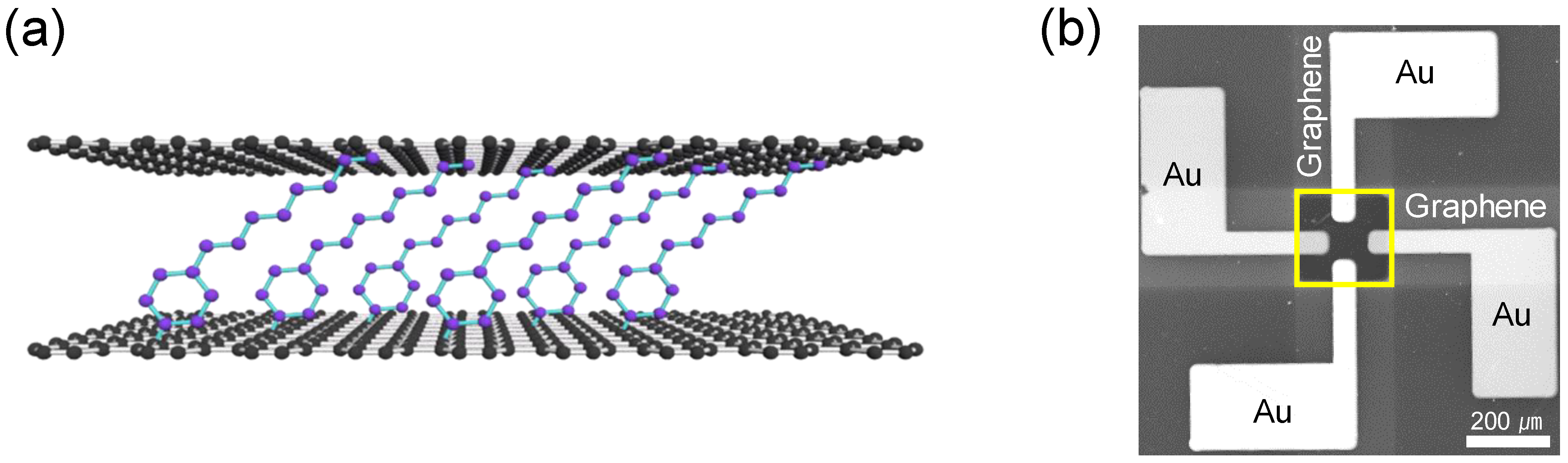
2. Experimental Details

The schematic of a device structure is seen in Figure 1a, which was based on arylalkane monolayers anchored between two (top and bottom) graphene electrodes. To fabricate the device, a pre-patterned Au(100 nm)/Ti(3 nm) bottom contact pad was first deposited on oxidized Si wafers using an electron-beam evaporator at the low evaporation rate of ~0.1 Å/s. A single layer graphene (from Graphene Square), grown on a Cu foil by chemical vapor deposition, was transferred as a bottom electrode on the oxidized Si substrate. We employed a well-known poly(methyl methacrylate) (PMMA)-mediated graphene transfer method [25], in which a thermal-release tape was applied to the PMMA film spin-coated on the bottom graphene. The Cu foils were eliminated in the solution of 20 g/L ammonium persulfate in distilled water for more than 10 h, and the release tapes and PMMA were removed by warm acetone after the graphene transfer. Afterward, the bottom graphene was patterned through a shadow mask by O2 plasma treatment. For molecular deposition, 20~50 mM diazonium compounds of arylalkanes were dissolved within dimethylformamide (DMF). The graphene-transferred substrates were submersed in the diazonium solution for a minimum of 24 h. Arylalkanes for three different lengths, denoted in the following as ArC8, ArC10, and ArC12 by the number of a C atom in the alkyl chain, were anchored to the bottom graphene via a dediazonization reaction [26]. This process allowed for a robust covalent bond between the bottom graphene and aryl diazonium compounds. The arylalkanes on the bottom graphene were rinsed with DMF to remove residual molecules and then dried completely in a vacuum chamber. The top graphene and Au (100 nm) contact pad were deposited on the molecular layers, the same as the procedures to create the bottom electrodes. As a final step, the redundant graphene and molecules out of the junction area were eliminated by O2 plasma to avoid parasitic conducting paths. Figure 1b shows a top-view image of scanning electron microscopy (SEM) for the whole device fabricated, where the junction area, highlighted in a yellow square box, ranged from 4.0 × 10 8 to 6.3 × 10 8   m 2 (200–250 μm on a side). We used a Raman spectroscopy (NOST, FEX, Seongnam-si, Korea) and atomic force microscopy (AFM) (Park Systems, XE7, Suwon-si, Korea) to inspect the pristine and monolayer-covered graphenes and a Keithley 4200A-SCS parameter analyzer (Keithley Instruments, Solon, OH, USA) and Janis cryostat for transport measurements.

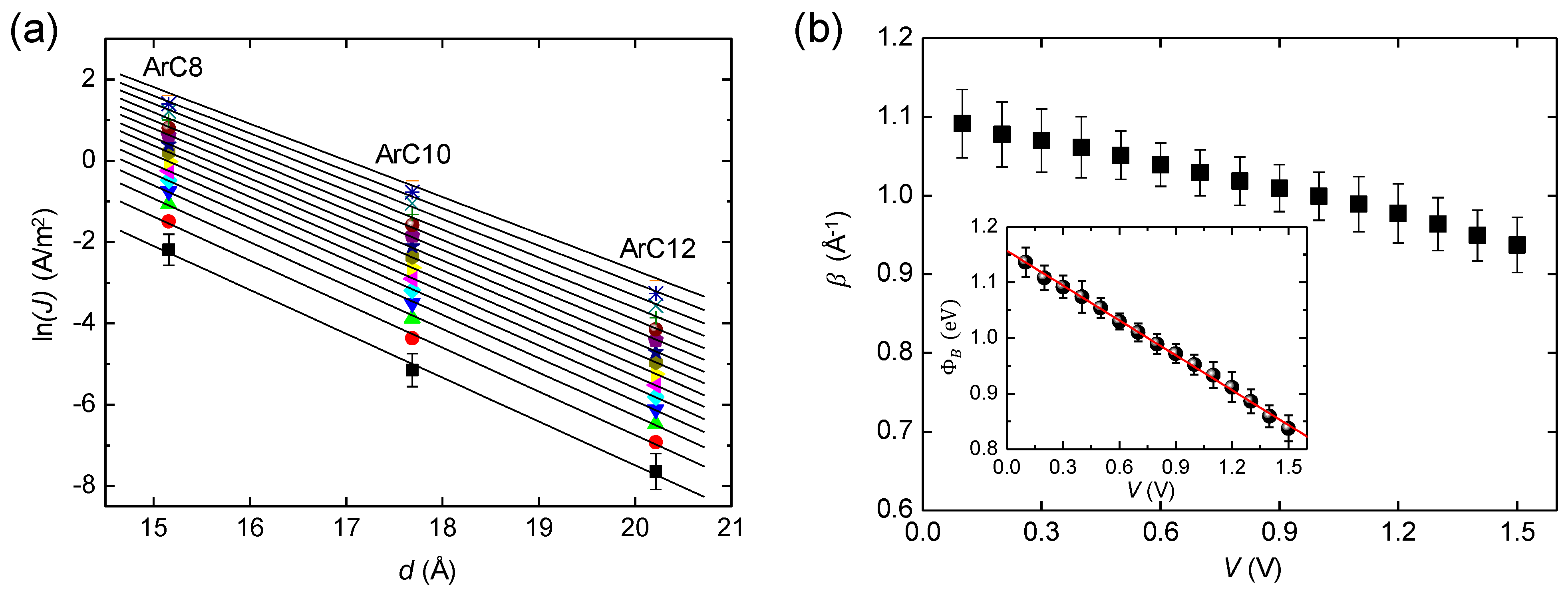
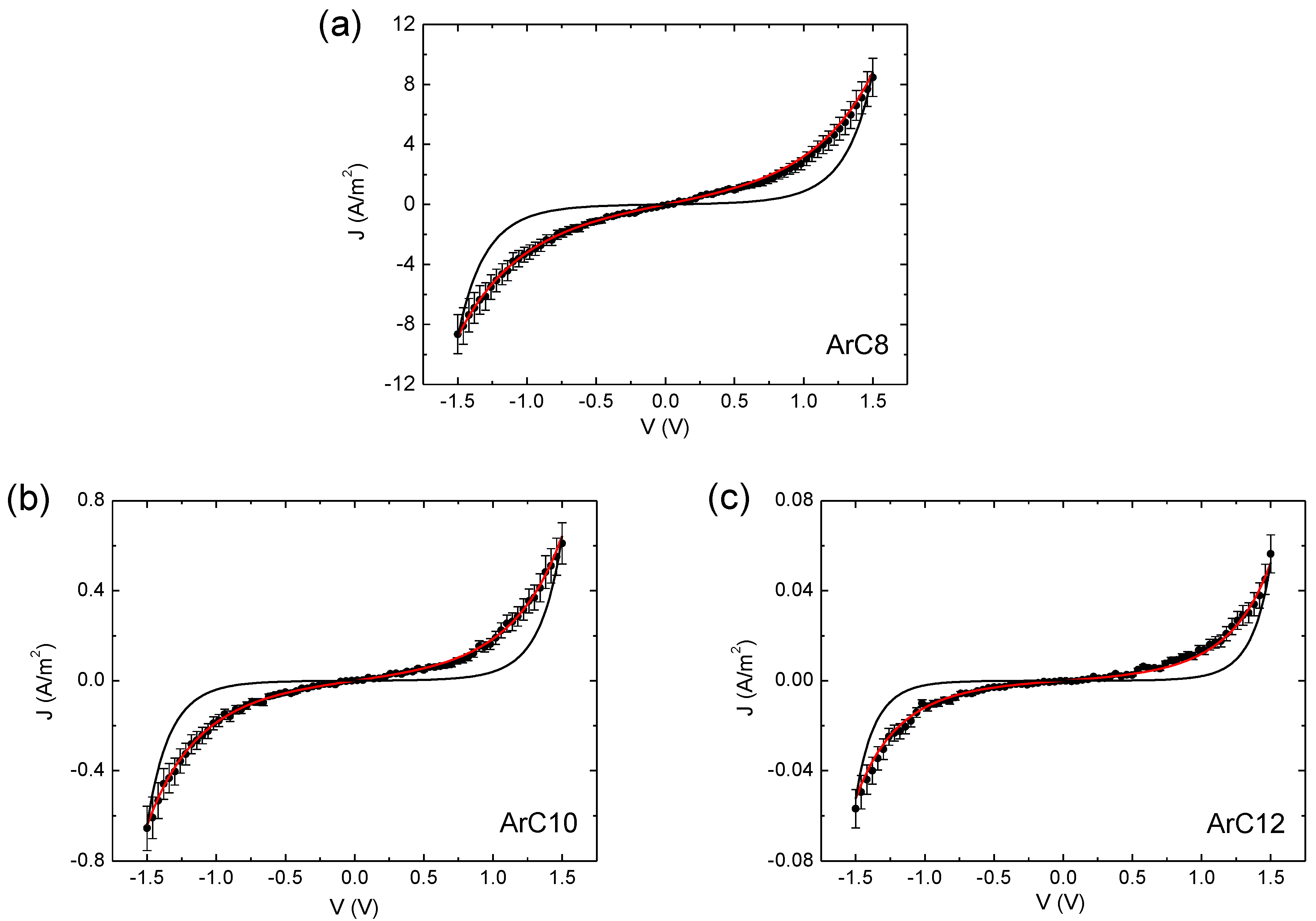
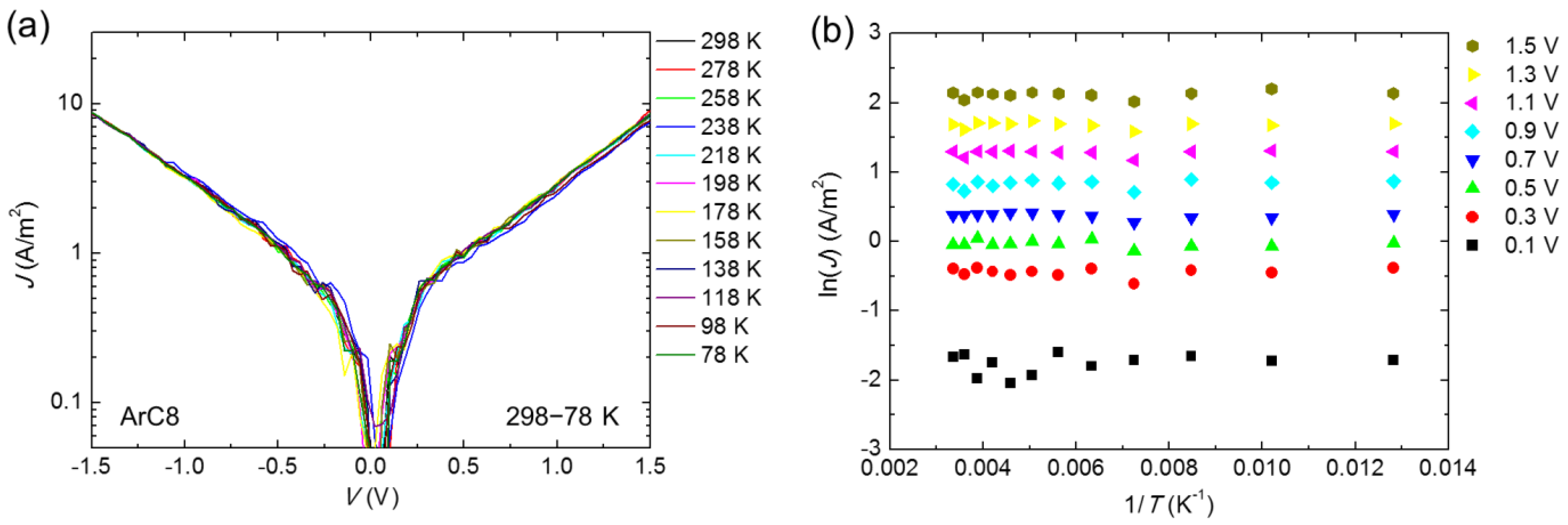
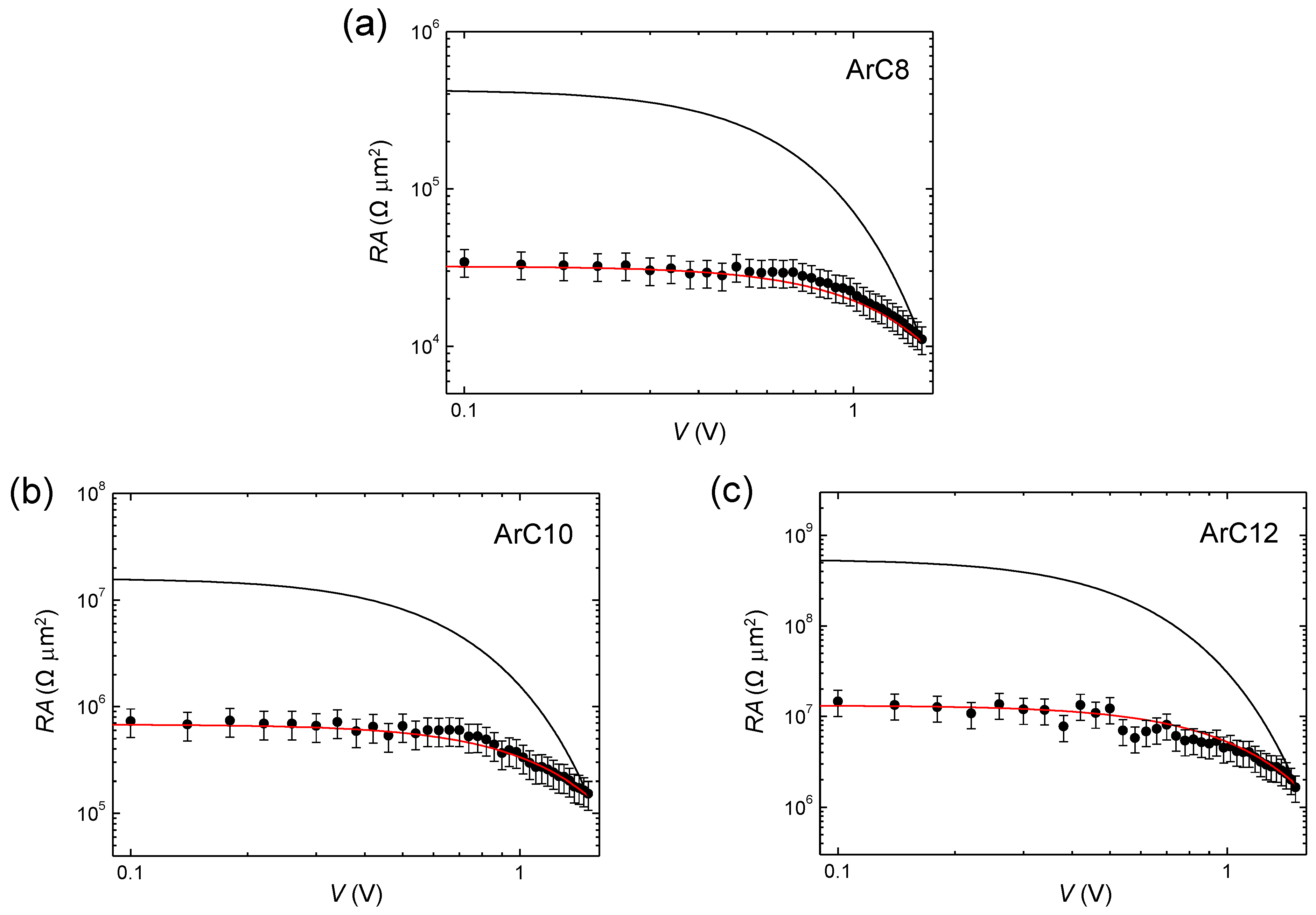
3. Results and Discussion

The fabrication of a molecular junction based on SAMs mostly involves the deposition of the metal atoms for a top-side contact on a few nanometer-thick molecular layers. This process frequently results in a short circuit failure due to direct penetration of the evaporated metal atoms through SAMs, thus destroying the molecular junctions. To prevent this problem, here we employed the graphene film as a protecting interlayer for the stable formation of a molecule–electrode top contact. We also note that the graphene contacts did not take part in the molecular tunnel junctions as actively tunable components with the gate modulation [27,28], which was beyond the scope of the present study.
We measured the Raman spectra of the pristine and arylalkane (ArC10)-covered graphenes transferred on the substrates (see Figure S1). Two typical prominent peaks of the G band (1581 cm−1) and 2D band (2674 cm−1) and a large ratio (>~2.3) of Raman intensity between the G and 2D bands indicated that the transferred graphene film was a single layer [29]. The absence of the D peak (1349 cm−1) in the pristine graphene implied that it was of good quality without substantial defects. The Raman peak corresponding to the D band appeared after the attachment of the arylalkane molecules to the graphene, which can be caused by the defects, resulting from the formation of a covalent C−C sp3 bond between the molecules and graphene [26,29]. From the line profile analysis of the AFM images (see Figure S2), the height of the ArC10-grafted and pristine graphenes’ layers transferred to the SiO2 surface was measured as 2.5 and 0.5 nm, respectively. The offset of ~2 nm was nearly comparable to the molecular length. In total, the results for the Raman spectroscopy and AFM measurements consistently indicated the SAM formation onto the bottom graphene.
As the Fermi level (EF) of electrodes is located within a large HOMO–LUMO gap of the short-length arylalkane series, tunneling via the molecular barrier can be rationally anticipated as the dominant transport mechanism of these junctions [22,23]. However, in the absence of variable-temperature characterization, other thermally activated mechanisms such as hopping conduction or thermionic emission cannot be ruled out. Figure 2a shows the representative semilogarithmic JV characteristic of an ArC8 junction measured from the device structure described in Figure 1. It was obtained in a sufficiently wide temperature variation (from 298 to 78 K) and with 20 K steps to verify the conduction mechanism. The current density barely changed, which was in agreement with the results measured with similar metal/alkyl molecules/metal junctions. Figure 2b displays an Arrhenius analysis of the current density. The slope of ln(J) against 1/T at different biases exhibited no significant dependence, thus manifesting the absence of thermal activation. The measurements on ArC10 and ArC12 showed also little temperature dependence (see Figure S3). Hence, we concluded that charge tunneling is maintained as the conduction mechanism through arylalkane monolayers incorporated between graphene electrodes. Now that we established tunneling as the transport mechanism, theoretical calculations from a tunneling model could be used to simulate our molecular junctions based on a graphene heterostructure.
One of the most essential parameters related to tunneling through a molecular junction is the decay coefficient ( β ), which can be determined by performing the length-dependent transport measurements based on the Simmons model [11,22,24]. Figure 3a shows ln(J) values plotted against the molecular length of arylalkanes at the different biases. By using ACD/Lab software, the molecular lengths of ArC8, ArC10, and ArC12 were estimated to be 13.3, 18.2, and 23.2 Å, respectively. The tunneling current densities were calculated from the average of approximately 80 devices per each molecule, indicating exponential dependency upon the molecular length ( d ) for a given bias. This length dependence represented a general feature of non-resonant tunneling, described by J   exp ( β d ) [8,13,23]. The decay coefficient at each bias was determined from the slopes of linear fits and is displayed in Figure 3b. The uncertainty of the β values in Figure 3b denotes a linear fit error. The decay coefficients ranged from 1.08 to 0.92 Å−1, dependent on the applied voltages. These values were similar to that of alkyl-based junctions with metallic contacts [13,24]. Our analysis of this length-dependent transport showed that the arylalkane monolayer not only maintained its molecular integrity in the junction but also predominated the charge transport properties and was not disturbed by the graphene–molecule contacts. Overall, temperature-independent and exponentially length-dependent JV characteristics consistently showed the non-resonant tunneling transport for these junctions. These findings ruled out defect-mediated transport in the molecular tunnel barrier and graphene contacts, which is typically expected to show thermally activated transport characteristics [10,13].
Within the Simmons model of a rectangular barrier (i.e., α = 1 ), the relationship between the tunneling decay coefficient and barrier height ( Φ B ) is given by [21,27]:
β = 2 2 m Φ B
where m is the bare electron mass and h   ( = 2 π ) is the Planck constant. Using Equation (1), the Simmons barrier heights calculated from the β values at different biases are plotted in the inset of Figure 3b, where the barrier height linearly depends on the magnitude of the bias voltage. Our findings indicated that the increasing bias voltage led to lower tunneling barrier, thus decreasing the decay coefficient. This effect may be attributed to image potential, which has been known to reduce the barrier height and, therefore, enhances the probability of charge tunneling across molecular barriers [18,19]. The extraction of β and Φ B was then straightforward by performing the length-dependent transport characterization, without adjustable fitting parameters. Based on the linear relation (red, solid line) observed in the inset of Figure 3b, the voltage dependence of the barrier height could be approximated as
Φ B ( V ) = γ | e V | + Φ B 0
where Φ B ( V ) and Φ B 0 are defined as the bias-voltage dependent and zero-bias barrier height, respectively, in units of eV, and γ signifies the degree of the voltage dependency on the barrier height as a unitless constant. In this linear relationship, γ and Φ B 0 can be determined from the slope and y-intercept, respectively, by which γ = 0.21 ± 0.01 and Φ B 0 = 1.16 ± 0.01 eV are found in the inset of Figure 3b. The voltage dependence of a barrier height was also previously reported for porphyrin molecular junctions formed by a conducting AFM technique without the length-dependent measurements [30].
The statistically representative J–V curves (data points) are presented in Figure 4 and were obtained by averaging all the data measured at 78 K for each arylalkane molecule with different lengths. The error bars indicate a 1σ standard error of the mean value. The traces of the J–V curves are almost symmetric in respect to the origin and display a nonlinearity that was shown to be more prominent as increasing the bias We initially tested the original Simmons model (see Equation (S1)) based on a constant rectangular barrier to simulate the representative J–V curves [18], where the barrier height was used as a fitting parameter. Apparently, there was inconsistency between the constant barrier approximation and the experimental J–V curves. As seen in Figure 4, the fitted current density (black, solid curves) with the constant barrier increased abruptly near ±1.1 V from an almost flat value, whereas the experimental J–V data rose gradually in a sigmoidal shape. This fitting result showed that the Simmons model based on the constant barrier height was not suitable to characterize the J–V curves of the graphene tunnel junctions without a further adjustable parameter.
Therefore, we presented an alternative method, where the Simmons model was modified with a voltage-induced barrier lowering (VIBL), quantitatively characterized by the length-dependent transport measurements. The significance of VIBL is that it allows for our experimental J–V curves to be simulated over a full bias range of | V | 1.5   V by incorporating Equation (2) as the VIBL parameter in the Simmons model. Then, the modified Simmons equation expresses the current density through a molecular tunnel barrier as:
J = e 4 π 2 d 2 { ( Φ B ( V ) e V 2 ) exp ( 2 d 2 m Φ B ( V ) e V 2 ) ( Φ B ( V ) + e V 2 ) exp ( 2 d 2 m Φ B ( V ) + e V 2 ) }
Figure 4 demonstrates that the representative JV characteristics averaged from extensive measurements on the tunnel junctions can be described with the modified Simmons simulation (red, solid curves) using Equation (3), where VIBL is included as Φ B ( V ) in the model. As described above, the VIBL parameter Φ B ( V ) was experimentally determined by the length-dependent analysis using Equations (1) and (2). It is noted that the JV curves were not “fitted” and, thus, there was no need for the adjustable fitting parameters. The simulation with Φ B ( V ) was accurate within the errors of measurements over the entire bias range, offering a better description for the measured JV curves, as compared to the conventional constant barrier approximation. A clear consensus between the experimental and simulated transport characteristics demonstrated the validity for the use of the Simmons model combined with VIBL for the case of our graphene-based molecular junctions.
A critical verification of the VIBL approximation is if this model can exactly predict the experimental results. For a self-consistency check, we replotted the experimental and simulated data, as displayed in Figure 5, where the resistance R multiplied by the junction area A is shown on a logarithmic scale against the bias voltage for each molecule investigated [19]. Simmons earlier presented this analysis in the original paper to examine the effect of fitting parameters on the tunneling model [18]. We note that the log plot of RA versus V was beneficial to especially reveal the further details concerning the validity of the tunneling model. The simulations plotted using the VIBL model (red lines) precisely described the measurements (data points) in the whole bias region, as likewise observed in Figure 4. The fitting results with the constant barrier model are also plotted in Figure 5 (black lines), where the disagreement between the experiment and model is much more profound and the fits clearly seem to be not accurate over the entire voltage regime. With the barrier height alone as a fitting parameter, the analysis of RA versus V indicated that it was not possible to characterize the molecular tunnel junctions based on graphene electrodes.

4. Conclusions

The charge transport through vertical graphene/arylalkane/graphene heterojunctions was investigated by the Simmons model combined with the bias-voltage dependence of a tunneling barrier height. Both the temperature independence and exponential length dependence of the measured JV characteristics clearly showed that non-resonant tunneling is the dominant conduction mechanism in these junctions. The tunneling decay coefficients at different bias voltages were determined by inspecting an exponential decrease in the current density with the molecular length, for an arylalkane series contacted between top and bottom graphene electrodes. The decay coefficient ranged from 1.08 to 0.92 Å−1 depending on the bias voltage. Based on the Simmons model, the length-dependent transport analysis indicated γ = 0.21 ± 0.01 and Φ B 0 = 1.16 ± 0.01 eV for the arylalkane tunnel junctions. The critical parameter Φ B ( V ) of VIBL was experimentally extracted from the bias dependence of β . Then, we employed the Simmons model modified with Φ B ( V ) to simulate the charge transport characteristics measured from graphene-based molecular junctions. Irrespective of the molecular length, the representative JV data were in agreement with the simulation without adjustable fitting parameters over the whole range of applied voltage ( | V | 1.5   V ), which was consistently revealed by the analysis of RA versus V plots on a logarithmic scale. The high quality of the simulations justifies the use of the VIBL-modified Simmons model for analysis of graphene-based molecular junctions. As presented in this study, the graphene contacts in molecular junctions effectively protect the molecular SAMs from penetration by the evaporated metal atoms, providing a stable test bed for the transport measurement. In addition, the incorporation of a gate electrode may become a fascinating future work to modulate the tunneling transport through graphene-based molecular devices.

Supplementary Materials

The following supporting information can be downloaded at: https://www.mdpi.com/article/10.3390/cryst12060767/s1, Figure S1: Raman spectrum for a pristine and ArC10-coverd graphene; Figure S2: AFM topographical images and line profile analyses of a pristine and ArC10-coverd graphene; Figure S3: Arrhenius plots of ArC10 and ArC12 junctions; Table S1: Comparison of various non-evaporative top contact molecular junctions [10].

Author Contributions

Conceptualization, H.S.; formal analysis, K.I. and D.-H.S.; investigation, K.I. and D.-H.S.; methodology, K.I.; supervision, H.S.; writing—original draft, H.S.; writing—review and editing, K.I., D.-H.S. and H.S. All authors have read and agreed to the published version of the manuscript.

Funding

This work was supported by the National Research Foundation of Korea (grant No. 2020R1F1A1076107).

Institutional Review Board Statement

Not applicable.

Informed Consent Statement

Not applicable.

Data Availability Statement

Data is contained within the article or supplementary material.

Conflicts of Interest

The authors declare no conflict of interest.

References

  1. Chen, H.; Stoddart, J.F. From molecular to supramolecular electronics. Nat. Rev. Mater. 2018, 6, 804–828. [Google Scholar] [CrossRef]
  2. Bryce, M.R. A review of functional linear carbon chains (oligoynes, polyynes, cumulenes) and their applications as molecular wires in molecular electronics and optoelectronics. J. Mater. Chem. C 2021, 9, 10524–10546. [Google Scholar] [CrossRef]
  3. Gupta, R.; Jash, P.; Sachan, P.; Bayat, A.; Singh, V.; Mondal, P.C. Electrochemical Potential-Driven High-Throughput Molecular Electronic and Spintronic Devices: From Molecules to Applications. Angew. Chem. Int. Ed. 2021, 60, 26904–26921. [Google Scholar] [CrossRef]
  4. Xin, N.; Guan, J.; Zhou, C.; Chen, X.; Gu, C.; Li, Y.; Ratner, M.A.; Nitzan, A.; Stoddart, J.F.; Guo, X. Concepts in the design and engineering of single-molecule electronic devices. Nat. Rev. Phys. 2019, 1, 211–230. [Google Scholar] [CrossRef]
  5. Fu, H.; Zhu, X.; Li, P.; Li, M.; Yang, L.; Jia, C.; Guo, X. Recent progress in single-molecule transistors: Their designs, mechanisms and applications. J. Mater. Chem. C 2022, 10, 2375–2389. [Google Scholar] [CrossRef]
  6. Caneva, S.; Gehring, P.; García-Suárez, V.M.; García-Fuente, A.; Stefani, D.; Olavarria-Contreras, I.J.; Ferrer, J.; Dekker, C.; Van Der Zant, H.S.J. Mechanically controlled quantum interference in graphene break junctions. Nat. Nanotechnol. 2018, 13, 1126–1131. [Google Scholar] [CrossRef]
  7. Zhang, J.L.; Zhong, J.Q.; Lin, J.D.; Hu, W.P.; Wu, K.; Xu, G.Q.; Wee, A.T.S.; Chen, W. Towards single molecule switches. Chem. Soc. Rev. 2015, 44, 2998–3022. [Google Scholar] [CrossRef] [PubMed] [Green Version]
  8. Gorenskaia, E.; Turner, K.L.; Martín, S.; Cea, P.; Low, P.J. Fabrication of metallic and non-metallic top electrodes for large-area molecular junctions. Nanoscale 2021, 13, 9055–9074. [Google Scholar] [CrossRef] [PubMed]
  9. Martín-Barreiro, A.; Soto, R.; Chiodini, S.; García-Serrano, A.; Martín, S.; Herrer, L.; Pérez-Murano, F.; Low, P.J.; Serrano, J.L.; Marcos, S.; et al. Uncapped Gold Nanoparticles for the Metallization of Organic Monolayers. Adv. Mater. Interfaces 2021, 8, 2100876. [Google Scholar] [CrossRef]
  10. Puebla-Hellmann, G.; Venkatesan, K.; Mayor, M.; Lörtscher, E. Metallic nanoparticle contacts for high-yield, ambient-stable molecular-monolayer devices. Nature 2018, 559, 232–235. [Google Scholar] [CrossRef]
  11. Akkerman, H.B.; Blom, P.W.M.; de Leeuw, D.M.; de Boer, B. Towards molecular electronics with large-area molecular junctions. Nature 2006, 441, 69–72. [Google Scholar] [CrossRef] [PubMed] [Green Version]
  12. Loo, Y.-L.; Lang, D.V.; Rogers, A.J.A.; Hsu, J.W.P. Electrical Contacts to Molecular Layers by Nanotransfer Printing. Nano Lett. 2003, 3, 913–917. [Google Scholar] [CrossRef]
  13. Jeong, H.; Kim, D.; Kwon, H.; Hwang, W.-T.; Jang, Y.; Min, M.; Char, K.; Xiang, D.; Jeong, H.; Lee, T. Statistical investigation of the length-dependent deviations in the electrical characteristics of molecular electronic junctions fabricated using the direct metal transfer method. J. Phys. Condens. Matter 2016, 28, 94003. [Google Scholar] [CrossRef] [PubMed]
  14. Neuhausen, A.B.; Hosseini, A.; Sulpizio, J.A.; Chidsey, C.E.D.; Goldhaber-Gordon, D. Molecular Junctions of Self-Assembled Monolayers with Conducting Polymer Contacts. ACS Nano 2012, 6, 9920–9931. [Google Scholar] [CrossRef]
  15. Wang, G.; Kim, Y.; Choe, M.; Kim, T.-W.; Lee, T. A New Approach for Molecular Electronic Junctions with a Multilayer Graphene Electrode. Adv. Mater. 2011, 23, 755–760. [Google Scholar] [CrossRef]
  16. Seo, S.; Min, M.; Lee, S.M.; Lee, H. Photo-switchable molecular monolayer anchored between highly transparent and flexible graphene electrodes. Nat. Commun. 2013, 4, 1920. [Google Scholar] [CrossRef] [Green Version]
  17. Kühnel, M.; Overgaard, M.H.; Hels, M.C.; Cui, A.; Vosch, T.; Nygård, J.; Li, T.; Laursen, B.W.; Nørgaard, K. High-Quality Reduced Graphene Oxide Electrodes for Sub-Kelvin Studies of Molecular Monolayer Junctions. J. Phys. Chem. C 2018, 122, 25102–25109. [Google Scholar] [CrossRef]
  18. Simmons, J.G. Generalized Formula for the Electric Tunnel Effect between Similar Electrodes Separated by a Thin Insulating Film. J. Appl. Phys. 1963, 34, 1793–1803. [Google Scholar] [CrossRef] [Green Version]
  19. Akkerman, H.B.; Naber, R.C.G.; Jongbloed, B.; van Hal, P.A.; Blom, P.W.M.; de Leeuw, D.M.; de Boer, B. Electron tunneling through alkanedithiol self-assembled monolayers in large-area molecular junctions. Proc. Natl. Acad. Sci. USA 2007, 104, 11161–11166. [Google Scholar] [CrossRef] [Green Version]
  20. Huisman, E.H.; Guédon, C.M.; van Wees, B.J.; van der Molen, S.J. Interpretation of Transition Voltage Spectroscopy. Nano Lett. 2009, 9, 3909–3913. [Google Scholar] [CrossRef] [Green Version]
  21. Xie, Z.; Bâldea, I.; Smith, C.E.; Wu, Y.; Frisbie, C.D. Experimental and Theoretical Analysis of Nanotransport in Oligophenylene Dithiol Junctions as a Function of Molecular Length and Contact Work Function. ACS Nano 2015, 9, 8022–8036. [Google Scholar] [CrossRef]
  22. Wang, W.; Lee, T.; Reed, M.A. Mechanism of electron conduction in self-assembled alkanethiol monolayer devices. Phys. Rev. B 2003, 68, 035416. [Google Scholar] [CrossRef]
  23. Holmlin, R.E.; Haag, R.; Chabinyc, M.L.; Ismagilov, R.F.; Cohen, A.E.; Terfort, A.; Rampi, M.A.; Whitesides, G.M. Electron Transport through Thin Organic Films in Metal−Insulator−Metal Junctions Based on Self-Assembled Monolayers. J. Am. Chem. Soc. 2001, 123, 5075–5085. [Google Scholar] [CrossRef] [PubMed] [Green Version]
  24. Engelkes, V.B.; Beebe, A.J.M.; Frisbie, C.D. Length-Dependent Transport in Molecular Junctions Based on SAMs of Alkanethiols and Alkanedithiols: Effect of Metal Work Function and Applied Bias on Tunneling Efficiency and Contact Resistance. J. Am. Chem. Soc. 2004, 126, 14287–14296. [Google Scholar] [CrossRef]
  25. Liang, X.; Sperling, B.A.; Calizo, I.; Cheng, G.; Hacker, C.; Zhang, Q.; Obeng, Y.; Yan, K.; Peng, H.; Li, Q.; et al. Toward Clean and Crackless Transfer of Graphene. ACS Nano 2011, 5, 9144–9153. [Google Scholar] [CrossRef] [PubMed]
  26. MacLeod, J.M.; Rosei, F. Molecular Self-Assembly on Graphene. Small 2014, 10, 1038–1049. [Google Scholar] [CrossRef] [PubMed]
  27. Kumar, S.B.; Seol, G.; Guo, J. Modeling of a vertical tunneling graphene heterojunction field-effect transistor. Appl. Phys. Lett. 2012, 101, 033503. [Google Scholar] [CrossRef] [Green Version]
  28. Fallahazad, B.; Lee, K.; Kang, S.; Xue, J.; Larentis, S.; Corbet, C.; Kim, K.; Movva, H.C.P.; Taniguchi, T.; Watanabe, K.; et al. Gate-Tunable Resonant Tunneling in Double Bilayer Graphene Heterostructures. Nano Lett. 2015, 15, 428–433. [Google Scholar] [CrossRef]
  29. Zhu, Y.; Murali, S.; Cai, W.; Li, X.; Suk, J.W.; Potts, J.R.; Ruoff, R.S. Graphene and Graphene Oxide: Synthesis, Properties, and Applications. Adv. Mater. 2010, 22, 3906–3924. [Google Scholar] [CrossRef]
  30. Nawarat, P.; Beach, K.; Meunier, V.; Terrones, H.; Wang, G.-C.; Lewis, K.M. Voltage-Dependent Barrier Height of Electron Transport through Iron Porphyrin Molecular Junctions. J. Phys. Chem. C 2021, 125, 7350–7357. [Google Scholar] [CrossRef]
Figure 1. (a) Schematic of graphene/arylalkane/graphene heterojunctions. The arylalkane (ArC8) monolayer is sandwiched between top and bottom graphene contacts. (b) An SEM image of the fabricated device. The active area of a molecular junction is highlighted by a yellow square box.
Crystals 12 00767 g001
Figure 2. (a) Variable-temperature JV characteristics with temperature variation from 298 to 78 K with 20 K steps, displayed in different color lines. (b) Arrhenius plot of ArC8 junctions at voltages from 0.1 to 1.5 V with 0.2 V steps.
Crystals 12 00767 g002
Figure 3. (a) Plot of ln(J) versus d for the bias range from 0.1 (bottom) to 1.5 V (top). For clarity, the data only at 0.1 V contain the error bar, indicating the standard deviation upon averaging the current density. The β values were determined from the slope of the linear fits (solid line). (b) Plot of β versus V. The inset shows the bias-voltage dependence of the barrier height. The solid line indicates the linear fit.
Crystals 12 00767 g003
Figure 4. The statistically representative J–V curves (data points), obtained by averaging all the data measured at 78 K for (a) ArC8, (b) ArC10, and (c) ArC12 junctions. Black curves indicate the fitting results of the original Simmons model with a constant barrier height, and red curves denote the simulation of the VIBL-modified Simmons model.
Crystals 12 00767 g004
Figure 5. Log plots of RA versus V for (a) ArC8, (b) ArC10, and (c) ArC12 junctions. The fits with the original Simmons model for a constant barrier height (black curves) and the simulation of the VIBL-modified Simmons model (red curves) are shown.
Crystals 12 00767 g005
Publisher’s Note: MDPI stays neutral with regard to jurisdictional claims in published maps and institutional affiliations.

