Article

Improved Optoelectronic Characteristics of Ga-In co-Doped ZnO UV Photodetectors by Asymmetric Metal Contact Structure

Department of Materials Science and Engineering, Feng Chia University, Taichung 40724, Taiwan
*
Author to whom correspondence should be addressed.
Crystals 2022, 12(5), 746; https://doi.org/10.3390/cryst12050746
Submission received: 10 April 2022 / Revised: 14 May 2022 / Accepted: 16 May 2022 / Published: 23 May 2022
(This article belongs to the Special Issue Optoelectronics and Photonics in Crystals)

Abstract

:
Transparent Ga and In co-doped ZnO (ZnO:Ga-In) semiconductor thin films were deposited on Corning glass substrates by the sol-gel spin-coating process. The ZnO:Ga-In thin films were used as the sensing layer of metal–semiconductor–metal (MSM)-type ultraviolet (UV) photodetectors (PDs). In this study, the optoelectronic characteristics of ZnO:Ga-In MSM PDs with symmetrical interdigital electrodes (Al–Al) and asymmetrical interdigital electrodes (Al–Au) were compared. The as-prepared ZnO:Ga-In thin films were polycrystalline, and they had a single-phase hexagonal wurtzite structure and high transparency (~88.4%) in the visible region. The MSM-PDs with asymmetric electrodes had significantly reduced dark current (9.6 × 10⁻⁵ A at 5 V) according to the current-voltage (I-V) characteristics and higher photoresponse properties than those of the MSM-PDs with symmetric electrodes, according to the current-time (I-t) characteristics. In addition, the Al–Au devices were self-powered without an applied bias voltage. The photocurrent was 6.0 × 10⁻⁵ A; the sensitivity and responsivity were 0.25 and 0.03 mA/W, respectively, under UV illumination.

1. Introduction

Transparent functional oxide thin films such as ZnO-based multicomponent materials have been studied intensively, and they have been considered for application in advanced displays, smart sensors, and portable and wearable electronic devices [1,2,3]. It is already well-known that extrinsic dopants (for example, elements in groups II, III, and IV) can be incorporated into ZnO thin films to modify their physical properties [4,5]. Previous investigations have demonstrated that co-doping with two types of extrinsic dopants is an efficient approach to considerably improve the electrical characteristics and optical parameters of ZnO-based thin films [6,7]. The ionic radii of Ga3+ (0.62 Å) and In3+ (0.81 Å) are slightly different from that of Zn2+ (0.74 Å), but these ions can be substituted for Zn2+ in the ZnO host sites without causing excessive lattice distortion [8]. Simultaneously co-doping Ga and In ions reduces the lattice strain (stress) due to compensation for the introduced tensile and compressive stresses in the ZnO lattice [7]. The two extrinsic dopants have the same valence electron configuration and can co-exist in n-type ZnO semiconductor materials as dual donors to increase the free carrier concentration.
Li et al. have reported that ZnO co-doping with In and Ga allows the fabrication of high-reliability optoelectronic functional materials [9]. Vorobyeva et al. have reported that the incorporation of both In and Ga into spin-coated ZnO thin films improves the average transmittance in the visible region and significantly increases the conductivity to 3.6 S/cm, which is three orders higher than that of the undoped ZnO thin film [10]. Kang et al. developed 2 mol% In and Ga co-doped ZnO sol-gel thin films treated with sequential RTA and laser annealing processes, which exhibited the lowest sheet resistance of 15.9 kΩ/sq [11].
Ultraviolet (UV) photodetectors (PDs), which can convert optical signals into an electrical current, are prominent optoelectronic devices that are widely used in scientific, industrial, military, and space exploration applications [12,13]. The key issue in the preparation of PDs that have high photoelectric performance and save energy, and electricity is the efficient separation of photogenerated electron–hole pairs [14]. Various approaches have been developed to establish a built-in electronic field in the absorbing layer of photodetectors so as to make them self-powered, i.e., able to operate at zero voltage bias [15]. Two such approaches are p-n junction diodes [16] and metal–semiconductor–metal structure devices with asymmetric metal electrodes [17,18].
The geometry of metal–semiconductor–metal photodetectors (MSM-PDs) includes back-to-back metal–semiconductor (MS) contacts [18]. Due to their simple structure, MSM-PDs can simplify the fabrication process and improve the manufacturing yield. They have attracted the interest of scientists because, despite their large bandwidth, their photoresponse speed is limited by the intrinsic RC constant [19]. In addition, the dark current of MSM-PDs is greater than that of other photodiode detectors. Casalino et al. reported that the dark current of MSM-PDs can be suppressed with the use of different metal electrodes and/or by depositing different electrode contact areas [19]. If two different work function metals (one being a low work function metal, such as Al and In, and the other being a high work function metal, such as Au and Ni) are chosen as asymmetrical interdigital electrodes for MSM-PDs and can provide a built-in potential gradient to improve the current conduction, the photoresponse properties may allow the photoelectric sensor to be self-powered [18].
The sol-gel and spin-coating process is a typical chemical solution deposition process for the preparation of large-area functional oxide films. It has several attractive features, including low-cost equipment, a simple process, easy adjustment of the chemical composition, flexible integration with microelectronics processes, and high efficiency in technological production [20,21]. The influence of asymmetric metal contacts on the photoresponse of GaN MSM-PDs has been reported. However, the improvement of the photosensing characteristics of solution-processed ZnO-based MSM-PDs by an asymmetric contact structure has not been studied. In this study, the authors prepared ZnO:Ga-In transparent semiconductor thin films, which exhibited the qualities of optoelectronic devices, for application as the sensing layer of MSM-PDs. The photodetection properties of ZnO:Ga-In MSM-PDs with Al-Al symmetric electrodes and Al–Au asymmetric electrodes were compared. In addition, the work function difference between the Al and Au metals allowed us to fabricate an Al/ZnO:Ga-In/Au UV photodetector with an asymmetric metal contact structure, which could lead to UV light detection without an externally applied voltage to achieve a self-powered MSM-PD.

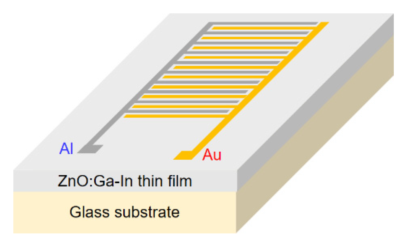
2. Materials and Methods

An analytical reagent grade solvent, stabilizer, and metallic salts were used in the present study to ensure experimental repeatability and reproducibility. Zinc acetate dihydrate (Zn(CH3CO2)2·2H2O, J.T. Baker, CAS No. 5970-45-6), gallium(III) nitrate hydrate (Ga(NO3)·xH2O, Alfa Aesar, CAS No. 69365-72-6), and indium(III) nitrate hydrate (In(NO3)·xH2O, Alfa Aesar, CAS No. 207389-97-8) were selected as the raw materials of Zn, Ga, and In ions, respectively. 2-methoxyethanol (2-ME, Acros Organics, CAS No. 109-86-4) and monoethanolamine (MEA, Acros Organics, CAS No. 141-43-5) were used as the solvent and stabilizer. Extrinsic dopants of Ga and In were added in the same stoichiometric amounts, and the total sum of the doping level was at 2 at% in the resultant solution. The concentration of metal ions in the resultant solution was 0.4 M, and the molar ratio of MEA stabilizer to metal ions was kept at 1. The coating precursor was synthesized by dissolving stoichiometric amounts of metallic salts (1.728 g zinc acetate + 0.0204 g gallium nitrate + 0.0240 g indium nitrate) in solvent (20 ml) and stabilizer (0.4877 mL) at 60 °C for 2 h to yield a clear and transparent solution. Corning EAGLE XG glass substrates (5 cm × 5 cm × 0.7 mm, Corning Inc., Corning, NY, USA) were cleaned sequentially using acetone and alcohol with ultrasonic vibration before being dried on a hot plate prior to the deposition of the metal oxide sol-gel films.
The Ga-In co-doped ZnO (ZnO:Ga-In) sol-gel films were spin-coated onto the pre-cleaned glass substrates. The first 3 ml of the as-synthesized sol was dropped onto a glass substrate at a rotation of 1000 rpm for 30 s. Each as-coated sol-gel film was dried at 300 °C for 10 min to evaporate the solvent and burn off organic compounds. After spin-coating and drying procedures were performed twice, the dried sol-gel films were annealed in a quartz tube furnace under ambient air at 500 °C for 1.5 h to remove residual organic matter and achieve crystalline oxide films. With a pair of designed fine metal shadow masks, asymmetric metal electrodes of Al and Au were deposited and patterned onto the ZnO:Ga-In thin film by the thermal evaporation method in a two-step deposition process. The device size, interdigital electrode width, and spacing of the metal–semiconductor–metal photodetectors (MSM-PDs) were 8.85 mm × 4.15 mm, 150 μm, and 150 μm, respectively. As exhibited in Figure 1, Al–Au symmetrical interdigital electrodes were deposited onto the ZnO:Ga-In semiconductor layer to fabricate the MSM structured photodetectors.
The crystal structure of the as-prepared ZnO:Ga-In thin films was examined by X-ray diffraction (XRD, Bruker D8 Discover). The surface morphology studies were performed with a scanning probe microscope (SPM, Digital Instruments NS4/D3100CL/MultiMode), and the microstructures were investigated in cross-section with a field-emission scanning electron microscope (FE-SEM, Hitachi S-4800). The chemical composition and core-level binding energy were examined by X-ray photoelectron spectroscopy (XPS, ULVAC-PHI PHI 5000 VersaProbe). An ultraviolet-visible (UV-Vis) spectrophotometer (Hitachi U-2900) was utilized to record the light transmission spectrum; a Hall measurement system (Ecopia HMS-3000) was employed to measure the room-temperature electrical properties. The current–voltage (I-V) relationships and photoresponse performance measurements were carried out with a Source-Measure Unit (Jiehan 5600) in darkness and in UVA light illumination conditions. The transient photoresponses of the MSM-PDs were measured with mercury lamps as the light source; these lamps provided an incident power density of 2.2 mW/cm2.

3. Results and Discussion

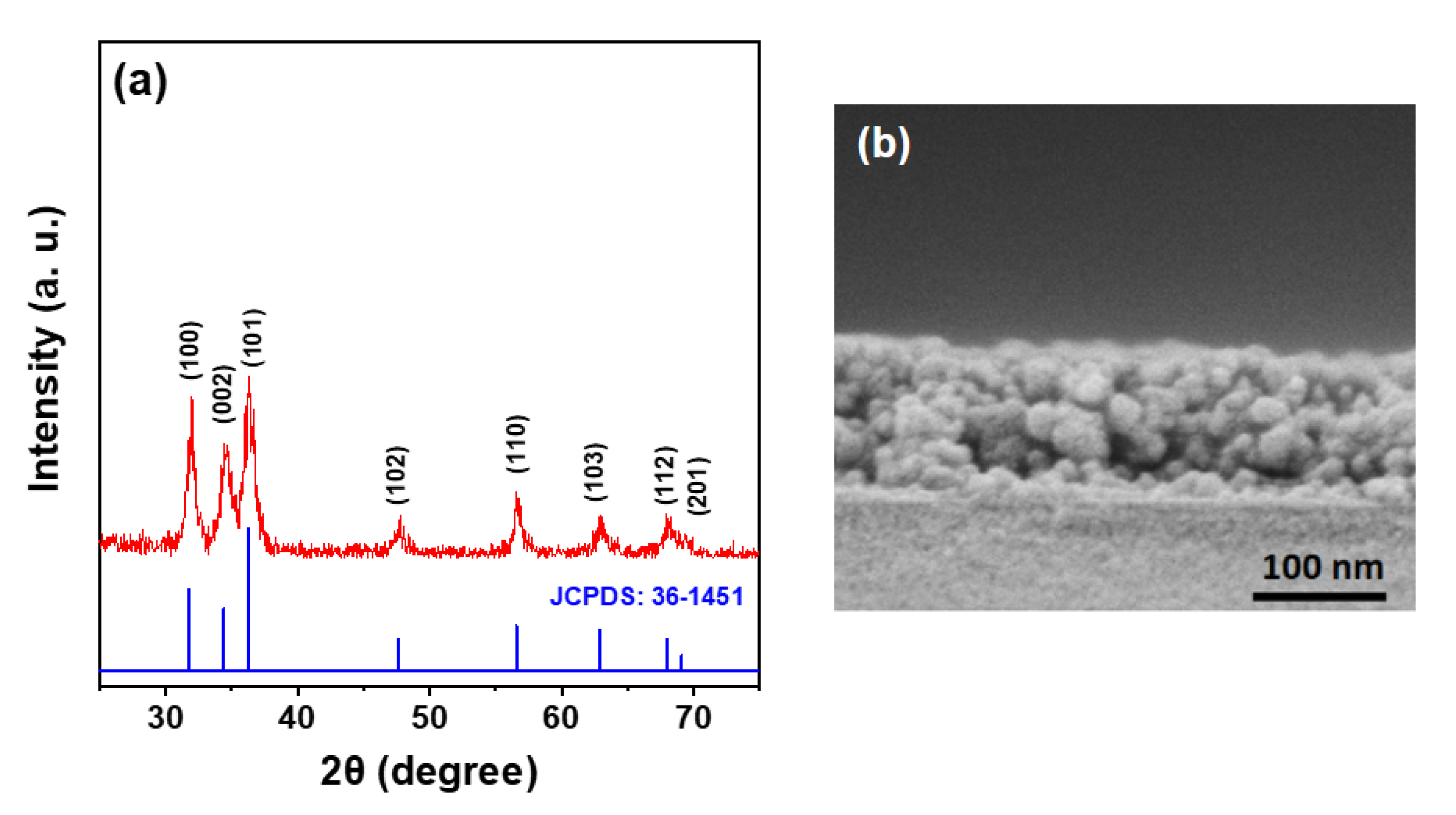
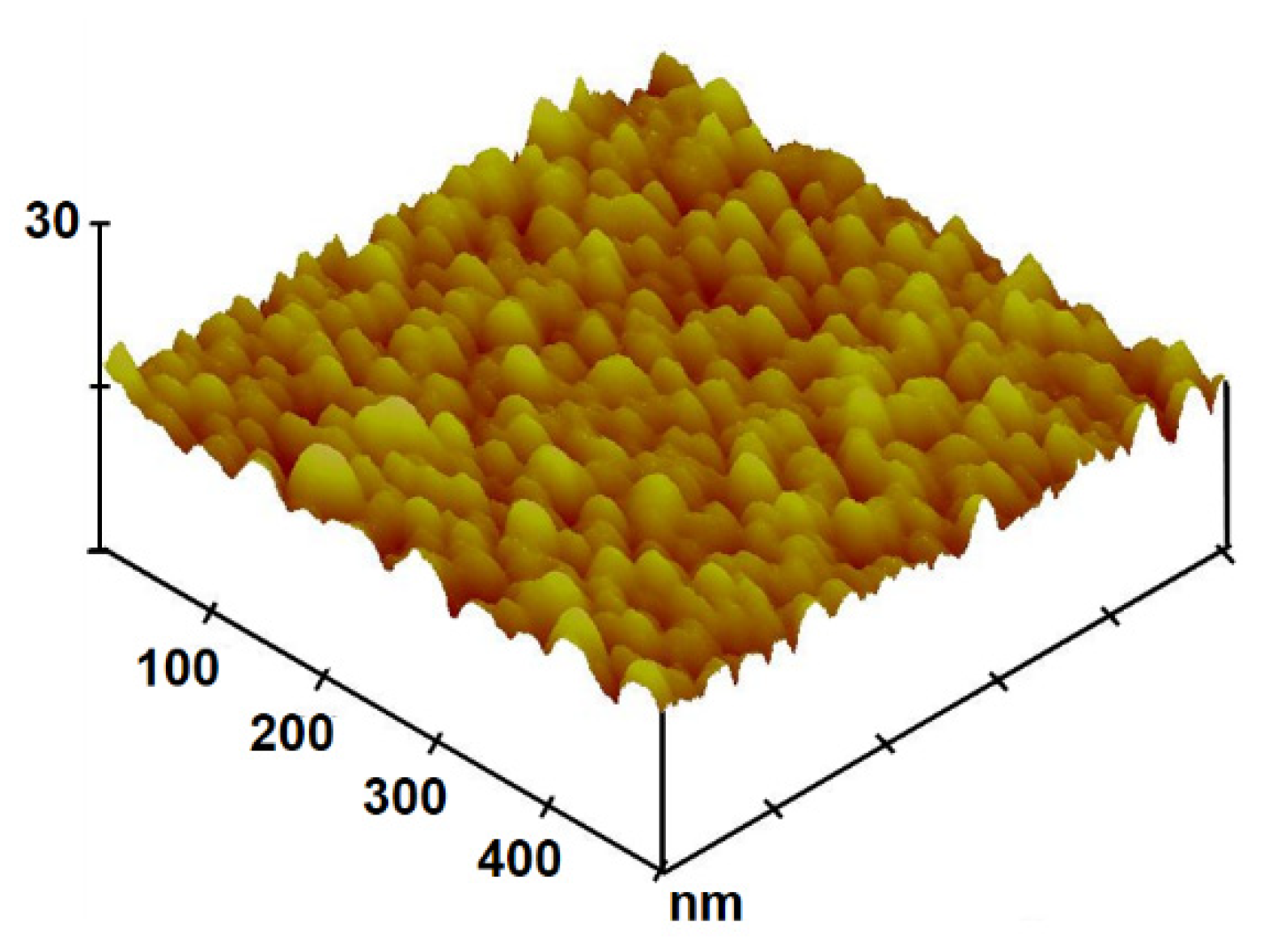
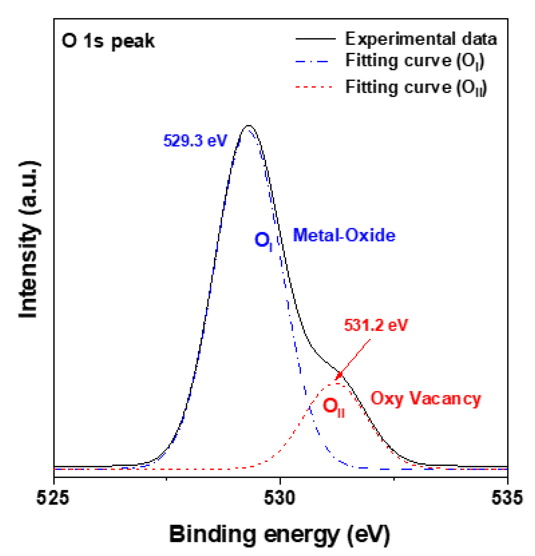
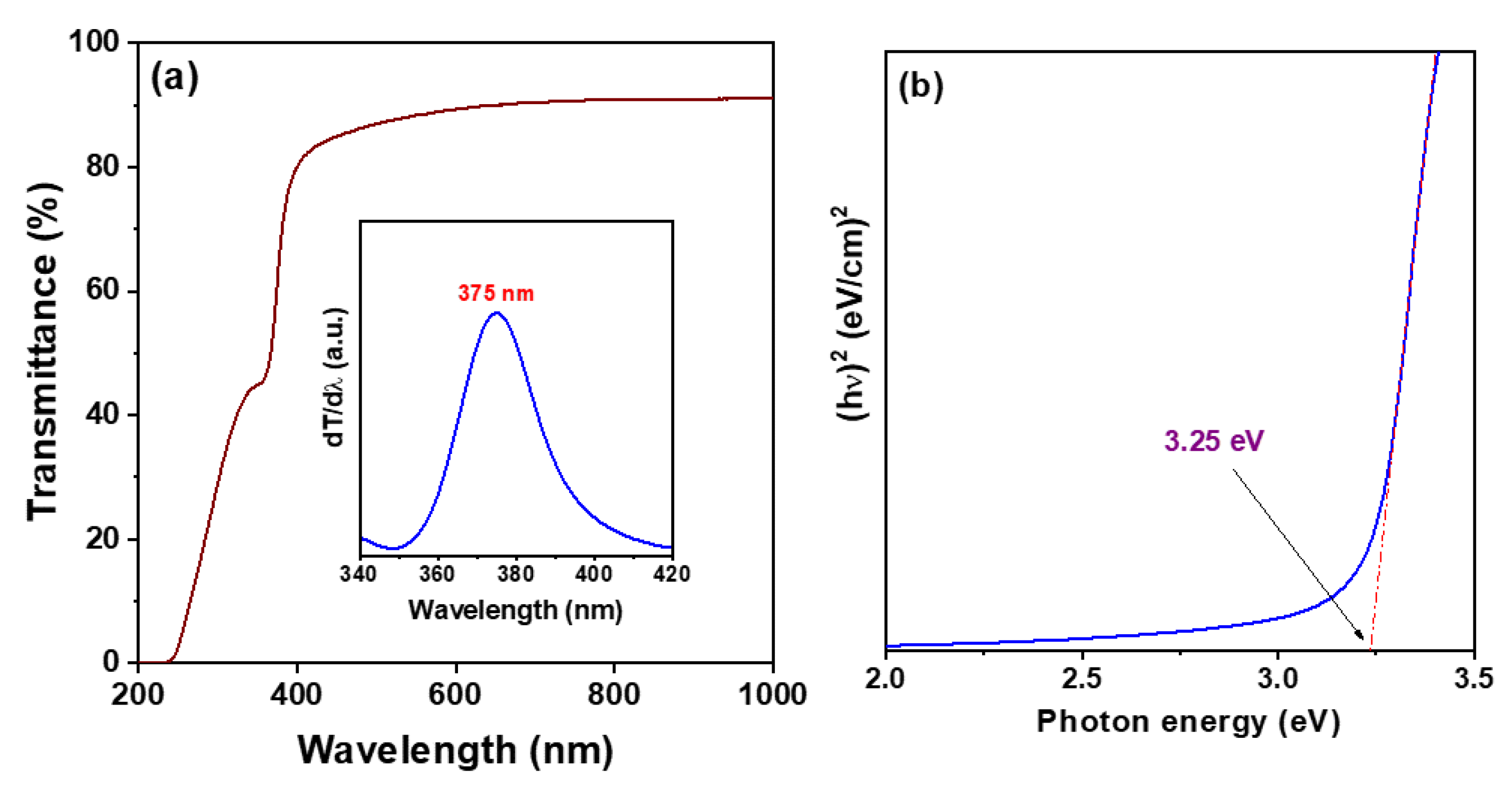
3.1. Characteristics of Sol-Gel Derived ZnO:Ga-In Thin Films

The phase structure of the as-prepared oxide thin films was examined by XRD. Figure 2a shows the XRD pattern of annealed Ga-In co-doped ZnO (ZnO:Ga-In) sol-gel film. Eight observable diffraction peaks indicated that the as-prepared oxide thin film had the typical polycrystalline structure, corresponding to the (100), (002), (101), (102), (110), (103), (112), and (201) crystallographic planes of JCPDS card number 36-1451 for wurtzite ZnO crystals. These results confirmed the formation of the hexagonal wurtzite phase. In addition, no other diffraction signals were detected in the XRD pattern, implying the successful preparation of single-phase ZnO-based thin film. The average crystallite size of the obtained ZnO-based thin film was estimated by Scherrer’s formula [22] from the three main diffraction peaks of the (100), (002), and (101) planes from the XRD data. The calculated average crystallite size was 8.63 nm, which was smaller than the report of Vorobyeva et al. (15 nm), who prepared (Ga, In) co-doped ZnO thin films by spin-coating and annealing at 500 °C for 6 h [10].
An FE-SEM micrograph presenting a cross-sectional view of the sol-gel-derived ZnO-based thin film on the glass substrate is shown in Figure 2b. As can be seen in the SEM image, the inside of the obtained oxide film possessed obviously granular microstructures and a uniform thickness. It was also found that nano-sized pores were retained inside the ZnO-based thin film; these defects were ascribed to the burnout of the precursor solution, and decomposition of residual organic compounds in the sol-gel derived oxide thin film [23]. The mean thickness of the ZnO:Ga-In thin film was determined from the cross-sectional FE-SEM micrograph to be 132.5 nm.
The surface morphology and root-mean-square (RMS) roughness of the obtained ZnO:Ga-In thin film was investigated by SPM. A three-dimensional (3D) SPM image acquired from the free surface of a glass/oxide thin film sample is presented in Figure 3. The image shows a granular structure without microcracks or tiny pores; the surface consisted of close-packed nano-sized particles. The average particle size, estimated from the corresponding 3D SPM image, was 39.3 nm, and the surface RMS roughness of the ZnO-based thin film samples was 3.3 nm.
The presence of the expected elements (Ga, In, Zn, and O) in the obtained ZnO-based thin film was confirmed by a broad scan XPS analysis (data not shown). The narrow scan XPS examination identified the chemical bonding states of O in the thin film sample. Figure 4 shows the core level XPS spectrum of O 1s, which exhibited a broad, significantly asymmetric feature in the high binding energy region (solid line). The curve of the experimental data (high-resolution O 1s XPS spectrum) was deconvoluted by a Gaussian curve fitting into two distinct sub-curves (dashed lines), which denoted the areas of two components, with OI and OII for the corresponding two oxygen levels [24]. The component on the low binding energy (OI) side had strong intensity. It was centered at about 529.3 eV and attributed to O2− ions bonded with metal ions (Zn2+, Ga3+, or In3+), such as O-Zn bonds, in the hexagon wurtzite ZnO lattice. The component of the high binding energy (OII) side was centered at 531.2 eV. It was related to the O2 ions close to the oxygen-deficient regions and associated with the concentration of oxygen vacancies. Thus, a change in this component area would correspond to an alteration in the oxygen-vacancy concentration. The OII/Ototal area ratio for the ZnO:Ga-In thin film was 19.30%. The result revealed that the Ga-In co-doped ZnO thin films had a higher OII/Ototal area ratio than that of the undoped ZnO thin film in a previous report (17.74%.) [21], indicating that weaker oxygen–metal bonds formed in the impurity co-doped ZnO-based thin film. This led to the high-level oxygen vacancy concentration in the as-prepared ZnO:Ga-In thin film.
The optical transmittance spectrum of the glass/thin film sample was measured to investigate the optical properties, and the results, presented in Figure 5a, revealed significant absorption in the UV region and high transparency in the visible spectrum region. Due to the direct and wide bandgap of greater than 3.2 eV, the ZnO:Ga-In thin film sample exhibited good average visible light transmittance of 88.4% in the wavelength range of 400–800 nm. The first derivative of the optical transmittance (T) with optical wavelength (λ) was calculated to estimate the absorption edge position of the oxide thin film sample. The plot of dT/dλ versus wavelength is provided in the inset of Figure 5a; the position of the maximum peak corresponded to the optical band-edge absorption of the ZnO-based thin film. As shown in that plot, the peak position for ZnO:Ga-In thin film was 375 nm, which is close to that of the 2 at% Al-doped ZnO semiconductor thin film (372 nm) [21].
Optical transitions can occur as direct transitions between the valence band maximum (VBM) and conduction band minimum (CBM) for direct bandgap oxide semiconductors or compound semiconductors. Therefore, we evaluated the optical bandgap (Eg) with allowed direct transitions according to Tauc’s relation [25]:
(αhν)2 = B (hν − Eg),
where hν is the photon energy and the coefficient B is an energy-independent constant relevant to the band-tailing states. The plot of the variation of (αhν)2 with the photon energy (eV) (namely, the Tauc plot), which was acquired from the recorded transmittance data, is shown in Figure 5b. The optical bandgap (Eg) of the ZnO:Ga-In thin film was determined by extrapolating the linear portion near the onset of the absorption edge of the absorption curve with the photon energy (hv) on the X axis. The determined optical bandgap was 3.25 eV, which is close to the report of Potter et al. [6], who synthesized In and Ga co-doped ZnO thin film by chemical vapor deposition.
Hall effect measurements at room temperature revealed that the as-prepared ZnO:Ga-In thin films had an n-type nature and mean electrical resistivity (ρ) of 1.27 × 10² Ω·cm, with a mean electron concentration (n) of 8.88 × 1015 cm−3 and a mean Hall mobility (μ) of 5.54 cm2/Vs. These electrical characteristics are slightly better than those of the Al-B co-doped ZnO semiconductor thin film (ρ = 3.21 × 10² Ω·cm and n = 1.55 × 1015 cm−3) [21].

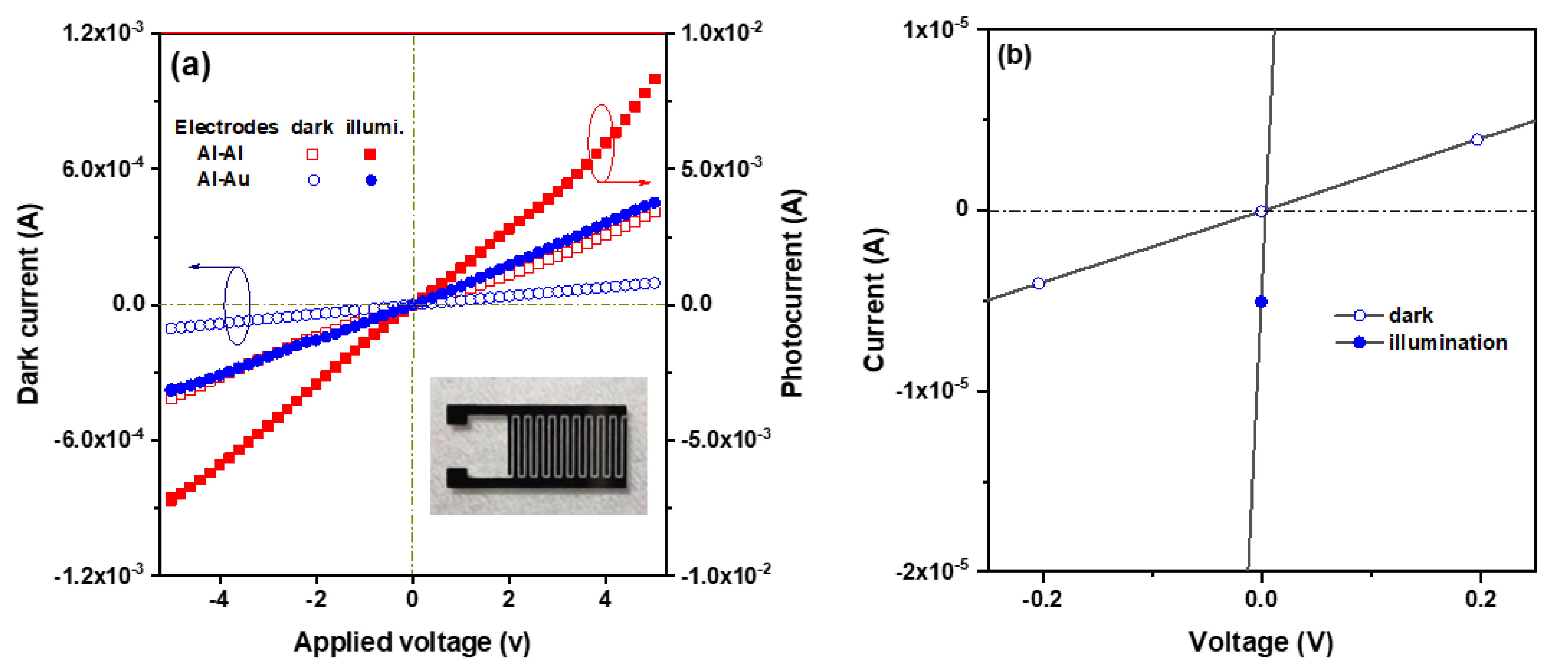
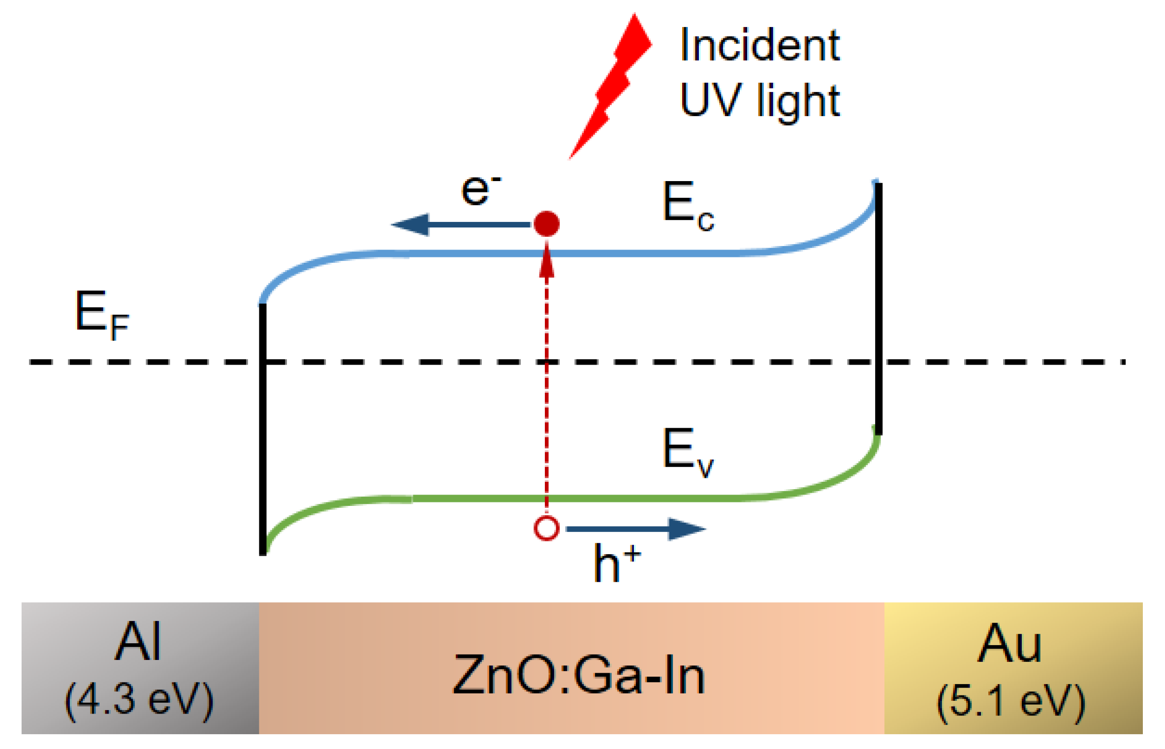
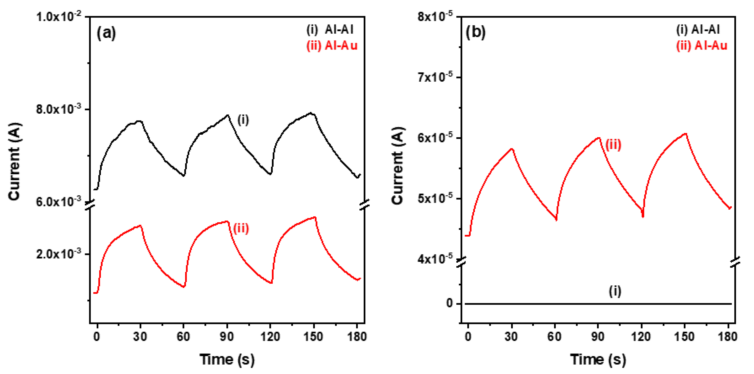
3.2. Performance of the ZnO:Ga-In UV Photodetectors

Figure 6a shows the current–voltage (I-V) characteristics of the two kinds of MSM-PDs (with symmetric or asymmetrical electrodes) in the dark condition and under UV light illumination. A voltage sweep from −5 V to +5 V was applied across the two interdigitated electrodes. The digital photograph of the as-fabricated ZnO:Ga-In MSM PD with asymmetrical Al–Au interdigital electrodes is shown in the inset of Figure 6a. Both the dark current and the photocurrent rose in direct proportion to the increases in applied voltage because the internal electrical field between the interdigital electrodes was proportional to the external voltage applied to the contact pads. It is noted that the asymmetric electrodes device exhibited a lower dark current level than that of the symmetric electrodes device; the resistances of the corresponding devices, determined by Ohm’s law (R = V/I), were 4.99 × 10⁴ Ω (Al–Au device) and 1.29 × 10⁴ Ω (Al–Al device) in the dark condition. In addition, the illumination-to-dark current ratios for the symmetrical electrodes and asymmetrical electrodes devices were 20.3 and 39.0, respectively. The I-V characteristics demonstrated that the application of a pair of asymmetric metal electrodes to ZnO-based semiconductor thin film can effectively lower the dark current and significantly improve the photosensing property. Moreover, Figure 6b shows that the asymmetric electrodes device exhibited a low level of photocurrent under UVA illumination at zero bias voltage (solid circle).
The contact barriers were established at the interfaces between the ZnO:Ga-In layer and the two metal electrodes (Al and Au). It is well-known that the nature of metal–semiconductor (MS) contacts is determined by the work function (Φm) of the metals and the conduction band (Ec) edge of the semiconductors. Energy band diagram of the two different work function metals, Al (Φm = 4.3 eV) and Au (Φm = 5.3 eV), were used as asymmetric contacts for the n-type ZnO:Ga-In semiconductor layer, as shown in Figure 7.
Figure 8a presents the time-dependent photoresponses of ZnO-based MSM photodetectors under illumination by UVA light with an intensity of 2.2 mW/cm2 at 5 V bias voltage. The two kinds of devices exhibited similar increases and decreases in photocurrent. These changes were dependent on the period of the turn-on and turn-off of the UVA light, indicating good repeatability and stability of those photodetectors. The rise and decay times for Al–Al and Al–Au devices were computed to be 20.4 s and 15.5 s, and 22.4 s and 21.2 s, respectively. The photodetection mechanism of the polycrystalline metal oxide semiconductors was quite different from the elemental and compound semiconductors. It is generally agreed that the absorption and adsorption of molecular oxygen (O2) on the surfaces of nanostructured oxide semiconductors play important roles in the photoresponse process. Xu et al. proposed that these relatively long rise and decay times can be attributed to the adsorption/desorption of oxygen molecules on the surfaces of nanostructured ZnO thin films [26]. Figure 8b shows the photoresponse characteristics of the devices based on symmetric and asymmetric electrodes without an externally applied voltage (0 V bias). It is noted that there was no response from the MSM-PD with symmetric electrodes (curve (i) in Figure 8b), whereas the device with asymmetric electrodes exhibited a typical multiple response feature (curve (ii) in Figure 8b). Measured results of the latter demonstrated that the charge carriers were driven by force from the built-in electric field, which was created via the asymmetric metal contacts. Therefore, the photoelectric sensor was self-powered [14].
Several key photoresponse parameters are commonly utilized for evaluating the photoelectric performance of semiconductor photodetectors, including sensitivity (Sph), responsivity (Rph), external quantum efficiency (EQE), and detectivity (D*). They are defined by the following equations [15,27]:
Sph = Ion − Ioff/Ioff,
Rph = Ion − Ioff/PA,
EQE = Rphhc/eλ,
D* = Rph/(2eIoff/S)1/2,
where Ion is the photocurrent under illumination, Ioff is the current detected in the dark condition, P is the power density of the incident light, A is the effective illumination area, h is Planck’s constant, c is the speed of light, e is the electron charge, and λ is the incident light wavelength. The sensitivity is related to the signal-to-noise level upon exposure to incident light. The responsivity indicates the photoelectric conversion efficiency of the photoelectronic device. EQE reveals the photocarrier generation efficiency in the device by the incident light, and the detectivity is associated with the ability to detect a weak signal of photodetector for studying noise-related signals [28,29].
The values of sensitivity for the devices with symmetric and asymmetric electrodes were 0.19 and 0.97, respectively, at 5 V bias under UVA light illumination. The corresponding responsivity, external quantum efficiency, and detectivity for determining the performance of the photodetectors are listed in Table 1. It was found that the asymmetric electrodes device exhibited better photoresponse characteristics than those of the symmetric electrodes device at 5 V bias voltage. At the same time, we also found that the asymmetric electrodes device was able to operate without an externally applied voltage. Its sensitivity and responsivity were 0.25 and 0.03 mA/W, respectively. The relatively low responsivity may be ascribed to the photoresponse mechanisms of self-powdered MSM-PDs.
Table 2 lists previous results related to the performance of MSM UV photodetectors with solution-processed impurity-doped and undoped nanostructured ZnO sensing layers [30,31,32,33,34]. The sensitivity of ZnO:Ga-In MSM-PDs with asymmetric electrodes (0.97) was higher than that of a ZnO nanorods doubly transparent UV sensor (0.213) [32] but lower than that of MSM-PDs with impurity-doped ZnO thin films (>25) [33,34]. In addition, it is noted that the magnitude of detectivity of the ZnO-based nanorods MSM-PDs was much higher than that of the developed ZnO:Ga-In MSM-PDs [30,31]. This feature can be attributed to the large surface area to volume ratio of oxide nanorods.

4. Conclusions

ZnO:Ga-In transparent semiconductor thin films and MSM UV photodetectors (PDs) with Al–Al symmetric and Al–Au asymmetric interdigitated electrodes have been successfully prepared on glass substrates by a sol-gel spin-coating process. The obtained single-phase polycrystalline ZnO:Ga-In semiconductor thin films had a wide optical bandgap of 3.25 eV and exhibited an n-type nature with moderate electrical properties. They had a mean electron concentration of 8.88 × 1015 cm−3, a mean Hall mobility of 5.54 cm2/V·s, and a mean electrical resistivity of 1.27 × 10² Ω·cm. Compared to conventional MSM-PDs with symmetric electrodes, the MSM-PDs with asymmetric electrodes had significantly improved photoresponse characteristics at 5 V bias, and they were also self-powered without applied voltage under UV illumination. The photocurrent was 6.0 × 10⁻⁵ A; the sensitivity and responsivity were 0.25 and 0.03 mA/W, respectively. This study presents the possibility of MSM-PDs with asymmetric metal contacts as an effective approach to achieving self-powered photoresponse characteristics.

Author Contributions

Conceptualization, C.-Y.T. and H.-M.T.; methodology, C.-Y.T., H.-M.T. and Y.-C.C.; validation, C.-Y.T.; investigation, C.-Y.T. and H.-M.T.; resources, C.-Y.T.; data curation, C.-Y.T., H.-M.T. and Y.-C.C.; writing—original draft preparation, C.-Y.T. and H.-M.T.; writing—review and editing, C.-Y.T.; project administration, C.-Y.T. All authors have read and agreed to the published version of the manuscript.

Funding

This work was funded by the Ministry of Science and Technology of Taiwan under Grant numbers MOST 108-2221-E-035-042.

Institutional Review Board Statement

Studies did not involve humans or animals.

Informed Consent Statement

The study did not involve humans.

Data Availability Statement

Data sharing is not applicable to this article.

Acknowledgments

The authors would like to thank the Precision Instrument Support Center of Feng Chia University for supporting XRD, FE-SEM, and SPM characterization facilities and the Instrument Center of National Chung Hsing University, Taichung, Taiwan, for assisting XPS measurement.

Conflicts of Interest

The authors declare no conflict of interest.

References

  1. Borysiewicz, M.A. ZnO as a functional material, a review. Crystals 2019, 9, 505. [Google Scholar] [CrossRef] [Green Version]
  2. Radzimska, A.K.; Jessionowski, T. Zinc oxide-from synthesis to application: A review. Materials 2014, 7, 2833–2881. [Google Scholar] [CrossRef] [PubMed] [Green Version]
  3. Özgür, Ü.; Hofstetter, D.; Morkoc, H. ZnO devices and applications: A review of current status and future prospects. Proc. IEEE 2010, 98, 1255–1268. [Google Scholar] [CrossRef]
  4. Shohany, B.G.; Zak, A.K. Doped ZnO nanostructures with selected elements-structural, morphology and optical properties: A review. Ceram. Int. 2020, 45, 5507–5520. [Google Scholar] [CrossRef]
  5. Tsay, C.Y.; Lee, W.C. Effect of dopants on the structural, optical and electrical properties of sol–gel derived ZnO semiconductor thin films. Curr. Appl. Phys. 2013, 13, 60–65. [Google Scholar] [CrossRef]
  6. Potter, D.B.; Powell, M.J.; Parkin, I.P.; Carmalt, C.J. Aluminium/gallium, indium/gallium, and aluminium/indium co-doped ZnO thin films deposited viaaerosol assisted CVD. J. Mater. Chem. C 2018, 6, 588–597. [Google Scholar] [CrossRef] [Green Version]
  7. Lim, J.H.; Lee, S.M.; Kim, H.S.; Kim, H.Y.; Park, J.; Jung, S.B.; Park, G.C.; Kim, J.; Joo, J. Synergistic effect of Indium and Gallium co-doping on growth behavior and physical properties of hydrothermally grown ZnO nanorods. Sci. Rep. 2017, 7, 41992. [Google Scholar] [CrossRef] [Green Version]
  8. Shaheera, M.; Girija, K.G.; Kaur, M.; Geetha, V.; Debnath, A.K.; Vatsa, R.K.; Muthe, K.P.; Gadkari, S.C. Elucidation of structural, morphological, optical and photoluminescence properties of single and (In, Ga) co-doped ZnO nanocrystalline thin films. Bull. Mater. Sci. 2019, 42, 266. [Google Scholar] [CrossRef] [Green Version]
  9. Li, H.; Schirra, L.K.; Shim, J.; Cheun, H.; Kippelen, B.; Monti, O.L.A.; Bredas, J.L. Zinc oxide as a model transparent conducting oxide: A Theoretical and Experimental Study of the Impact of Hydroxylation, Vacancies, Interstitials, and Extrinsic Doping on the Electronic Properties of the Polar ZnO (0002) Surface. Chem. Mat. 2012, 24, 3044–3055. [Google Scholar] [CrossRef]
  10. Vorobyeva, N.A.; Rumyantseva, M.N.; Vasiliev, R.B.; Kozlovskiy, V.F.; Soshnikova, Y.M.; Filatova, D.G.; Zaytsev, V.B.; Zaytseva, A.V.; Gaskov, A.M. Doping effects on electrical and optical properties of spin-coated ZnO thin films. Vacuum 2015, 114, 198–204. [Google Scholar] [CrossRef]
  11. Kang, J.; Jo, G.; Ji, J.H.; Koh, J.H. Improved electrical properties of laser annealed In and Ga co-doped ZnO thin films for transparent conducting oxide applications. Ceram. Int. 2019, 45, 23934–23940. [Google Scholar] [CrossRef]
  12. Sang, L.; Liao, M.; Sumiya, M. A comprehensive review of semiconductor ultraviolet photodetectors: From thin film to one-dimensional nanostructures. Sensors 2013, 13, 10482–10518. [Google Scholar] [CrossRef] [PubMed]
  13. Alaie, Z.; Nejad, S.M.; Yousefi, M.H. Recent advances in ultraviolet photodetectors. Mater. Sci. Semicond. Process. 2015, 29, 16–55. [Google Scholar] [CrossRef]
  14. Tao, J.; Xiao, Z.; Wang, J.; Li, C.; Sun, X.; Li, F.; Zou, X.; Liao, G.; Zou, Z. A self-powered, flexible photodetector based on perovskite nanowires with Ni-Al electrodes. J. Alloys Compd. 2020, 845, 155311. [Google Scholar] [CrossRef]
  15. Boruah, B.D. Zinc oxide ultraviolet photodetectors: Rapid progress from conventional to self-powered photodetectors. Nanoscale Adv. 2019, 1, 2059–2085. [Google Scholar] [CrossRef] [Green Version]
  16. Tsay, C.Y.; Hsiao, I.P.; Chang, F.Y.; Hsu, C.L. Improving the photoelectrical characteristics of self-powered p-GaN film/n-ZnO nanowires heterojunction ultraviolet photodetectors through gallium and indium co-doping. Mater. Sci. Semicond. Process. 2021, 121, 105295. [Google Scholar] [CrossRef]
  17. Chen, H.Y.; Liu, K.W.; Chen, X.; Zhang, Z.Z.; Fan, M.M.; Jiang, M.M.; Xie, X.H.; Zhao, H.F.; Shen, D.Z. Realization of a self-powered ZnO MSM UV photodetector with high responsivity using an asymmetric pair of Au electrodes. J. Mater. Chem. C 2014, 2, 9689–9694. [Google Scholar] [CrossRef]
  18. An, Y.; Liao, J.; Wu, C.; Zhang, R.; Li, Y.; Li, T. GaN MSM UV detectors with different electrode materials. J. Electron Devices Soc. 2021, 9, 1210–1214. [Google Scholar] [CrossRef]
  19. Casalino, M.; Iodice, M.; Sirleto, L.; Rendinam, I.; Coppola, G. Asymmetric MSM sub-bandgap all-silicon photodetector with low dark current. Opt. Express 2013, 21, 28072. [Google Scholar] [CrossRef]
  20. Ghodsi, F.E.; Absalan, H. Comparative study of ZnO thin films prepared by different sol-gel route. Acta Phys. Pol. A 2010, 118, 659–664. [Google Scholar] [CrossRef]
  21. Tsay, C.Y.; Yu, S.H. Melioration of electrical and optical properties of Al and B co-doped ZnO transparent semiconductor thin films. Coatings 2021, 11, 1259. [Google Scholar] [CrossRef]
  22. Cullity, B.D.; Stock, S.R. Elements of X-ray Diffraction, 3rd ed.; Prentice Hall: New Jersey, NY, USA, 2001; p. 170. ISBN 0-201-61091-4. [Google Scholar]
  23. Kim, Y.S.; Tai, W.P. Electrical and optical properties of Al-doped ZnO thin films by sol-gel process. Appl. Surf. Sci. 2007, 253, 4911–4916. [Google Scholar] [CrossRef]
  24. Park, G.C.; Hwang, S.M.; Lee, S.M.; Choi, J.H.; Song, K.M.; Kim, H.Y.; Kim, H.S.; Eum, S.J.; Jung, S.B.; Lim, J.H.; et al. Hydrothermally grown In-doped ZnO nanorods on p-GaN films for color-tunable heterojunction light-emitting-diodes. Sci. Rep. 2015, 5, 10410. [Google Scholar] [CrossRef] [PubMed] [Green Version]
  25. Tauc, J.; Scott, T.A. The optical properties of solids. Phys. Today 1967, 20, 105–107. [Google Scholar] [CrossRef]
  26. Xu, Q.; Cheng, L.X.; Meng, L.; Wang, Z.; Bai, S.; Tian, X.Q.; Jia, X.F.; Yong, Q. Flexible self-powered ZnO film UV sensor with a high response. ACS Appl. Mater. Interfaces 2019, 11, 26127–26133. [Google Scholar] [CrossRef]
  27. Jung, U.J.; Kim, S.B.; Kim, D.; Shin, D.S.; Xian, Z.; Park, J. Metal–semiconductor–metal UV detectors using transferrable amorphous and crystalline zinc-tin-oxide microsphere monolayers. ACS Sustain. Chem. Eng. 2020, 8, 60–70. [Google Scholar] [CrossRef]
  28. Ding, J.; Fang, H.; Lian, Z.; Li, J.; Lv, Q.; Wang, L.; Sun, J.L.; Yan, Q. A self-powered photodetector based on a CH3NH3PbI3 single crystal with asymmetric electrodes. CrystEngComm 2016, 18, 4405–4411. [Google Scholar] [CrossRef]
  29. Wu, C.Y.; Peng, W.; Fang, T.; Wang, B.; Xie, C.; Wang, L.; Yang, W.H.; Luo, L.B. Asymmetric contact-induced self-driven perovskite-microwire-array photodetectors. Adv. Electron. Mater. 2019, 5, 1900135. [Google Scholar] [CrossRef]
  30. Rana, A.u.H.S.; Shaikh, S.F.; Al-Enizi, A.M.; Agyeman, D.A.; Ghani, F.; Nah, I.W.; Shahid, A. Intrinsic control in defects density for improved ZnO nanorod-based UV sensor performance. Nanomaterials 2020, 10, 142. [Google Scholar] [CrossRef] [Green Version]
  31. Humayun, Q.; Kashif, M.; Hashim, U.; Qurashi, A. Selective growth of ZnO nanorods on microgap electrodes and their applications in UV sensors. Nanoscale Res. Lett. 2014, 9, 29. [Google Scholar] [CrossRef] [Green Version]
  32. Sarwar Rana, A.u.H.; Lee, J.Y.; Hong, Y.P.; Kim, H.S. Transient current response for ZnO nanorod-based doubly transparent UV sensor fabricated on flexible substrate. Phys. Status Solidi—Rapid Res. Lett. 2018, 12, 1800001. [Google Scholar] [CrossRef]
  33. Nurfani, E.; Kesuma, W.A.P.; Lailani, A.; Anrokhi, M.S.; Kadja, G.T.M.; Rozana, M.; Sipahutar, W.S.; Arif, M.F. Enhanced UV sensing of ZnO films by Cu doping. Opt. Mater. 2021, 114, 110973. [Google Scholar] [CrossRef]
  34. Tsay, C.Y.; Chen, S.T.; Fan, M.T. Solution-processed Mg-substituted ZnO thin films for metal-semiconductor-metal visible-blind photodetectors. Coatings 2019, 9, 277. [Google Scholar] [CrossRef] [Green Version]
Figure 1. Schematic illustration of the developed ZnO:Ga-In MSM UV photodetector with Al–Au asymmetrical interdigitated electrodes. A photodetector has 10 pairs of different work function metal electrodes.
Crystals 12 00746 g001
Figure 2. (a) X-ray diffraction (XRD) pattern of ZnO:Ga-In thin film deposited on glass substrate by sol-gel spin-coating and (b) cross-sectional FE-SEM micrograph of the corresponding sol-gel-derived ZnO:Ga-In thin-film sample.
Crystals 12 00746 g002
Figure 3. Three-dimensional (3D) scanning probe microscopy (SPM) micrograph of the surface of a ZnO:Ga-In thin film sample.
Crystals 12 00746 g003
Figure 4. The O 1s core-level XPS spectrum obtained from the ZnO:Ga-In thin film.
Crystals 12 00746 g004
Figure 5. (a) Optical transmission spectrum of glass/ZnO:Ga-In thin film sample. The inset shows the plot of dT/dλ versus wavelength of oxide film acquired from the optical transmittance data; (b) a Tauc plot for the corresponding ZnO:Ga-In thin film.
Crystals 12 00746 g005
Figure 6. (a) Comparison of current–voltage (I-V) characteristics for the ZnO:Ga-In MSM UV photodetectors with symmetric electrodes (Al and Al) or asymmetric electrodes (Al and Au) in the dark and UV illumination conditions. The inset shows a digital photograph of the Al–Au devices. (b) Magnified current–voltage (I-V) characteristics of the ZnO:Ga-In MSM-PD with Al–Au asymmetric electrodes in a bias voltage range from −0.2 V to 0.2 V.
Crystals 12 00746 g006
Figure 7. Schematic energy band diagram of the n-type ZnO:Ga-In semiconductor layer and Al–Au asymmetric electrodes without applied bias and under UV illumination.
Crystals 12 00746 g007
Figure 8. Time-resolved photocurrent curves measured under multiple on/off illumination cycles for photodetectors with symmetrical or asymmetrical interdigital contacts at bias voltage of (a) 5 V and (b) 0 V. The interval of UVA light illumination was maintained at 30 s.
Crystals 12 00746 g008
Table 1. Photoelectrical properties of ZnO:Ga-In MSM photodetectors with a pair of symmetrical or asymmetrical interdigitated electrodes under illumination of UV light.
DeviceBias Voltage (V)Sensitivity
(Iph/Ioff)
Responsivity
(mA/W)
External Quantum
Efficiency (%)
Detectivity   ( cm Hz / W )
Symmetric electrodes [Al–Al]50.193.251089.122.99 × 107
0------------
Asymmetric electrodes [Al–Au]50.973.381132.766.82 × 107
00.250.0310.053.25 × 105
Table 2. Comparison of results of different solution-processed ZnO-based MSM UV photodetectors.
Sensing MaterialElectrodes/
Substrate
Method/Temperature (°C)SensitivityResponsivity (mA/W)Illumin. WavelengthReference
ZnO:Ga nanorodsAg–Ag/glasshydrothermal/90---16,000368 nm[30]
ZnO nanorodsAu–Au/Sihydrothermal/90---2000300–370 nm[31]
ZnO nanorodsITO-ITO/PEThydrothermal/800.213---365 nm[32]
ZnO:Cu filmAg–Ag/glassspray/45025---365 nm[33]
Mg0.2Zn0.8O filmAu–Au/glasssol-gel/500281.18UVA[34]
ZnO:Ga-In filmAl–Au/glasssol-gel/5000.973.38UVAThis work
Publisher’s Note: MDPI stays neutral with regard to jurisdictional claims in published maps and institutional affiliations.

