Article

Hot-Pressed Two-Dimensional Amorphous Metals and Their Electronic Properties

1
Beijing National Laboratory for Condensed Matter Physics, Key Laboratory for Nanoscale Physics and Devices, Institute of Physics, Chinese Academy of Sciences, Beijing 100190, China
2
School of Physical Sciences, University of Chinese Academy of Sciences, Beijing 100190, China
3
Songshan Lake Materials Laboratory, Dongguan 523808, China
4
Beijing Key Laboratory for Nanomaterials and Nanodevices, Beijing 100190, China
*
Authors to whom correspondence should be addressed.
Crystals 2022, 12(5), 616; https://doi.org/10.3390/cryst12050616
Submission received: 14 March 2022 / Revised: 15 April 2022 / Accepted: 22 April 2022 / Published: 26 April 2022
(This article belongs to the Special Issue 2D Crystalline Nanomaterials)

Abstract

:
As an emerging research field, two-dimensional (2D) metals have been the subject of increasing research efforts in recent years due to their potential applications. However, unlike typical 2D layered materials, such as graphene, which can be exfoliated from their bulk parent compounds, it is hardly possible to produce 2D metals through exfoliation techniques due to the absence of Van der Waals gaps. Indeed, the lack of effective material preparation methods severely limits the development of this research field. Here, we report a PDMS-assisted hot-pressing method in glovebox to obtain ultraflat nanometer-thick 2D metals/metal oxide amorphous films of various low-melting-point metals and alloys, e.g., gallium (Ga), indium (In), tin (Sn), and Ga0.87Ag0.13 alloy. The valence states extracted from X-ray photoelectron spectroscopy (XPS) indicate that the ratios of oxidation to metal in our 2D films vary among metals. The temperature-dependent electronic measurements show that the transport behavior of 2D metal/metal oxide films conform with the 2D Mott’s variable range hopping (VRH) model. Our experiments provide a feasible and effective approach to obtain various 2D metals.

1. Introduction

Studies on 2D materials have advanced fundamental condensed matter physics and semiconductor engineering since the discovery of graphene [1]. Benefiting from the unique structural advantages of 2D layered materials, exotic physical phenomena have been studied in the extreme 2D limit [2]. In the aspect of electronic engineering applications, 2D metals/metal oxides have attracted great attention in recent years [3,4,5,6], showing great potential applications in catalysis [7], optoelectronics [8], sensors [9], and flexible electronics [10]. Considerable progress has been achieved in research on 2D metals and metal oxides. For example, Fang Yang et al. discovered topological edge states in single bismuth (Bi:111) bilayer [11]. Natalie Briggs et al. observed superconductivity in the graphene/Ga/SiC system [12]. Hui-Min Zhang et al. detected a superconducting phase in a bilayer hexagonal Ga/GaN system [13]. Nonetheless, the synthesis of 2D metals or metal oxides remains challenging. Usually, most 2D layered materials can be exfoliated from their bulk parent compounds thanks to the Van der Waals gap between layers, e.g., graphite, transition metal dichalcogenides, and hexagonal boron nitride. Unfortunately, for metals, the lack of Van der Waals gaps makes it hardly possible to obtain 2D metal films by mechanical exfoliation [14]. Conventional film synthesis methods, such as molecular beam epitaxy (MBE) [11,15,16], hydro/solvothermal method [17], and atomic layer deposition (ALD) [18] have been used to prepare high-quality pure metal nanosheets but are usually limited by lavish conditions, special substrate requirements, or complex procedures. Recently, efforts have been made to optimize the 2D metal preparation strategy. Various techniques, such as hot-pressing [19], squeeze transfer [20,21], templated printing [22], solid–melt exfoliation [23], and gas injection method [24], have been developed. However, the obtained films usually suffer from considerable oxidation, leading to unexpected large resistance and inhibiting the access to their intrinsic properties and realization of further applications [20,21,22].
Here, we report the synthesis of large-area homogeneous 2D metal films (Ga, In, Sn, and Ga0.87Ag0.13) on SiO2/Si substrates via a modified PDMS-assisted hot-pressing method in glovebox. SiO2/Si substrates were pretreated by O2 plasma to increase the adhesion force between liquid metals and substrates. The obtained metal films with their thicknesses varying from 1 to 6 nm are ultraflat with a surface roughness of 0.2~0.6 nm. Their chemical states and crystal structures were characterized by XPS and scanning transmission electron microscopy (STEM). The temperature-dependent electronic transport behaviors of as-obtained Ga and In films can be fitted with Mott’s 2D VRH model, attributing to the amorphous nature of films.

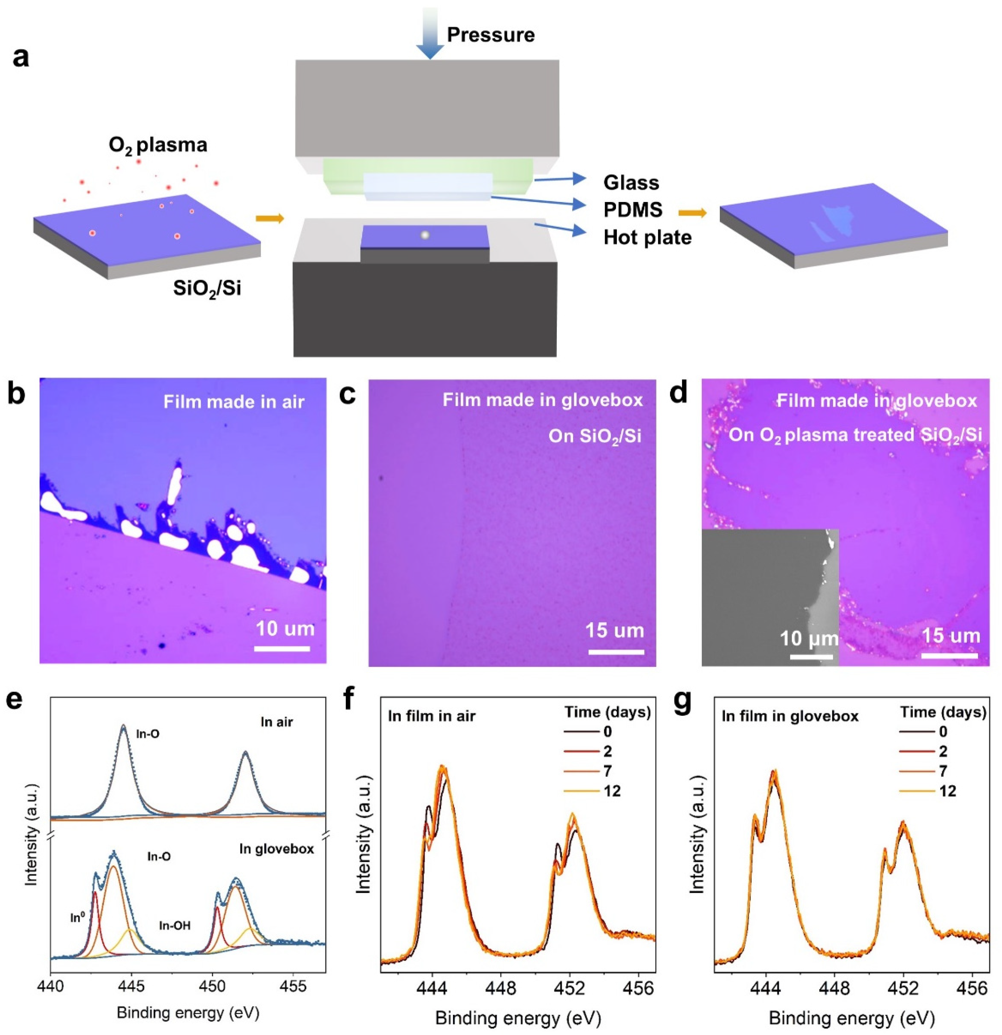
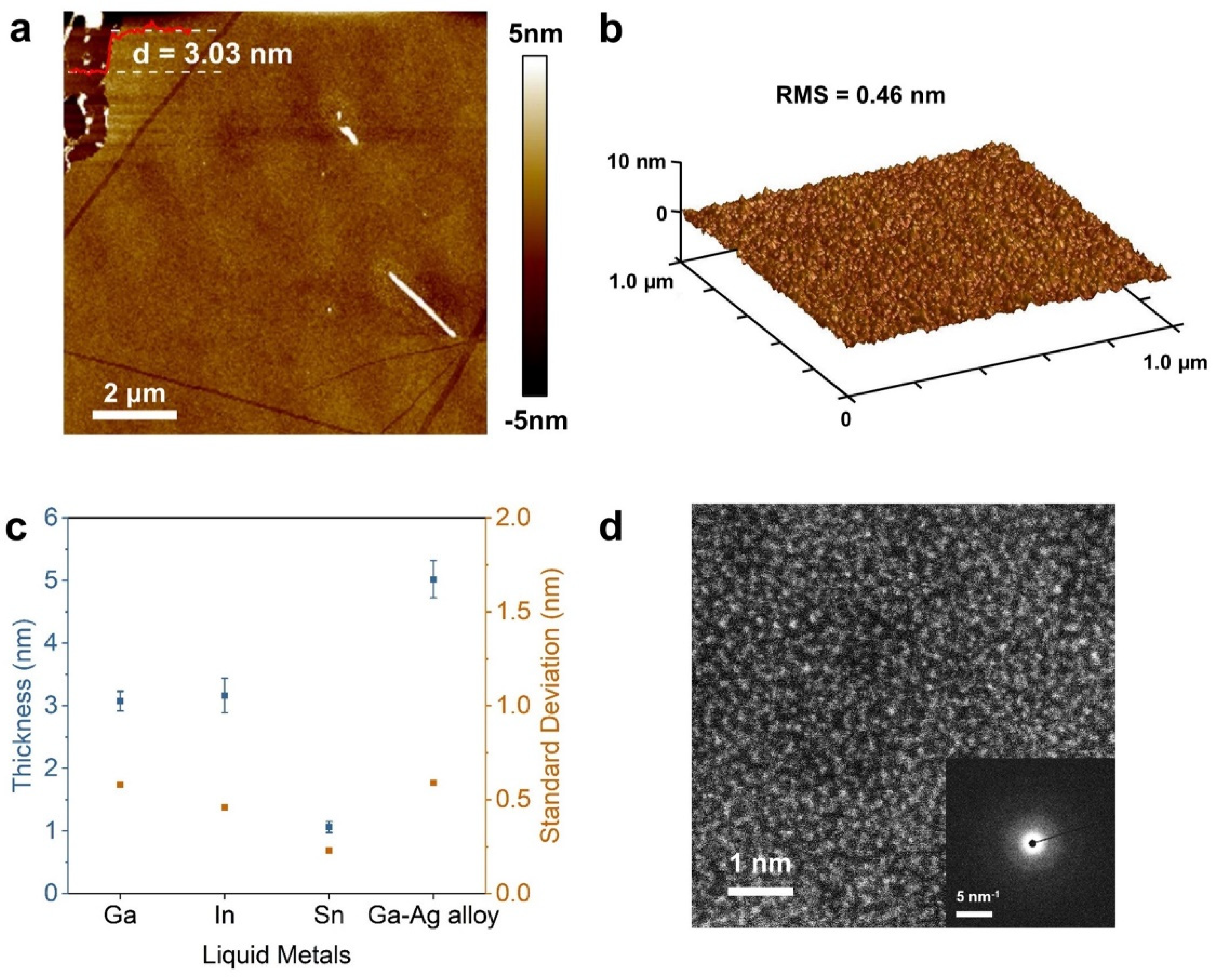
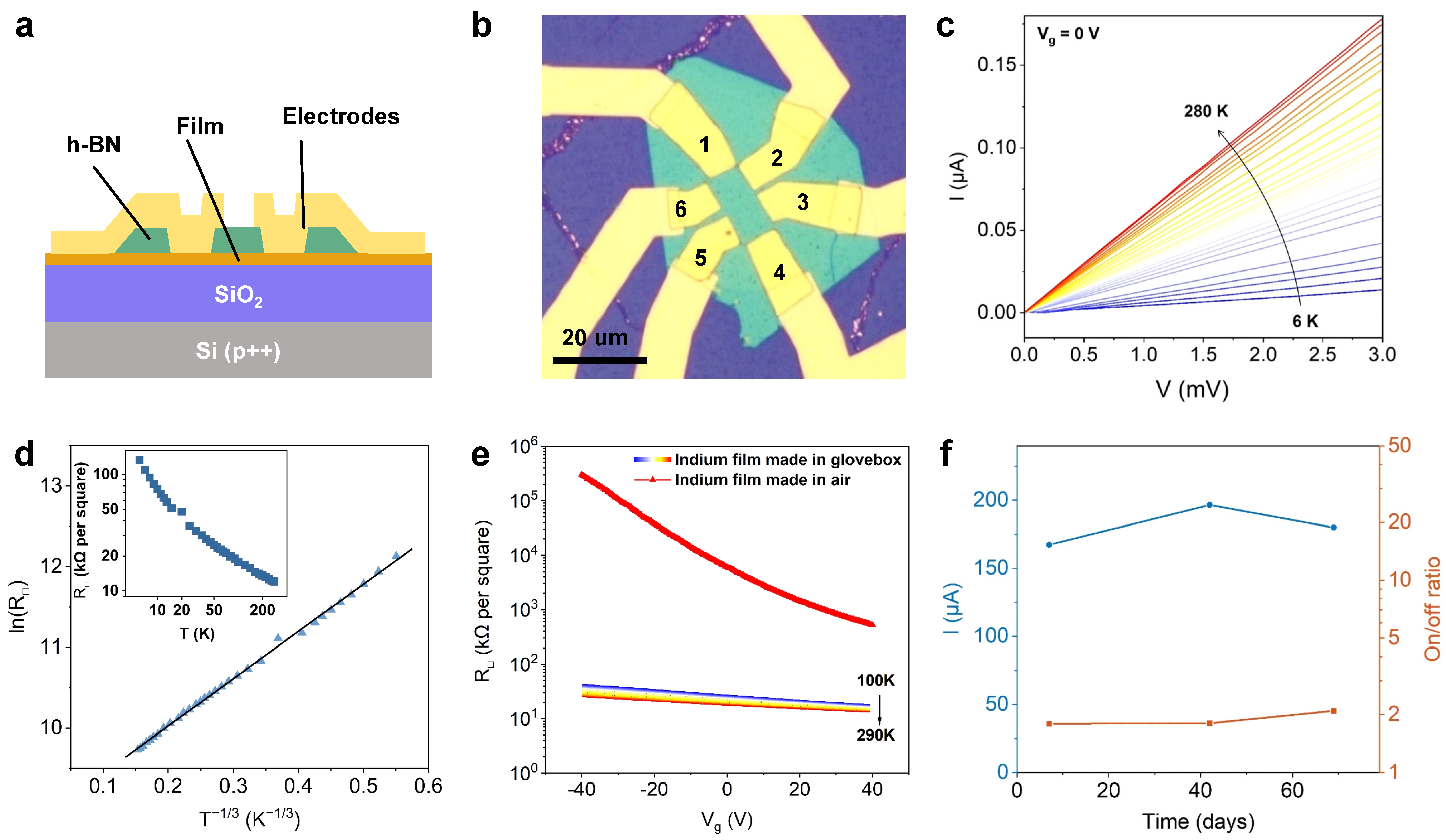
2. Results and Discussion

The fabrication process of 2D metal films is depicted in Figure 1a. First, metal particles were placed on O2 plasma-pretreated substrates in glovebox and then heated above their melting temperatures to obtain liquid metal droplets. Next, these liquid metal droplets on SiO2/Si substrate were pressed by PDMS/glass in a homemade hot-pressing machine. Finally, 2D metal films were formed on SiO2(300 nm)/Si substrate. See Section 3 for more details.
Typically, large-area homogeneous metal films can be easily formed in air by this hot-pressing method (Figure 1b) since the liquid metal drops have low surface energy in air due to the surface oxidation. Such freshly made metal films are not stable in air and easily oxidized. In order to minimize oxidation, we then performed hot-pressing processes in glovebox. However, the surface energy of liquid metal drops is extremely high in vacuum or inert environments, leading to a poor adhesion force between metals and substrates. As a result, only discrete metal particles can be obtained on the SiO2/Si substrate after hot-pressing in glovebox (Figure 1c). Here we used O2 plasma treatments of substrate surface to improve the adhesion between liquid metal drops and SiO2/Si substrates. Usually, O2 plasma treatment of substrates is used for dry etching and surface modification, especially for turning hydrophobic surfaces into hydrophilic ones [25]. It is believed that O2 plasma treatment can increase the density of Si–O and Si–OH bonds on the SiO2 surface, thereby decreasing the surface energy of metal drops on the substrate. Contact angles between liquid Bi drops and SiO2/Si substrate with or without O2 plasma treatments show obvious differences (Figure S1). Figure 1d presents the as-obtained large-area continuous and homogeneous In film made in glovebox on O2 plasma-pretreated SiO2/Si substrates.
The chemical states of In films were investigated by XPS (Figure 1e). In control samples made in air, two peaks centered at 444.5 and 452.0 eV are seen, confirming the complete oxidation of the In films. In contrast, samples made in glovebox show the In 3 d 5 / 2 peaks at a binding energy of 443.3, 444.3, and 445.3 eV, corresponding to metal In, In2O3, and indium hydroxyl species, respectively [26,27,28]. The oxidation is possibly due to the remaining oxygen on the substrate. The indium hydroxyl species are attributed to hydroxyl groups absorbed on the substrate surface. As for Ga films, the peaks centered at 18.5 and 20.0 eV corresponding to metal Ga and Ga3+(Ga2O3), respectively (Figure S2a). The comparison between Ga films made in air and in glovebox suggests that Ga films made in glovebox are less oxidized than those made in air. In addition to Ga and In films, more metal films were synthesized by this hot-pressing method, as illustrated in Figures S3 and S4. These films are also continuous and homogeneous with a scale of at least tens of microns and partially oxidized as indicated by the XPS results (Figure S2). The stability of In films in the air and glovebox are examined by XPS. The XPS peaks corresponding to metal In (Figure 1f) showed continuous decreased intensity during 12 days of storage in air, while the same peak showed nearly no change after 12 days of storage in glovebox (Figure 1g). This demonstrates that In film is only stable in oxygen-free environment such as glovebox. The same is true of Ga film (Figure S5a,e).
In order to further characterize the thickness and roughness of as-obtained metal films, we performed in situ Atomic force microscopy (AFM) measurements in glovebox. Figure 2a,b show a typical ultrathin In film with a thickness of ~3.0 nm and a surface roughness of ~0.46 nm. After checking many different samples, the thinnest metals we could obtain were plotted in Figure 2c and Figure S6. Depending on the different metals, the thinnest thickness varies from 1.1 to 5.0 nm, and the roughness falls between 0.2 nm (Sn film) and 0.6 nm (Ga0.87Ag0.13 film), comparable with that of the substrate (~0.27 nm). The comparatively large roughness of Ga and Ga0.87Ag0.13 films is attributed to the little Ga and Ag particles dispersed in those films (Figure S6a,c), due to the agglomeration of residual liquid metals. This situation of residual metal droplets also occurred in solid–melt exfoliation [23]. The PDMS-assisted hot-pressing method can effectively increase the flatness of films. The crystallinity of 3.1 nm thick Ga film was then examined by electron diffraction and high-resolution STEM image in Figure 2d, and the ring halo pattern in the diffraction image verified the amorphous nature of the Ga film. Raman spectrum (Figure S7) of all films showed no additional Raman peak compared to the Raman spectrum of the substrate, suggesting the lack of crystalline structure in the films. X-ray diffraction (XRD) (Figure S8) spectra of all films have no sharp and strong peaks and also confirmed the amorphous structure of the films.
We further fabricated three-terminal devices based on as-obtained In and Ga films to investigate their transport properties. Due to their instability in air, the as-obtained films would be contaminated during the commonly used device fabrication process. In particular, unencapsulated devices based on Ga film show extremely large resistance of ~TΩ, demonstrating an insulating behavior similar to Ga2O3 [22]. Therefore, a method of transfer via contact in glovebox was performed before lithography procedures in air to avoid contamination or additional oxidization [29]. Figure 3a illustrates the device structure in which the metal film is encapsulated by h-BN and contacted with gold (see detailed fabrication process in Section 3 and Figure S9). Four-probe electronic transport measurements were performed at various temperatures. I–V curves of a typical 5 nm thick In film device at temperatures varying from 6 to 280 K are shown in Figure 3c, exhibiting linear characteristics with sheet resistances of ~10 kΩ at room temperature. Temperature-dependent R behavior (Figure 3d) extracted from Figure 3c is in agreement with Mott’s law ρ = ρ0 exp[(T0/T)1/3] for 2D VRH mechanisms [30]. Similar R–T behavior was also observed in 4 nm thick Ga film devices (Figure S10). The devices exhibit resistances larger than 10 kΩ, falling into a strongly disordered regime [31]. This electronic transport behavior is believed to originate from the hopping mechanism caused by defects and disordered atom arrangements in the amorphous metal films. Mott’s 2D VRH has been observed in various systems with different origins of disorders, such as intergrain hopping and localized gap states [32,33,34]. In MoS2 nanoflakes, the R–T behavior changes from thermally activated transport at high temperatures to the Mott’s 2D VRH transport at low temperatures [35]. Our films, on the other hand, exhibit Mott’s 2D VRH transport across the measured temperature, indicating the dominance of disorder in this system. Further measurements are needed for the determination of the localization length, the hopping distance, and the hopping energy. Our work, for the first time, observed the Mott’s 2D VRH behavior among amorphous metal films with nanometer thickness.
So far, thin films of low-melting-point metals and alloys can be synthesized by various approaches [11,12,13,16,19,20,21,22,23,24,36,37]. In these materials, superconductivity [12,13], p-/n-type semiconductors [20,21,37], or insulators [22] have been observed (Table 1). However, the transport behavior of few nanometer-thick amorphous metal films has been rarely investigated. It is well known that In2O3 is an n-type semiconductor with a direct bandgap of 3.6 eV [38]. Transistors based on amorphous In2O3 have been fabricated with a mobility of 15 cm2 V−1 s−1 and an on/off ratio of 106 [39]. In our In films obtained in glovebox, the sheet resistances R showed very weak dependence on Vg, as shown in Figure 3e. The on/off ratio of the device was 1.90~2.37 at temperatures varying from 100 to 290 K, suggesting a metallic nature of the as-obtained In films. In contrast, devices fabricated from In films made in air displayed significantly larger sheet resistance and an on/off ratio of 103. The increase in sheet resistance and on/off ratio were attributed to the high oxidation degree of In films made in air, leading to their semiconducting behavior. In addition, the metallic behaviors of our encapsulated In films also persisted after 70 days in ambient conditions (Figure 3f), verifying great stability of In devices. The conversion of transport behavior from metallic to semiconducting provides us with a new degree of freedom to manipulate 2D materials, which can be realized by changing the oxygen concentration of the synthesis environment.

3. Methods

3.1. Fabrication of Metal Films in Glovebox

At first, SiO2 substrate was treated with O2 plasma under 150 W for 30 min. Then, low-melting-point metal pellets (Ga, In, Sn, and Ga0.87Ag0.13) were placed on substrate and heated to temperatures above their melting point (50, 180, 260, and 300 ℃, respectively) in glovebox until they were completely melted. By pressing metal drops with PDMS under the pressure of 100 kPa, we obtained metal films on SiO2 (300 nm)/Si substrate. The PDMS was prepared using SYLGARD 184 (Dow Corning Corporation), two-part kit consisting of prepolymer (base), and cross-linker (curing agent). We mixed the prepolymer and cross-linker at a 10:1 weight ratio and cured PDMS films on glass slide at 80 °C for 2 h. During the hot-pressing process, the use of soft PDMS was beneficial for offering uniform pressure exerted on the sample. In addition, the weak adhesion between metal films and PDMS made it easy to detach PDMS from metal films after the hot-pressing process.

3.2. Characterizations

AFM topography was measured by ScanAsyst mode using a Bruker Multimode 8 system. SEM images were acquired using JEM-IT500 InTouchScope scanning electron microscope. XPS spectra were measured with a Thermo Fisher ESCALAB XI+ with Monochromatic Al Kα X-ray (photon energy of 1480.6 eV). The emitted photoelectrons were collected to the analyzer at 90° to the surface of the sample. The Raman spectra were acquired from a Horiba Jobin Yvon Lab RAM HR-Evolution Raman system with a 532 nm He–Ne laser (spot size ≈ 2 μm, power 1 mW, and accumulation time 120 s). XRD spectra were acquired with an X-ray diffractometer (Empyrean) using grazing incidence XRD.
For TEM characterizations, the samples were picked up by h-BN on PPC and then transferred onto TEM microgrid. SAED was performed with a TEM (JEOL JEM-F200) operating at 200 kV, whereas high-resolution STEM was performed with a spherical aberration corrected TEM (JEM-ARM200F) operating at 200 kV.

3.3. Device Fabrication and Electronic Measurements

The fabrication of three-terminal devices consisted of two procedures: First there was the preparation of h-BN-encapsulated electrodes and transferring inside a glovebox. Second was the patterning of electrode pads and etching of extra metal film outside channel regions. The h-BN flake of a thickness between 25 and 35 nm was exfoliated on clean SiO2 substrate and patterned using EBL lithography and RIE etching to form contact voids. Then we used E-beam evaporator to evaporate 40 nm thick Au electrodes to cover the aforementioned h-BN voids. We used PPC supported by PDMS on a glass slide to pick up the as-prepared structure and transfer it onto metal film in glovebox. Last, the device was wired out by Ti (2 nm)/Au (40 nm) electrodes, and extra metal film outside channel regions was etched using EBL and argon plasma etching. The transfer characteristic measurements were carried out with an Agilent 4156C semiconductor parameter analyzer under 3 × 10⁻⁶ mbar high vacuum four-probe station system. The four-probe R–T measurements were performed in cryostat with a base temperature of 1.5 K, an Agilent B1500 semiconductor parameter analyzer, and a Keithley 2000 source meter.

4. Conclusions

In summary, we proposed a PDMS-assisted hot-pressing method to synthesize ultrathin amorphous films of low-melting-point metals and alloys, such as Ga, In, Sn, and Ga0.87Ag0.13. The R–T behavior of three-terminal devices based on In film fits with Mott’s 2D VRH model. It is worth mentioning that during the device fabrication process, transfer via contact method in glovebox was used to avoid oxidation or degradation of metal films, and this transfer method can be applied to other 2D materials. Our film producing method and device fabricating technology provide a novel approach for the study of intrinsic properties of 2D metals or metal oxides.

Supplementary Materials

The following supplementary materials can be downloaded at: https://www.mdpi.com/article/10.3390/cryst12050616/s1, Figure S1: Contact angles between Bi drops and substrate before and after O2 plasma treatment; Figure S2: XPS spectra of 2D films made of Ga, Sn, and Ga0.87Ag0.13 alloy synthesized in air and glovebox; Figure S3: Optical images of 2D films made of Ga, Sn, and Ga0.87Ag0.13 alloy; Figure S4: SEM images of 2D films made of Ga, Sn, and Ga0.87Ag0.13 alloy; Figure S5: The variation of XPS spectrum of films made in glovebox and then stored in air and in glovebox for 12 days; Figure S6: AFM images of 2D films made of Ga, Sn, and Ga0.87Ag0.13 alloy; Figure S7: Raman spectrum of 2D films made of Ga, Sn, and Ga0.87Ag0.13 alloy; Figure S8: XRD spectra of 2D films made of Ga, Sn, and Ga0.87Ag0.13 alloy; Figure S9: Fabrication process of h-BN-encapsulated electrode; Figure S10: Electronic properties of Ga film.

Author Contributions

Conceptualization, G.Z.; Data curation, J.L. (Jieying Liu) and G.L.; Formal analysis, J.L. (Jieying Liu) and J.T. (Jian Tang); Funding acquisition, D.S. and G.Z.; Investigation, (J.L.) (Jieying Liu), J.T. (Jian Tang), J.Z. and S.W.; Methodology, J.L. (Jieying Liu), Y.Z., M.L., J.T. (Jinpeng Tian), Y.C., J.L. (Jiawei Li) and Z.W.; Project administration, G.Z.; Supervision, G.Z.; Validation, J.L. (Jieying Liu), C.S., G.L., W.Y., R.Y., N.L., D.S. and G.Z.; Writing—original draft, J.L.; Writing—review & editing, N.L. and G.Z. All authors have read and agreed to the published version of the manuscript.

Funding

This research was funded by the Key-Area Research and Development Program of Guangdong Province (Grant No. 2020B0101340001), the National Natural Science Foundation of China (NSFC, Grant Nos. 61888102, 11834017, 62122084, 12074412, and 12104330), the Strategic Priority Research Program of Chinese Academy of Sciences (CAS, Grant No. XDB30000000), and the National Key R&D Program of China (Grant No. 2020YFA0309600).

Institutional Review Board Statement

Not applicable.

Informed Consent Statement

Not applicable.

Data Availability Statement

The data that support the findings of this study are available from the corresponding author upon reasonable request.

Conflicts of Interest

The authors declare no conflict of interest.

References

  1. Novoselov, K.S.; Geim, A.K.; Morozov, S.V.; Jiang, D.; Zhang, Y.; Dubonos, S.V.; Grigorieva, I.V.; Firsov, A.A. Electric Field Effect in Atomically Thin Carbon Films. Science 2004, 306, 666–669. [Google Scholar] [CrossRef] [PubMed] [Green Version]
  2. Tan, C.; Cao, X.; Wu, X.-J.; He, Q.; Yang, J.; Zhang, X.; Chen, J.; Zhao, W.; Han, S.; Nam, G.-H.; et al. Recent Advances in Ultrathin Two-Dimensional Nanomaterials. Chem. Rev. 2017, 117, 6225–6331. [Google Scholar] [CrossRef] [PubMed]
  3. Pei, Y.; Huang, L.; Wang, J.; Han, L.; Li, S.; Zhang, S.; Zhang, H. Recent Progress in the Synthesis and Applications of 2D Metal Nanosheets. Nanotechnology 2019, 30, 222001. [Google Scholar] [CrossRef] [PubMed]
  4. Kumbhakar, P.; Chowde Gowda, C.; Mahapatra, P.L.; Mukherjee, M.; Malviya, K.D.; Chaker, M.; Chandra, A.; Lahiri, B.; Ajayan, P.M.; Jariwala, D.; et al. Emerging 2D Metal Oxides and Their Applications. Mater. Today 2021, 45, 142–168. [Google Scholar] [CrossRef]
  5. Daeneke, T.; Khoshmanesh, K.; Mahmood, N.; de Castro, I.A.; Esrafilzadeh, D.; Barrow, S.J.; Dickey, M.D.; Kalantar-zadeh, K. Liquid Metals: Fundamentals and Applications in Chemistry. Chem. Soc. Rev. 2018, 47, 4073–4111. [Google Scholar] [CrossRef] [PubMed]
  6. Zhao, S.; Zhang, J.; Fu, L. Liquid Metals: A Novel Possibility of Fabricating 2D Metal Oxides. Adv. Mater. 2021, 33, 2005544. [Google Scholar] [CrossRef]
  7. Huang, K.; Hou, J.; Zhang, Q.; Ou, G.; Ning, D.; Hussain, N.; Xu, Y.; Ge, B.; Liu, K.; Wu, H. Ultrathin Two-Dimensional Metals with Fully Exposed (111) Facets. Chem. Commun. 2018, 54, 160–163. [Google Scholar] [CrossRef]
  8. Lin, Z.; Du, C.; Yan, B.; Wang, C.; Yang, G. Two-Dimensional Amorphous NiO as a Plasmonic Photocatalyst for Solar H2 Evolution. Nat. Commun. 2018, 9, 4036. [Google Scholar] [CrossRef] [Green Version]
  9. Dral, A.P.; ten Elshof, J.E. 2D Metal Oxide Nanoflakes for Sensing Applications: Review and Perspective. Sens. Actuators B Chem. 2018, 272, 369–392. [Google Scholar] [CrossRef] [Green Version]
  10. Datta, R.S.; Syed, N.; Zavabeti, A.; Jannat, A.; Mohiuddin, M.; Rokunuzzaman, M.; Zhang, B.Y.; Rahman, M.A.; Atkin, P.; Messalea, K.A.; et al. Flexible Two-Dimensional Indium Tin Oxide Fabricated Using a Liquid Metal Printing Technique. Nat. Electron. 2020, 3, 51–58. [Google Scholar] [CrossRef]
  11. Yang, F.; Miao, L.; Wang, Z.F.; Yao, M.-Y.; Zhu, F.; Song, Y.R.; Wang, M.-X.; Xu, J.-P.; Fedorov, A.V.; Sun, Z.; et al. Spatial and Energy Distribution of Topological Edge States in Single Bi(111) Bilayer. Phys. Rev. Lett. 2012, 109, 016801. [Google Scholar] [CrossRef] [PubMed] [Green Version]
  12. Briggs, N.; Bersch, B.; Wang, Y.; Jiang, J.; Koch, R.J.; Nayir, N.; Wang, K.; Kolmer, M.; Ko, W.; De La Fuente Duran, A.; et al. Atomically Thin Half-van Der Waals Metals Enabled by Confinement Heteroepitaxy. Nat. Mater. 2020, 19, 637–643. [Google Scholar] [CrossRef] [PubMed]
  13. Zhang, H.M.; Sun, Y.; Li, W.; Peng, J.P.; Song, C.L.; Xing, Y.; Zhang, Q.; Guan, J.; Li, Z.; Zhao, Y.; et al. Detection of a Superconducting Phase in a Two-Atom Layer of Hexagonal Ga Film Grown on Semiconducting GaN(0001). Phys. Rev. Lett. 2015, 114, 107003. [Google Scholar] [CrossRef] [PubMed] [Green Version]
  14. Fickert, M.; Assebban, M.; Canet-Ferrer, J.; Abellán, G. Phonon Properties and Photo-Thermal Oxidation of Micromechanically Exfoliated Antimonene Nanosheets. 2D Mater. 2021, 8, 015018. [Google Scholar] [CrossRef]
  15. Guo, Y.; Zhang, Y.-F.; Bao, X.-Y.; Han, T.-Z.; Tang, Z.; Zhang, L.-X.; Zhu, W.-G.; Wang, E.G.; Niu, Q.; Qiu, Z.Q.; et al. Superconductivity Modulated by Quantum Size Effects. Science 2004, 306, 1915–1917. [Google Scholar] [CrossRef]
  16. Reis, F.; Li, G.; Dudy, L.; Bauernfeind, M.; Glass, S.; Hanke, W.; Thomale, R.; Schäfer, J.; Claessen, R. Bismuthene on a SiC Substrate: A Candidate for a High-Temperature Quantum Spin Hall Material. Science 2017, 357, 287–290. [Google Scholar] [CrossRef] [Green Version]
  17. Xu, R.; Xie, T.; Zhao, Y.; Li, Y. Single-Crystal Metal Nanoplatelets:  Cobalt, Nickel, Copper, and Silver. Cryst. Growth Des. 2007, 7, 1904–1911. [Google Scholar] [CrossRef]
  18. Lim, B.S.; Rahtu, A.; Gordon, R.G. Atomic Layer Deposition of Transition Metals. Nat. Mater. 2003, 2, 749–754. [Google Scholar] [CrossRef]
  19. Hussain, N.; Liang, T.; Zhang, Q.; Anwar, T.; Huang, Y.; Lang, J.; Huang, K.; Wu, H. Ultrathin Bi Nanosheets with Superior Photoluminescence. Small 2017, 13, 1701349. [Google Scholar] [CrossRef]
  20. Messalea, K.A.; Carey, B.J.; Jannat, A.; Syed, N.; Mohiuddin, M.; Zhang, B.Y.; Zavabeti, A.; Ahmed, T.; Mahmood, N.; Della Gaspera, E.; et al. Bi2O3 Monolayers from Elemental Liquid Bismuth. Nanoscale 2018, 10, 15615–15623. [Google Scholar] [CrossRef]
  21. Daeneke, T.; Atkin, P.; Orrell-Trigg, R.; Zavabeti, A.; Ahmed, T.; Walia, S.; Liu, M.; Tachibana, Y.; Javaid, M.; Greentree, A.D.; et al. Wafer-Scale Synthesis of Semiconducting SnO Monolayers from Interfacial Oxide Layers of Metallic Liquid Tin. ACS Nano 2017, 11, 10974–10983. [Google Scholar] [CrossRef] [PubMed]
  22. Li, J.; Zhang, X.; Yang, B.; Zhang, C.; Xu, T.; Chen, L.; Yang, L.; Jin, X.; Liu, B. Template Approach to Large-Area Non-Layered Ga-Group Two-Dimensional Crystals from Printed Skin of Liquid Gallium. Chem. Mater. 2021, 33, 4568–4577. [Google Scholar] [CrossRef]
  23. Kochat, V.; Samanta, A.; Zhang, Y.; Bhowmick, S.; Manimunda, P.; Asif, S.A.S.; Stender, A.S.; Vajtai, R.; Singh, A.K.; Tiwary, C.S.; et al. Atomically Thin Gallium Layers from Solid-Melt Exfoliation. Sci. Adv. 2018, 4, e1701373. [Google Scholar] [CrossRef] [PubMed] [Green Version]
  24. Zavabeti, A.; Ou, J.Z.; Carey, B.J.; Syed, N.; Orrell-Trigg, R.; Mayes, E.L.H.; Xu, C.; Kavehei, O.; O’Mullane, A.P.; Kaner, R.B.; et al. A Liquid Metal Reaction Environment for the Room-Temperature Synthesis of Atomically Thin Metal Oxides. Science 2017, 358, 332–335. [Google Scholar] [CrossRef] [Green Version]
  25. Bazaka, K.; Baranov, O.; Cvelbar, U.; Podgornik, B.; Wang, Y.; Huang, S.; Xu, L.; Lim, J.W.M.; Levchenko, I.; Xu, S. Oxygen Plasmas: A Sharp Chisel and Handy Trowel for Nanofabrication. Nanoscale 2018, 10, 17494–17511. [Google Scholar] [CrossRef]
  26. Dang, M.T.; Wantz, G.; Hirsch, L.; Wuest, J.D. Recycling Indium Tin Oxide (ITO) Anodes for Use in Organic Light-Emitting Diodes (OLEDs). Thin Solid Films 2017, 638, 236–243. [Google Scholar] [CrossRef]
  27. Shinde, D.V.; Ahn, D.Y.; Jadhav, V.V.; Lee, D.Y.; Shrestha, N.K.; Lee, J.K.; Lee, H.Y.; Mane, R.S.; Han, S.H. A Coordination Chemistry Approach for Shape Controlled Synthesis of Indium Oxide Nanostructures and Their Photoelectrochemical Properties. J. Mater. Chem. A 2014, 2, 5490–5498. [Google Scholar] [CrossRef]
  28. Zatsepin, D.A.; Boukhvalov, D.W.; Zatsepin, A.F.; Vines, L.; Gogova, D.; Shur, V.Y.; Esin, A.A. Bulk In2O3 Crystals Grown by Chemical Vapour Transport: A Combination of XPS and DFT Studies. J. Mater. Sci. Mater. Electron. 2019, 30, 18753–18758. [Google Scholar] [CrossRef]
  29. Jung, Y.; Choi, M.S.; Nipane, A.; Borah, A.; Kim, B.; Zangiabadi, A.; Taniguchi, T.; Watanabe, K.; Yoo, W.J.; Hone, J.; et al. Transferred via Contacts as a Platform for Ideal Two-Dimensional Transistors. Nat. Electron. 2019, 2, 187–194. [Google Scholar] [CrossRef]
  30. Mott, N.F. Conduction in Non-Crystalline Materials: III. Localized States in a Pseudogap and near Extremities of Conduction and Valence Bands. Philos. Mag. 1969, 19, 835–852. [Google Scholar] [CrossRef]
  31. Bishop, D.J.; Tsui, D.C.; Dynes, R.C. Nonmetallic Conduction in Electron Inversion Layers at Low Temperatures. Phys. Rev. Lett. 1980, 44, 1153–1156. [Google Scholar] [CrossRef]
  32. Qiu, H.; Xu, T.; Wang, Z.; Ren, W.; Nan, H.; Ni, Z.; Chen, Q.; Yuan, S.; Miao, F.; Song, F.; et al. Hopping Transport through Defect-Induced Localized States in Molybdenum Disulphide. Nat. Commun. 2013, 4, 2642. [Google Scholar] [CrossRef] [PubMed]
  33. Lai, J.J.; Jian, D.; Lin, Y.F.; Ku, M.M.; Jian, W.B. Electron Transport in the Two-Dimensional Channel Material—Zinc Oxide Nanoflake. Phys. B Condens. Matter 2018, 532, 135–138. [Google Scholar] [CrossRef]
  34. Long, G.; Xu, S.; Cai, X.; Wu, Z.; Han, T.; Lin, J.; Cheng, C.; Cai, Y.; Wang, X.; Wang, N. Gate-Tunable Strong-Weak Localization Transition in Few-Layer Black Phosphorus. Nanotechnology 2018, 29, 035204. [Google Scholar] [CrossRef] [PubMed] [Green Version]
  35. Xue, J.; Huang, S.; Wang, J.Y.; Xu, H.Q. Mott Variable-Range Hopping Transport in a MoS2 Nanoflake. RSC Adv. 2019, 9, 17885–17890. [Google Scholar] [CrossRef] [Green Version]
  36. Yang, Z.; Wu, Z.; Lyu, Y.; Hao, J. Centimeter-Scale Growth of Two-Dimensional Layered High-Mobility Bismuth Films by Pulsed Laser Deposition. InfoMat 2019, 1, 98–107. [Google Scholar] [CrossRef] [Green Version]
  37. Zhu, F.; Chen, W.; Xu, Y.; Gao, C.; Guan, D.; Liu, C.; Qian, D.; Zhang, S.-C.; Jia, J. Epitaxial Growth of Two-Dimensional Stanene. Nat. Mater. 2015, 14, 1020–1025. [Google Scholar] [CrossRef]
  38. Ismail, R.A.; Abdulrazaq, O.A.; Yahya, K.Z. Preparation and Characterization of In2O3 Thin Films for Optoelectronic Applications. Surf. Rev. Lett. 2005, 12, 515–518. [Google Scholar] [CrossRef]
  39. Jiao, Y.; Zhang, X.; Zhai, J.; Yu, X.; Ding, L.; Zhang, W. Bottom-Gate Amorphous In2O3 Thin Film Transistors Fabricated by Magnetron Sputtering. Electron. Mater. Lett. 2013, 9, 279–282. [Google Scholar] [CrossRef]
  40. Liu, H.; Tang, H.; Fang, M.; Si, W.; Zhang, Q.; Huang, Z.; Gu, L.; Pan, W.; Yao, J.; Nan, C.; et al. 2D Metals by Repeated Size Reduction. Adv. Mater. 2016, 28, 8170–8176. [Google Scholar] [CrossRef]
Figure 1. (a) Process diagram of fabricating 2D metal/metal oxide films. Optical images of In films made (b) in air, (c) in glovebox on SiO2 (300 nm)/Si substrate, and (d) in glovebox on O2 plasma-pretreated SiO2/Si substrate. Inset of (d) shows scanning electron microscope (SEM) image of corresponding sample. (e) XPS spectra of In 3d in In films made in air (top panel) and in glovebox (bottom panel). (f,g) The variation of XPS spectra of In 3d from In films made in glovebox and then stored in air (f) and in glovebox (g) for 12 days.
Crystals 12 00616 g001
Figure 2. AFM images showing thickness (a) and roughness (b) of In film made in glovebox. (c) Summary of thicknesses and surface roughness of Ga, In, Sn, and Ga0.87Ag0.13 alloy films. (d) High-resolution STEM image of Ga film, inset is the selected area electron diffraction (SAED).
Crystals 12 00616 g002
Figure 3. Electronic properties of three-terminal devices based on In film. (a) Schematic of the device structure; (b) Optical image of the fabricated devices; (c) I–V curves of the device at various temperatures; (d) The relationship of sheet resistance R and T fitted by 2D Mott’s VRH model; inset shows R versus T plotted in double logarithmic scale; (e) Comparison of R versus gate voltage curves for In film made in air and in glovebox; (f) On/off ratio and current of In device after 2 months of exposure in air.
Crystals 12 00616 g003
Table 1. Summary of representative 2D metal and metal oxide film fabrication methods.
Ref.MaterialProcessing Temperature [°C]MethodThickness [nm]Oxidation DegreeCrystallinityElectrical Properties
[40]Ag, Au, FeRT aMechanical rolling method1~5MetalPolycrystal (Ag)N/A
[17]Co, Ni, Cu, Ag100~110Hydro/solvothermal~8MetalCrystalN/A
[14]SbRT aMechanical exfoliation>14Metal SbCrystalN/A
[15]PbN/AMBE12~28 layersMetal Pb on Si(111)CrystalSC b
[36]Bi100PLD1~15 Metal Bi(111) on SiO2(300nm)/SiCrystalP-type
[19]Bi150Hot-pressing2~10Metal BiCrystalN/A
[20]Bi300Squeeze transfer0.75α-Bi2O3CrystalN-type semiconductor
[11]BiN/AMBEBilayerMetal Bi on Bi2Te3CrystalN/A
[16]BiN/AMBEMonolayerMetal Bi(111) on SiCCrystalN/A
[21]Sn300Squeeze transfer~0.6SnO and SnO2PolycrystalP-type semiconductor
[37]SnN/AMBE1~3 layers Metal Sn on Bi2Te3(111)α-Sn(111)N/A
[22]Ga50, 800PDMS-printing strategy and heat treatment~6β-Ga2O3PolycrystalInsulator
[23]Ga50Solid-melt exfoliation~4Metal GaCrystalConductor
[12]Ga700~800Confinement heteroepitaxyTrilayerMetal graphene/Ga/SiCSingle crystalSC b
InBilayerMetal graphene/In/SiCSingle crystalN/A
SnmonolayerMetal graphene/Sn/SiCSingle crystalN/A
[13]Ga650MBE0.552Metal Ga/GaN(0001)Single crystalSC b
[24]Galinstan, EGaInRT aGas-injection method5.2Ga2O3, AI2O3, Hf2O3, Gd2O3AmorphousN/A
This workGa50PDMS-hot-pressing~3.1Coexistence of metal Ga and Ga2O3AmorphousConductor, (Mott’s 2D VRH model)
In180~3.2Coexistence of metal In and In2O3N/AConductor, (Mott’s 2D VRH model)
Sn260~1.1Coexistence of SnO and SnO2N/AN/A
Ga0.87Ag0.13300~5Coexistence of metal Ga, Ag and Ga2O3N/AN/A
a Room temperature. b Superconductivity.
Publisher’s Note: MDPI stays neutral with regard to jurisdictional claims in published maps and institutional affiliations.

