Article

On-State Voltage Drop Analytical Model for 4H-SiC Trench IGBTs

1
The College of Electronic and Information Engineering, Shenyang Aerospace University, Shenyang 110136, China
2
School of Integrated Circuits, Tsinghua University, Beijing 100084, China
*
Author to whom correspondence should be addressed.
Crystals 2022, 12(5), 582; https://doi.org/10.3390/cryst12050582
Submission received: 11 March 2022 / Revised: 5 April 2022 / Accepted: 18 April 2022 / Published: 22 April 2022
(This article belongs to the Special Issue Wide Bandgap Semiconductor Electronics and Optoelectronics)

Abstract

:
In this paper, a model for the forward voltage drop in a 4H-SiC trench IGBT is developed. The analytical model is based on the 4H-SiC trench MOSFET voltage model and the hole-carrier concentration profile in the N-drift region for a conventional 4H-SiC trench IGBT. Moreover, an on-state voltage drop analytical model is validated using a 2D numerical simulation, and the simulation results demonstrate that there is good agreement between the ATLAS simulation data and analytic solutions.

1. Introduction

In recent years, power semiconductor devices based on 4H-SiC have attracted more attention due to the material’s high power and high temperature applications arising from its superior material properties [1,2,3,4]. Compared with SiC MOSFETs, SiC IGBTs can achieve a lower forward voltage drop when the blocking voltage is equal to or higher than 10 kV. Although the conductivity modulation effect makes the forward voltage drop lower, the turn-off loss is higher. Therefore, for IGBTs, there is conflict between the on-state voltage drop and turn-off loss. Many researchers have placed much emphasis on how to improve the trade-off relationship between the on-state voltage drop and the turn-off loss of 4H-SiC IGBTs [5,6,7,8,9,10,11,12,13], such as the adoption of the current storage layer (CSL) [10,11] and the proposed Cluster IGBT (CIGBT) [12,13].
While much research has been undertaken on how to improve the trade-off relationship [5,6,7,8,9,10,11,12,13], less work has been conducted on the analytical model and theoretical analysis of the static-state (forward voltage drop) and the dynamic-state (turn-off loss) [14,15,16]. In this paper, based on our previous findings [17,18,19], an on-state voltage drop analytical model for an n-channel 4H-SiC trench IGBT is developed. Additionally, a 2D numerical simulation using the ATLAS module of Silvaco TCAD [20] is utilized to validate the correctness of the proposed analytical model.

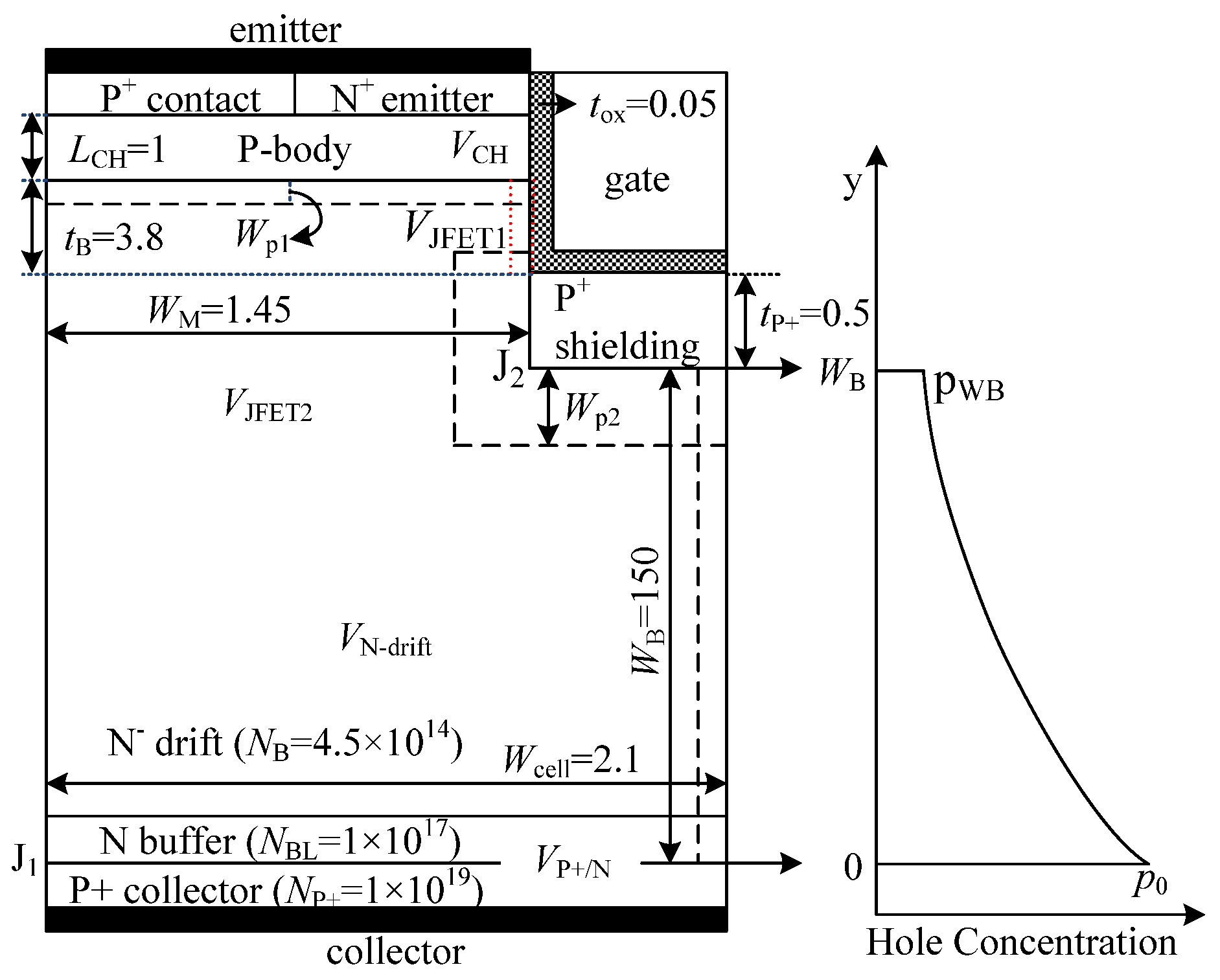
2. Forward Voltage Drop Analytical Model

The forward voltage drop (Von) of a 4H-SiC IGBT is composed of the upper MOS voltage part (VMOS), the N-type voltage blocking layer voltage (Vdrift), and the built-in potential at junction J1 (VP+N), which are shown on the left of Figure 1.
Firstly, the upper MOS voltage part includes three parts: the channel voltage (VCH), the parasitic JFET1 (composed of a P− body and P+ shielding) voltage (VJFET1), and the parasitic JFET2 (composed of P+ shielding in two close cells) voltage (VJFET2). Based on the existing 4H-SiC trench MOSFET voltage model, VCH, VJFET1, and VJFET2 can be calculated as:
V CH = J C R CH , sp = J C L CH W cell μ inv C ox ( V GE - V th ( on ) )
V JFET 1 = J C R JFET 1 , sp = J C ρ JFET 1 W cell ( t P + + W p 1 t B 2 W p 1 )
V JFET 2 = J C R JFET 2 = J C ρ JFET 2 W cell ( t P + + W p 2 W M W p 2 2 )
So, VMOS can be expressed [21] as:
V MOS = V CH + V JFET 1 + V JFET 2
where Cox is the specific capacitance of the gate oxide; μinv is the inversed electron mobility in channel region; ρ is the resistivity; VGE is the applied gate bias; Vth(on) is the threshold voltage; and Wp1 and Wp2 are the depletion length in the p-body/current storage layer (CSL) and P+ shielding/N-drift junction @ Vce = 0 V, respectively. Additionally, the Cox [21], ρ, and Wp1/2 can be written as:
C ox = ε oxide ε 0 t ox
ρ JFET 1 / 2 = 1 q n μ n = 1 q N CSL / B μ n
W p 1 / 2 = 2 ε SiC ε 0 V PN q N CSL / B
where εoxide and εSiC are the relative permittivity for the gate oxide and 4H-SiC; ε0 is the permittivity of free space; μn is the electron mobility; NCSL/B is the doping of CSL (or drift) region; q is the amount of electric charge of an electron; and VPN is the built-in potential of the PN junction (about 2.7 V).
Moreover, according to the formula of the PN junction built-in potential, VP+N can be calculated [22] as:
V P + N = k T q ln ( p 0 N BL n i 2 )
In Formula (8), k is the Boltzmann constant; T is the ambient temperature; ni is the intrinsic carrier concentration; NBL is the doping of the N buffer region; and p0 is the hole concentration at junction J1.
In order to simplify the analytical model of the voltage dropped on the N-type drift layer, the hole-carrier concentration, which is shown on the right of Figure 1, can be depicted as:
p ( y ) = Ae y L a + B
In (9), La is the ambipolar diffusion length; and p0 and pWB, which are the hole concentrations at P+ collector/N-buffer and P+ shielding/N-drift junctions, can be obtained using:
p 0 = p ( y ) | y = 0 = p ( 0 ) = p 0 , BL L p , BL L n , P + q ( D p , BL p 0 , BL L n , P + + D n , P + n 0 , P + L p , BL )
p W B = p ( y ) | y = W B = p ( W B ) = J C q v sat
in which p0,BL and n0,P+ are the hole and electron concentrations at a state of equilibrium; Dp,BL and Dn,P+ are the diffusion coefficients in the buffer layer and P+ collector region; Lp,BL and Ln,P+ are the diffusion lengths in the buffer layer and P+ collector region; JC is the total current density; and υsat is the drift velocity of the carriers.
If we replace Equations (10) and (11) into Equation (9), p(y) can be obtained.
By integrating an electric field across the N-type drift region, the N-drift region voltage can be calculated as:
V drift = 0 W B E ( y ) d y = 0 W B J p - drift q μ p p ( y ) d y
In (12), μp is the hole mobility, and Jp-drift is the hole current density flowing in the drift region, which is depicted as:
J p - drift = μ p μ p + μ n [ J C q ( μ n μ p 1 ) D p d p ( y ) d y ]
In (13), Dp is the hole diffusion coefficient.
If we replace Equation (13) into (12), Vdrift is changed as follows:
V drift = 0 W B J C q ( μ p + μ n ) p ( y ) + ( μ n μ p ) D p d p ( y ) d y μ p ( μ p + μ n ) p ( y ) d y = J C q ( μ p + μ n ) B ( W B + L a ln p ( W B ) p ( 0 ) ) + ( μ n μ p ) D p μ p ( μ p + μ n ) ln p ( W B ) p ( 0 )
Then, the forward voltage can be calculated.

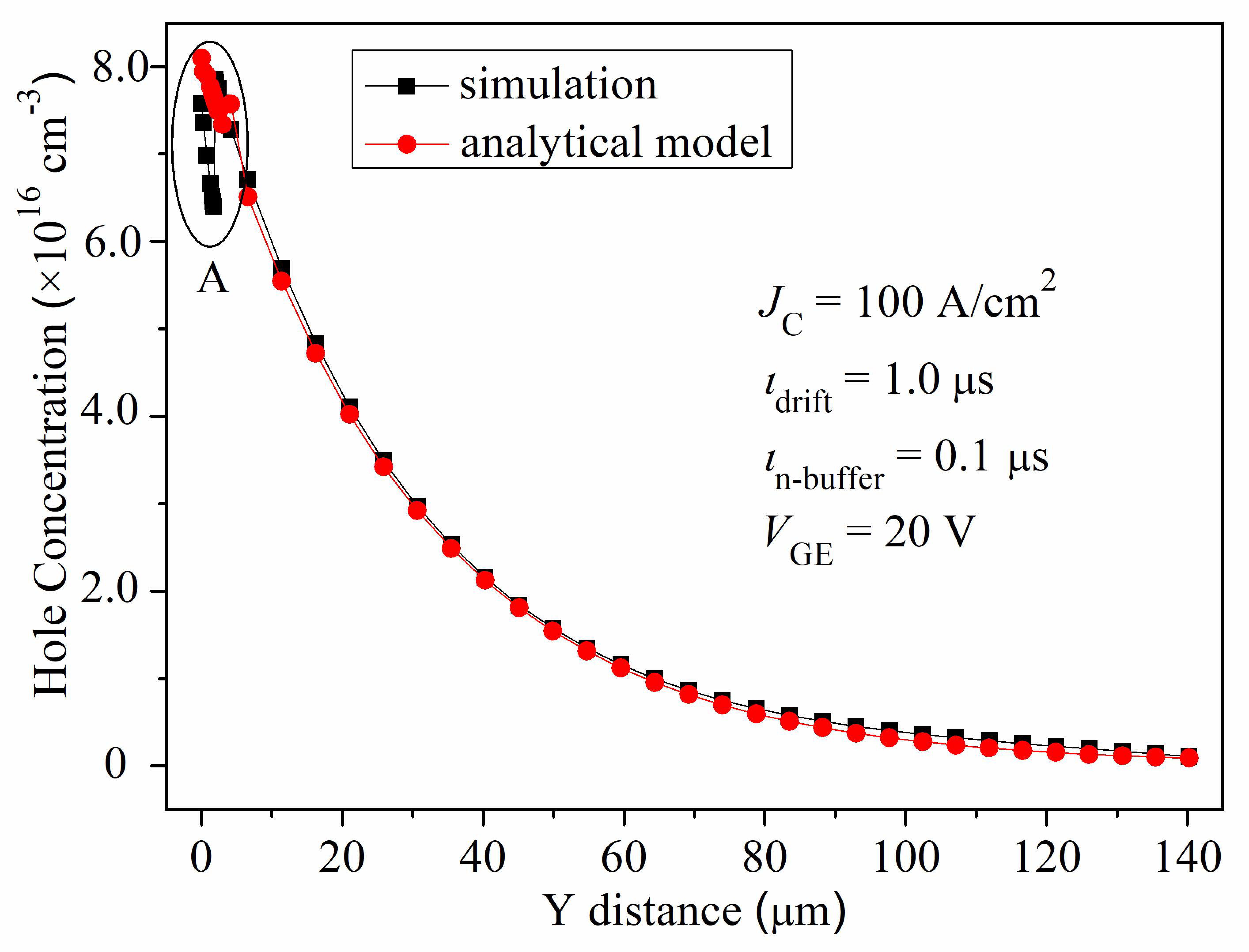
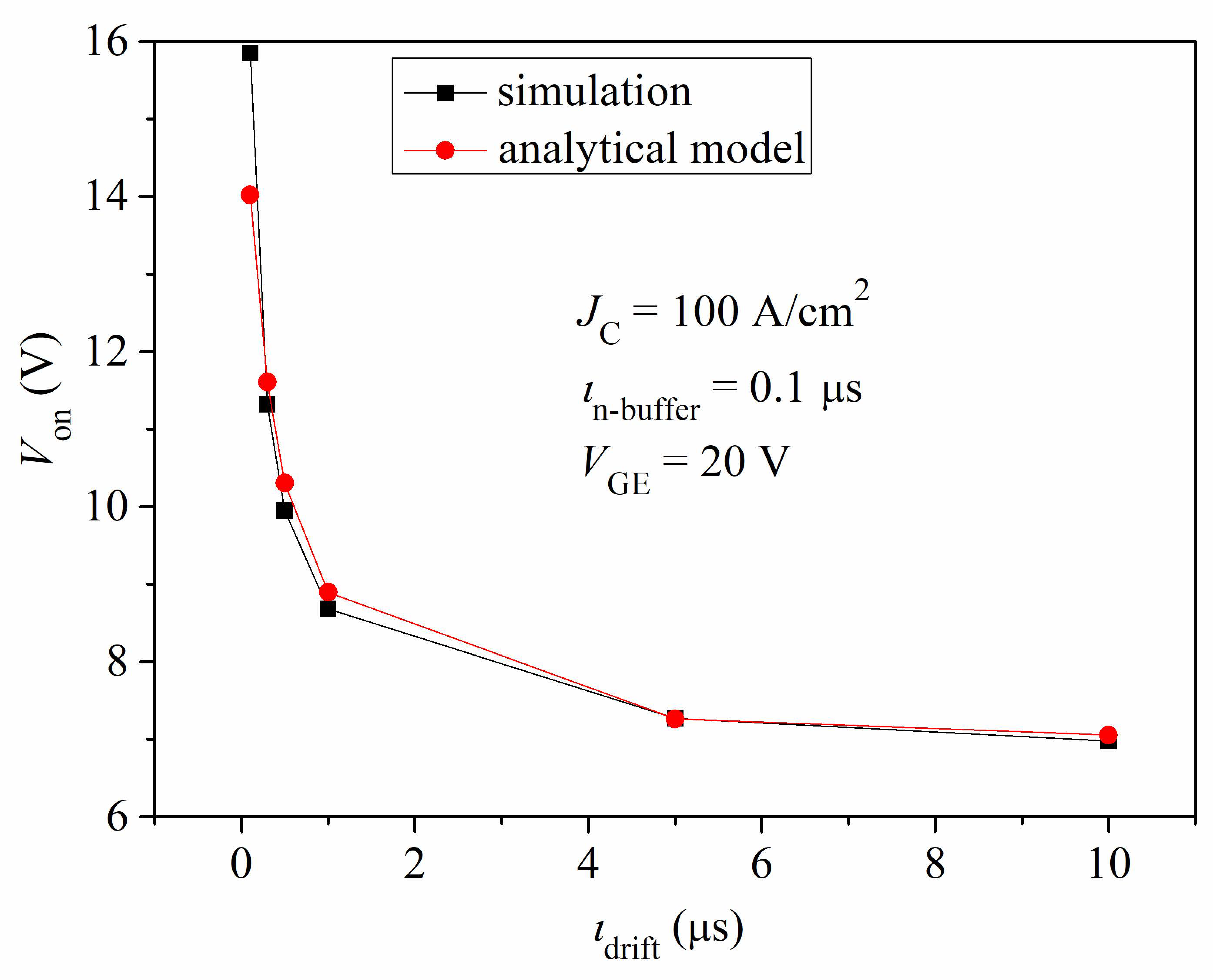
3. Simulation Results and Verification

This section describes the simulations carried out to investigate I-V characteristics and verify the forward voltage drop analytical model. The physical parameters of the investigated structure are given in Figure 1. In the simulation, the models utilized were as follows: the bandgap narrowing model (BGN); the AUGER and Shockley–Read–Hall (SRH) models for recombination and carrier lifetime; and doping and temperature-dependent field mobility models (ANALYTIC). Moreover, all the simulations were performed using Fermi–Dirac statistics. Selberherr’s impact ionization model was also utilized. In addition, it is worth noting that the simulator was calibrated to the experimental data of ref. [23]. Thus, in this paper, we adopted the same physical parameters as ref. [23]. Moreover, τn-buffer was set at 0.1 μs. The effect of τdrift is also discussed.
Figure 2 shows the transfer curve (at Vce = 4 V) and the I-V curve (at VGE = 20 V). From these graphs, it can be determined that Vth(on) is 5.8 V, and Von at JC = 100 A/cm2 is 8.68 V. The concentration distribution of the hole carriers at the buffer and drift regions is presented in Figure 3 and compared with analytic solutions obtained by the analytical model (Equation (9)). The analytical model can accurately describe the carrier’s concentration distribution, except for region A. The main reason may be explained as follows: Although the hole-carrier concentration is decaying in an exponential manner in both regions, Lp,BL is larger than that in the N-drift region. So, in the buffer layer, the minor carrier concentration decreases faster. However, in this paper, we assume that the hole-carrier concentration undergoes an exponential decay from junction J1 to J2, and La is the exponential decay index.
The influence of τdrift on Von is given in Figure 4, and is also compared with analytical values. From this figure, it can be seen that the simulation value coincides well with the analytical values at the higher carrier lifetime. The difference between the simulation and analytical values is larger at the lower carrier lifetime, because the built analytical model neglects the influence of carrier recombination occurring in the N-drift region. However, a recombination effect cannot be omitted when the carrier lifetime is lower, causing the appearance of the above-mentioned deviation.

4. Conclusions

A forward voltage drop analytical model was developed and investigated. The analytical model considered the hole-carrier concentration profile as a simple exponential form, in order to calculate the N-drift voltage more simply. A 2D numerical simulation was used to verify the correctness of the analytical model. The investigation results demonstrate that the developed model can exactly describe the distribution of the minor carrier concentration, and the analytical values agree well with the simulation results in quantity.

Author Contributions

Conceptualization, Y.L. and J.F.; methodology, Y.L.; software, Y.L., J.F. and D.J.; validation, Y.L. and D.J.; investigation, Y.L. and J.F.; writing—original draft preparation, Y.L.; writing—review and editing, Y.L., D.J. and J.F. All authors have read and agreed to the published version of the manuscript.

Funding

This research was funded by the Natural Science Foundation of Liaoning Province, grant number 2021-BS-192 and, in part, by the PhD research startup foundation of Shenyang Aerospace University, grant number 19YB47.

Institutional Review Board Statement

Not applicable.

Informed Consent Statement

Not applicable.

Data Availability Statement

Not applicable.

Conflicts of Interest

The authors declare no conflict of interest.

References

  1. Roccaforte, F.; Fiorenza, P.; Greco, G.; Nigro, R.L.; Giannazzoa, F.; Iucolanob, F.; Saggiob, M. Emerging Trends in Wide Band Gap Semiconductors (SiC and GaN) Technology for Power Devices. Microelectron. Eng. 2018, 187–188, 66–77. [Google Scholar] [CrossRef]
  2. Nawaz, M. Predicting Potential of 4H-SiC Power Devices Over 10 kV. In Proceedings of the 2013 IEEE 10th International Conference on Power Electronics and Drive Systems (PEDS), Kitakyushu, Japan, 22–25 April 2013; pp. 1291–1296. [Google Scholar]
  3. Kumar, V.; Verma, J.; Maan, A.S.; Akhtar, J. Epitaxial 4H-SiC based Schottky diode temperature sensors in ultra-low current range. Vacuum 2020, 182, 109590. [Google Scholar] [CrossRef]
  4. Kumar, V.; Maan, A.S.; Akhtar, J. Barrier height inhomogeneities induced anomaly in thermal sensitivity of Ni/4H-SiC Schottky diode temperature sensor. J. Vac. Sci. Technol. B 2014, 32, 041203. [Google Scholar] [CrossRef]
  5. Tang, G.; Tang, X.; Song, Q.; Yang, S.; Zhang, Y.; Zhang, Y.; Zhang, Y. Frequency-Improved 4H-SiC IGBT with Multizone Collector Design. IEEE Trans. Electron Devices 2020, 67, 198–203. [Google Scholar] [CrossRef]
  6. Wei, J.; Zhang, M.; Jiang, H.P.; Li, B.K.; Chen, K.J. Gate Structure Design of SiC Trench IGBTs for Injection-Enhancement Effect. IEEE Trans. Electron Devices 2019, 66, 3034–3039. [Google Scholar] [CrossRef]
  7. Wang, Y.; Yu, C.; Mao, H.; Wu, X.; Su, F.; Li, X.; Yang, J. Low Turn-Off Loss 4H-SiC Insulated Gate Bipolar Transistor with a Trench Heterojunction Collector. IEEE J. Electron Devices Soc. 2020, 8, 1010–1015. [Google Scholar] [CrossRef]
  8. Yang, T.; Wang, Y.; Yue, R. SiC Trench MOSFET with Reduced Switching Loss and Increased Short-Circuit Capability. IEEE Trans. Electron Devices 2020, 67, 3685–3690. [Google Scholar] [CrossRef]
  9. Wen, Z.-X.; Zhang, F.; Shen, Z.-W.; Chen, J.; He, Y.-W.; Yan, G.-G.; Liu, X.-F.; Zhao, W.-S.; Wang, L.; Sun, G.-S.; et al. Design and Fabrication of 10-kV Silicon-Carbide p-channel IGBTs with Hexagonal Cells and Step Space Modulated Junction Termination Extension. Chin. Phys. B 2019, 28, 068504. [Google Scholar] [CrossRef]
  10. Chowdhury, S.; Hitchcock, C.; Stum, Z. 4H-SiC n-Channel Insulated Gate Bipolar Transistors on (0001) and (000-1) Oriented Free-Standing n− Substrates. IEEE Electron Device Lett. 2016, 37, 317–320. [Google Scholar] [CrossRef]
  11. Ryu, S.; Capell, C.; Van Brunt, E. Ultra High Voltage MOS Controlled 4H-SiC Power Switching Devices. Semicond. Sci. Technol. 2015, 30, 084001. [Google Scholar] [CrossRef]
  12. Menon, K.G.; Nakajima, A.; Ngwendson, L. Performance Evaluation of 10-kV SiC Trench Clustered IGBT. IEEE Electron Device Lett. 2011, 32, 1272–1274. [Google Scholar]
  13. Menon, K.G.; Narayanan, E.M.S. Numerical Evaluation of 10-kV Clustered Insulated Gate Bipolar Transistor in 4H-SiC. IEEE Trans. Electron Devices 2013, 60, 366–373. [Google Scholar] [CrossRef]
  14. Lee, M.C.; Huang, A.Q. An Injection Efficiency Model to Characterize the Injection Capability and Turn-off Speed for >10 kV 4H-SiC IGBTs. Solid-State Electron. 2014, 93, 27–39. [Google Scholar] [CrossRef]
  15. Wang, H.Y.; Su, M.; Sheng, K. Theoretical Performance Limit of the IGBT. IEEE Trans. Electron Devices 2017, 64, 4148–4192. [Google Scholar]
  16. Hohannesson, D.; Nawaz, M.; Norrga, S.; Anders, H.; Nee, H.-P. Static and Dynamic Performance Prediction of Ultrahigh-Voltage Silicon Carbide Insulated-Gate Bipolar Transistors. IEEE Trans. Power Electron. 2021, 36, 5874–5891. [Google Scholar] [CrossRef]
  17. Liu, Y.; Wang, Y.; Yu, C.; Fei, C. 4H-SiC Trench IGBT with Lower On-State Voltage Drop. Superlattices Microstruct. 2017, 103, 53–63. [Google Scholar] [CrossRef] [Green Version]
  18. Liu, Y.-J.; Wang, Y.; Hao, Y.; Yu, C.-H.; Cao, F. 4H-SiC Trench IGBT with Back-Side n-p-n Collector for Low Turn-Off Loss. IEEE Trans. Electron Devices 2017, 64, 488–493. [Google Scholar] [CrossRef]
  19. Liu, Y.-J.; Wang, Y.; Hao, Y.; Fang, J.P.; Shan, C.; Cao, F. A Low Turn-Off Loss 4H-SiC Trench IGBT with Schottky Contact in the Collector Side. IEEE Trans. Electron Devices 2017, 64, 4575–4580. [Google Scholar] [CrossRef]
  20. Silvaco Int. Two Dimensional Device Simulation Program; Silvaco Int.: Santa Clara, CA, USA, 2012. [Google Scholar]
  21. Jayant Baliga, B. Silicon Carbide Power Devices, 3rd ed.; 5 Toh Tuck Link; World Scientific Publishing Co., Pte. Ltd.: Singapore, 2006; pp. 343–345. [Google Scholar]
  22. Jayant Baliga, B. Fundamentals of Power Semiconductor Devices, 3rd ed.; 5 Toh Tuck Link; World Scientific Publishing Co., Pte. Ltd.: Singapore, 2008; pp. 208–215. [Google Scholar]
  23. Usman, M.; Nawaz, M. Device design assessment of 4H–SiC n-IGBT—A simulation study. Solid-State Electron. 2014, 92, 5–11. [Google Scholar] [CrossRef]
Figure 1. Forward voltage drop distribution and hole concentration profile.
Crystals 12 00582 g001
Figure 2. Transfer and I–V characteristics.
Crystals 12 00582 g002
Figure 3. Hole-carrier concentration profile in buffer and drift regions.
Crystals 12 00582 g003
Figure 4. Influence of carrier lifetime in the drift region on forward voltage drop.
Crystals 12 00582 g004
Publisher’s Note: MDPI stays neutral with regard to jurisdictional claims in published maps and institutional affiliations.

