Abstract
GaN and NiO/GaN electrodes were characterized by impedance spectroscopy measurements in 0.1 M NaOH. We observed the suppression of the surface states capacitance due to the modification of the chemical state of superficial Ga atoms by NiO. This result suggests that the carriers involved in the photocorrosion of GaN in alkaline conditions originate in its surface states. In addition, we characterized the epitaxial relationship between the NiO particles deposited on GaN by transmission electron microscopy, finding the NiO||GaN and NiO ||GaN symmetry constraints.
1. Introduction
III-nitrides are of great interest in technological applications due to their optoelectronic properties. They are widely used in light-emitting diodes (LEDs) [1,2] and lately in micro-LEDs [3,4] because of the possibility of tuning their emission wavelength based on the metallic stoichiometry of their active region. In addition, they also have adequate band edges positions to drive water splitting [5] and artificial photosynthesis reactions [6,7,8,9,10,11], which is one of the most stringent requirements for photocatalysts of those reactions. However, their poor chemical endurance when used in photoelectrochemical (PEC) cells is one of their major flaws, especially in alkaline electrolytes [12,13].
The photocorrosion in n-GaN occurs by its oxidation into Ga3+ and N2 by the holes generated during the absorption of photons with energies larger than its band gap. Its mechanism still needs to be identified, although considering that catalysis is a surface-related phenomenon, electronic surface states should be involved in this process. The existence of surface states in GaN is well known. Their origin in Ga-polar GaN has been attributed either to dangling bonds of Ga atoms at the surface or to Ga adatoms bonded to three surface Ga atoms [14,15]. These states are responsible for the GaN Fermi level pinning by taking carriers from the space-charge region (SCR) near the GaN surface [16]. Under illumination, these states can trap the electrons generated in the SCR, which is detrimental for photocatalysts, although an oxidation treatment seems to passivate them partially [17]. Thus, surface states strongly affect the charge kinetics at the GaN/electrolyte interface, either in dark or illuminated conditions.
Metals and metal oxide (MO) cocatalysts, such as NiO, FeO, and CoO [18,19,20,21,22,23,24,25,26,27,28,29,30,31], have proven to be helpful to increase the chemical endurance of nitrides and their PEC activity. Still, the mechanism of these improvements has not been established. The role of cocatalysts is usually depicted as an aide to decrease the overpotential necessary to drive the chemical reaction of interest, affecting the kinetics of the reaction solely. MOs are well-known catalyst and cocatalyst materials, particularly useful in the oxidation-side reactions, such as the oxygen evolution reaction in water splitting. The mechanism of this reaction is commonly described as either a charge transfer promoted in the surface metal-sites or involving the reversible formation of lattice-oxygen into a superficial oxygen vacancy [32,33,34,35]. In the case of MO/GaN photoelectrodes, there is evidence suggesting that the MO does not participate directly in the chemical reaction. For example, if GaN is covered even by a few nm thin film of MO, its PEC activity is almost null [26], implying that the chemical reaction occurs not in the MO but in the GaN region. In such a case, GaN would not only work as the photoabsorber, but its surface would act as the catalytic region, with the MOs improving only the charge kinetics between GaN and the electrolyte.
Previous studies of NiO as a GaN cocatalyst [36,37] have overlooked its effect on the surface states of GaN and focused on the modification of its surface band structure. However, the performance of NiO/GaN photoelectrodes showed no clear correlation with their flat band potential. In this work, we analyzed the electrical properties of different GaN photoelectrodes decorated with NiO particles using electrochemical impedance spectroscopy (EIS). We analyzed the effect of NiO in the SCR capacitance of electrodes and the impedance related to the surface states. In addition, we present the observation and crystalline properties of NiO particles deposited on GaN and describe the epitaxial relationship found between both materials.
2. Materials and Methods
Four GaN electrodes were prepared for analysis by EIS. The GaN structure was grown by metalorganic vapor phase epitaxy on a c-plane patterned sapphire substrate (PSS). The pattern pitch, diameter, and height of the sapphire substrate were 3.0, 2.6, and 1.6 μm, respectively. The epi-structure consisted of (top to bottom) unintentionally doped (uid)-GaN (100 nm)/n-GaN (3 μm, Si-doped, n = 3 × 1018 cm−3)/uid-GaN (2 μm). We used a PSS to improve the crystalline quality of GaN [38,39]. The purpose of the bottom uid-GaN layer was to avoid the carrier trapping by defects, given its low electrical conductivity. In contrast, the n-GaN layer provides an appropriate electrical path for electron extraction. Finally, the top uid-GaN layer extends the surface depletion region to a thickness comparable to the light penetration depth of GaN, improving the photoabsorption capabilities of the electrode [40].
Three of the four electrodes were decorated with NiO particles by spin coating using different diluted NiO metalorganic decomposition (MOD) solutions, following a method similar to the one described elsewhere [26] but with varying dilution ratios. The three solutions were prepared using 2, 4, and 10 μL of MOD diluted in 1.05 mL of butyl acetate and 450 μL of 1 M NaOH (the electrodes prepared with each one of the solutions will be referred to henceforth as 2 μL NiO/GaN, 4 μL NiO/GaN, and 10 μL NiO/GaN). All the electrodes were annealed in air at 500 °C for 30 min, including the bare GaN electrode. After the annealing, a copper wire was soldered onto the surface of the electrodes using indium to form an ohmic contact, and the metallic regions on the surface of the electrodes were electrically isolated by covering them with epoxy resin. The coverage of the GaN surface by the NiO particles was investigated using scanning electron microscopy (SEM). To study the crystalline properties of the NiO deposited on GaN, a cross-sectional lamella was prepared by focused ion beam from the 10 μL NiO/GaN sample, which was analyzed afterward by transmission electron microscopy (TEM). Additionally, X-ray photoelectron spectroscopy (XPS) was used to characterize the chemical state of the surface atoms of the electrodes.
The single-sine EIS analyses were conducted in 0.1 M NaOH under dark conditions, using a three-electrode configuration with different DC biases. The AC signal had an amplitude of 10 mV, and its frequency varied from 5 Hz to 50 kHz. Two-electrode measurements were performed to evaluate the PEC performance of the electrodes. In those measurements, a platinum wire was used as the counter electrode, and the GaN electrodes were irradiated with a power density of 100 mWcm−2 using a 300 W Xe arc lamp with an ultraviolet (UV) spectroscopic mirror.
3. Results and Discussion
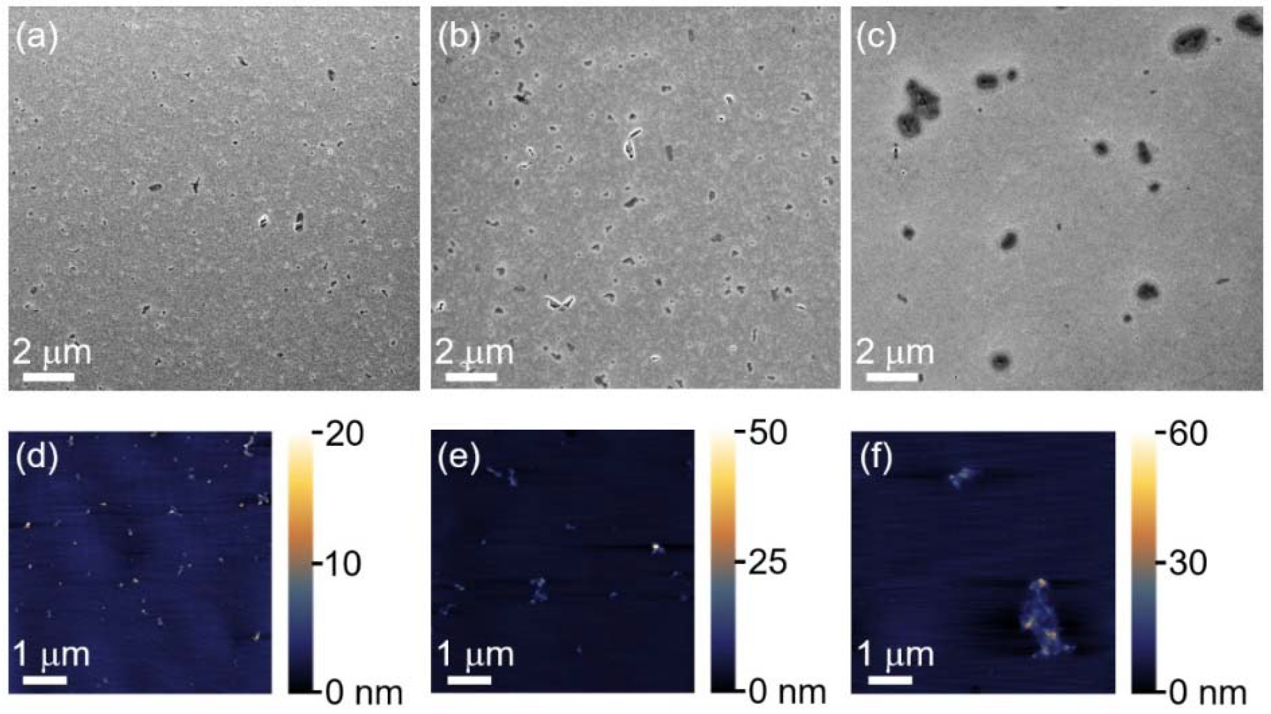
After the deposition of the NiO particles, the surface of the electrodes was studied by SEM and atomic force microscopy (AFM). Figure 1a–c shows the surface of the NiO/GaN electrodes, where the NiO particles appeared as dark spots. The coverage of the GaN surface by the NiO particles was 0.5% for the 2 μL NiO/GaN, 1.2% for the 4 μL NiO/GaN, and 1.8% for the 10 μL NiO/GaN. The AFM analyses show different aggregation topographies, with the thicknesses of the particles ranging from a few nm up to a few tens of nanometers in some regions.
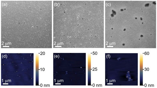
Figure 1.
(Top) SEM and (bottom) AFM images of the (a,d) 2 μL NiO/GaN, (b,e) 4 μL NiO/GaN, and (c,f) 10 μL NiO/GaN photoelectrodes surfaces. The black regions in the SEM micrographs correspond to the NiO particles deposited.
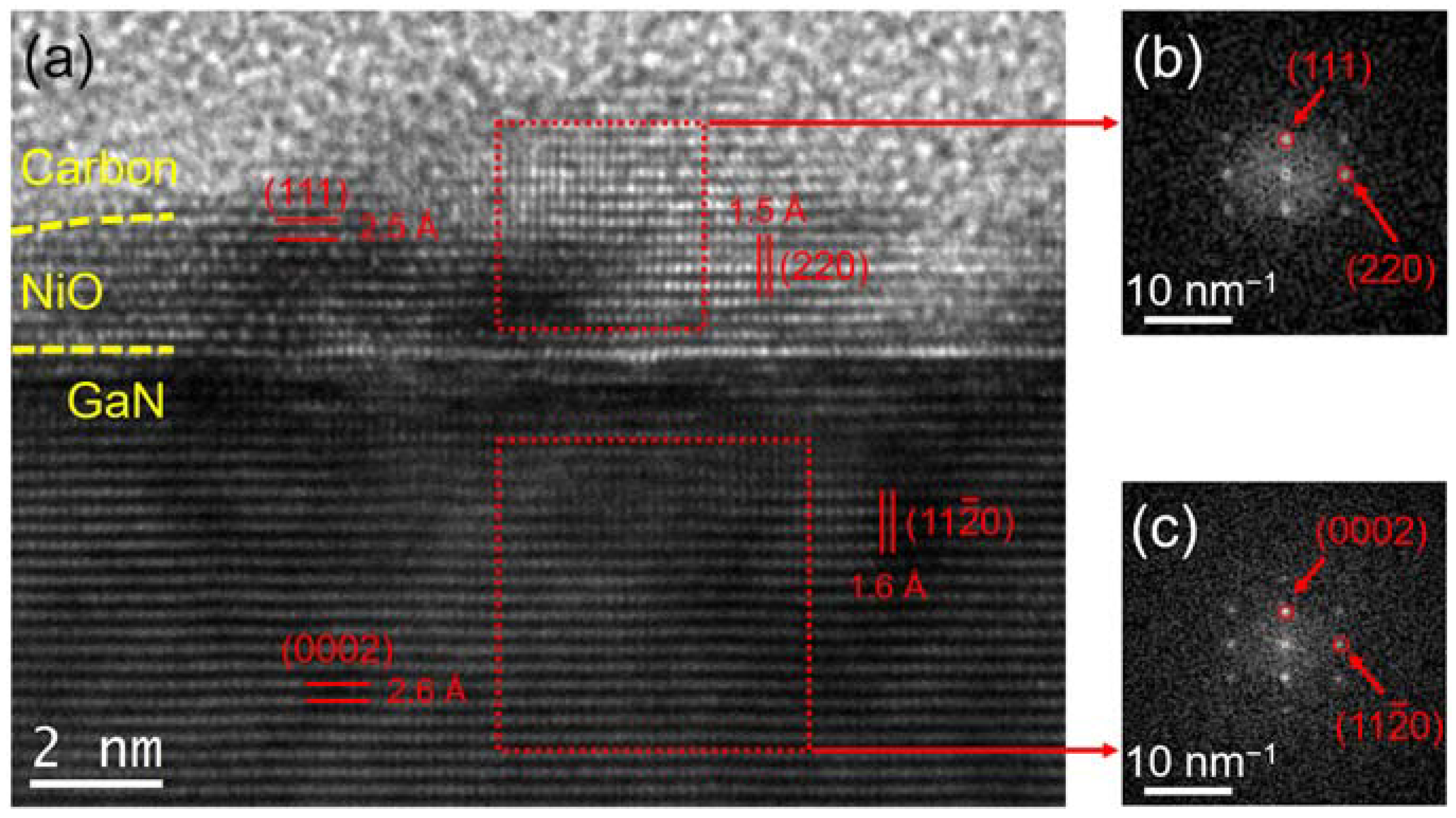
The crystalline characterization of the NiO deposited on GaN showed an epitaxial relationship between these materials. Figure 2a shows a high-resolution TEM micrograph of the NiO/GaN interface, where some lattice spacings are marked based on the numerical diffractograms obtained from each region. It is observed that the epitaxial relation exhibited the NiO||GaN and NiO||GaN symmetry constraints, which are equivalent to others previously reported [41,42]. The epitaxial relation between these materials arises from the geometrical symmetries and size of their crystalline structure. Regardless of NiO having a cubic crystalline structure (a = 0.4195 nm), NiO planes have hexagonal symmetry, which corresponds to the symmetry of the GaN planes. In addition, the in-plane symmetry is favored due to the low mechanical strain generated by a minor lattice-spacing mismatch of only 7% between the NiO and GaN planes.
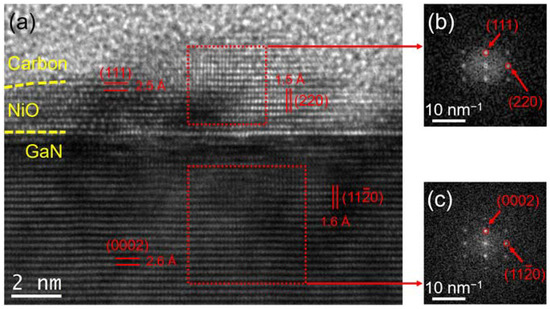
Figure 2.
(a) High-resolution TEM micrograph at the NiO/GaN interface. (b,c) show the numerical diffractograms of NiO and GaN, respectively, from the regions enclosed in the squares in (a). The TEM lamella was prepared from the 10 μL NiO/GaN sample.
Figure 3 shows the current response of the electrodes during constant irradiation in a two-electrode configuration. The current of the bare GaN electrode suffers a quick degradation due to the expected photocorrosion. However, in all the decorated electrodes, the photocurrent keeps a stable behavior, with a slight rise over time.
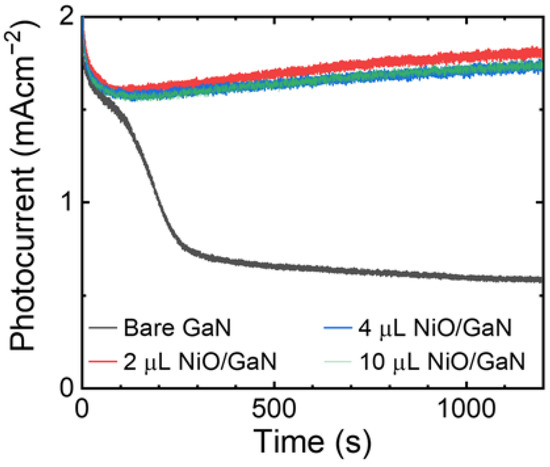
Figure 3.
Photocurrent response of the bare GaN and NiO/GaN electrodes at zero bias. The irradiation power was 100 mWcm−2 using 0.1 M NaOH as an electrolyte.
In the EIS measurements, the bulk capacitance Cbulk of the electrodes was found after fitting their impedance by an equivalent circuit (EC) model. However, Cbulk is not only composed of the SCR capacitance CSC, as it usually also contains the contribution from the Helmholtz capacitance CH formed at the semiconductor/electrolyte interface. In most cases, such contribution can be neglected because CH >> CSC and, given that both capacitances are in series, Cbulk ≈ CSC [43]. The behavior of CSC as a function of the applied voltage is described by the Mott-Schottky equation:
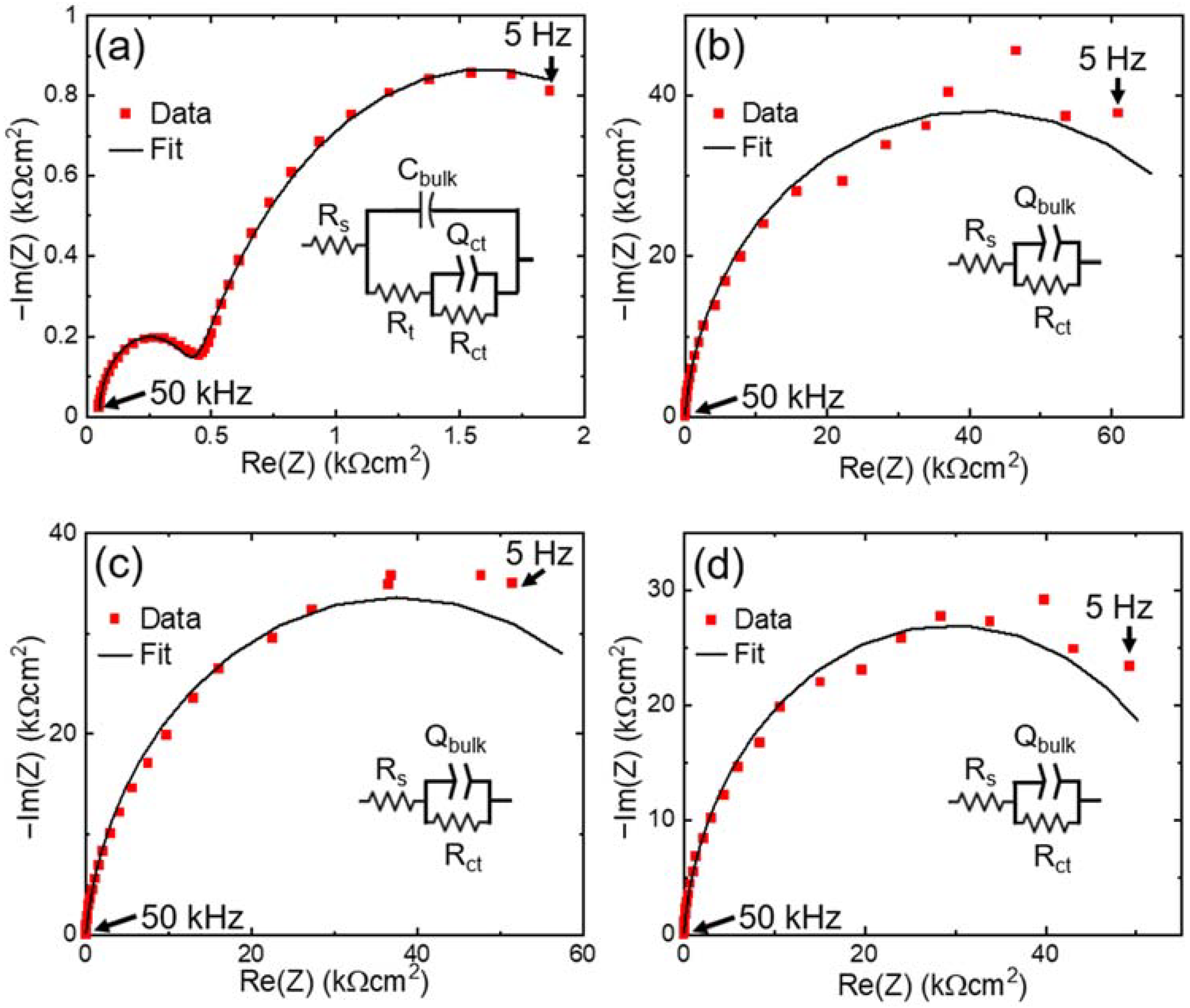
where is the electrode area, is the elementary charge, is the dielectric constant of the semiconductor, is the vacuum permittivity, is the donor density, is the flat band potential, and the temperature. Figure 4 shows the typical Nyquist plots for the bare and NiO/GaN electrodes. The bare GaN results exhibited two time constants, but only one dominant time constant was present in the NiO/GaN electrodes. The EC elements chosen to fit the impedance of the electrodes were selected based on the processes of displacement/accumulation of carriers expected to occur. The EC used to fit the behavior of each electrode is shown as an inset in the corresponding graph of Figure 4.
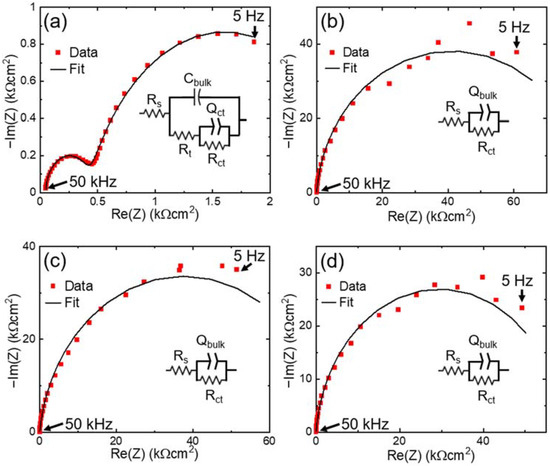
Figure 4.
The real and imaginary parts of the impedance Z of the (a) bare GaN, (b) 2 μL NiO/GaN, (c) 4 μL NiO/GaN, and (d) 10 μL NiO/GaN electrodes. The scattered data correspond to the experimental data, and the solid black lines are the fits obtained using the circuit shown as an inset in each graph. The electrodes were immersed in 0.1 M NaOH, and their potential was −1.1 V vs. Ag/AgCl/KCl (sat.). The data points were obtained by sweeping the frequency from 5 Hz to 50 kHz. The points corresponding to 5 Hz and 50 kHz are indicated.
The observation of two time constants in the bare GaN electrode is attributed to the bulk capacitance and the distribution of surface states [44]. The EC used to model this behavior was composed of a series resistance Rs related to the contact resistance of the electrode, a capacitor corresponding to the bulk capacitance of the semiconductor, and an impedance part associated with the trapping of carriers by surface states. The trapping was described by a resistance Rt in series with a resistance and capacitor in parallel. The capacitance of the trapping state was modeled using a constant phase element (CPE) Qct rather than a capacitor due to its higher accuracy to emulate non-ideal capacitors. The impedance of this CPE is given by , where and are frequency-independent parameters characteristic of Qct. A pseudocapacitance can be extracted from the values of Qct and Rct, which is given by
Analogously, a pseudocapacitance value Cbulk can be extracted from Qbulk and Rct in the case of the NiO/GaN electrodes.
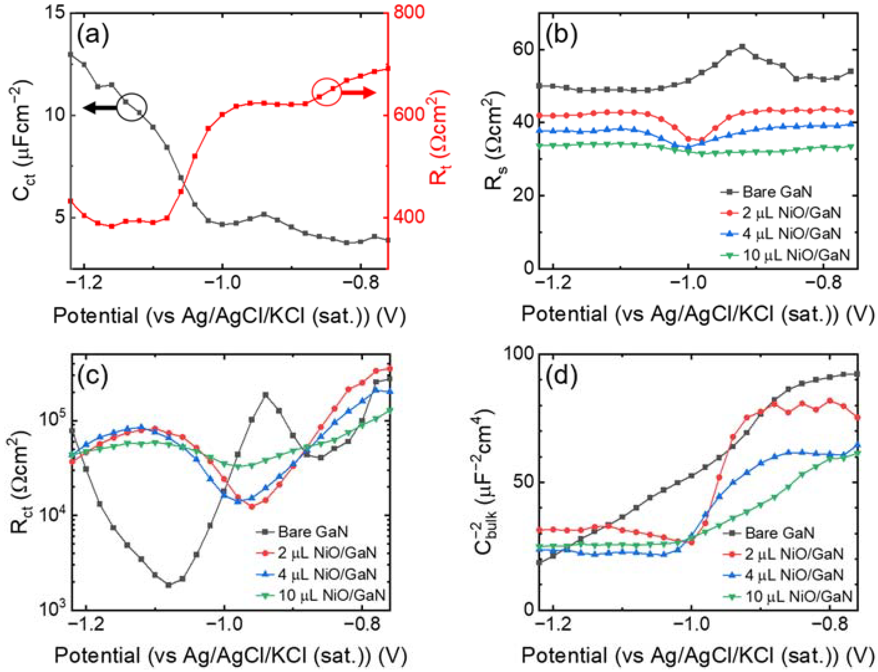
Figure 5 shows the capacitance and resistance values found from the ECs fittings as a function of the electrode potential. Figure 5a shows that the increase in the trapping capacitance Cct of the bare GaN electrode seems to be correlated to the decrease in Rt, showing the influence of the surface states in the kinetics of electrons from the conduction band. Figure 5b shows small variations of Rs as a function of the applied voltage to the electrode and had a value of a few tens of Ω·cm2, which is the expected behavior of the contact resistance. The behavior of Rct is quite different in the bare GaN electrode than in the NiO/GaN electrodes, as shown in Figure 5c. When Rct reaches a local maximum in the bare GaN electrode, Rct in the NiO/GaN electrodes is around a local minimum. There is a maximum in Rct for the bare GaN electrode at −0.94 V vs. Ag/AgCl/KCl (sat.), which corresponds to a local maximum in Cct. It is expected that the surface state capacitance traces a peak with respect to the Fermi level variation, in this case, controlled by the electrode voltage, at the point where the Fermi level is equal to the energy level of the surface state [45]. Therefore, these results suggest that in the bare GaN electrode, the energy level of the surface states is at around 0.94 eV vs. Ag/AgCl/KCl (sat.) (in 0.1 M NaOH). However, there might be some correction considering the kinetics of the carriers when there is illumination.
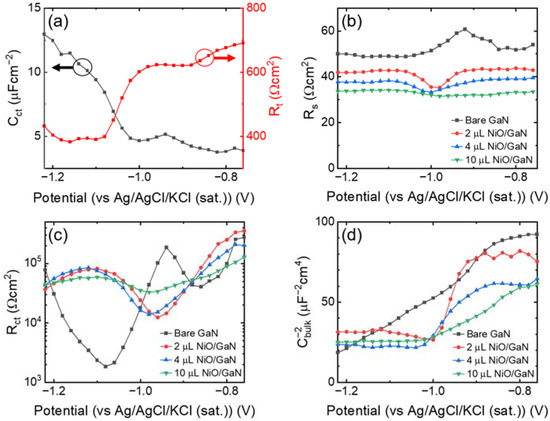
Figure 5.
(a) Cct and Rt corresponding to the equivalent circuit of the bare GaN electrode shown as an inset in Figure 4a. (b–d) Rs, Rct, and Cbulk of the bare GaN and NiO/GaN electrodes fabricated in this work. Cbulk is presented in its usual form related to Equation (1). The measurements were performed in 0.1 M NaOH.
One of the significant differences in the characterization of the electrodes fabricated is that the NiO decorated electrodes can be modeled without the surface state capacitance. Previous works have shown that the photocorrosion potential of GaN in acidic media corresponds to the energy level of the surface states [17]. Although the photocorrosion mechanism in alkaline conditions may vary from that in acidic media, the photocorrosion suppression when the surface states of GaN are passivated suggests that a similar photocorrosion mechanism also happens in alkaline conditions. Figure 5d shows Cbulk of the GaN electrodes. Following Equation (1), the shift between the different traces of Cbulk means that different flat band potential values are expected for each one of the electrodes. However, the PEC performance of the NiO/GaN electrodes was practically the same, as shown by Figure 3. The marginal difference shown by the 2 μL NiO/GaN electrode likely originated from its slightly better photoabsorption due to a lower surface coverage by NiO. This result also shows that any modification to the bulk band structure parameters by NiO did not significantly affect the overall performance of the electrodes.
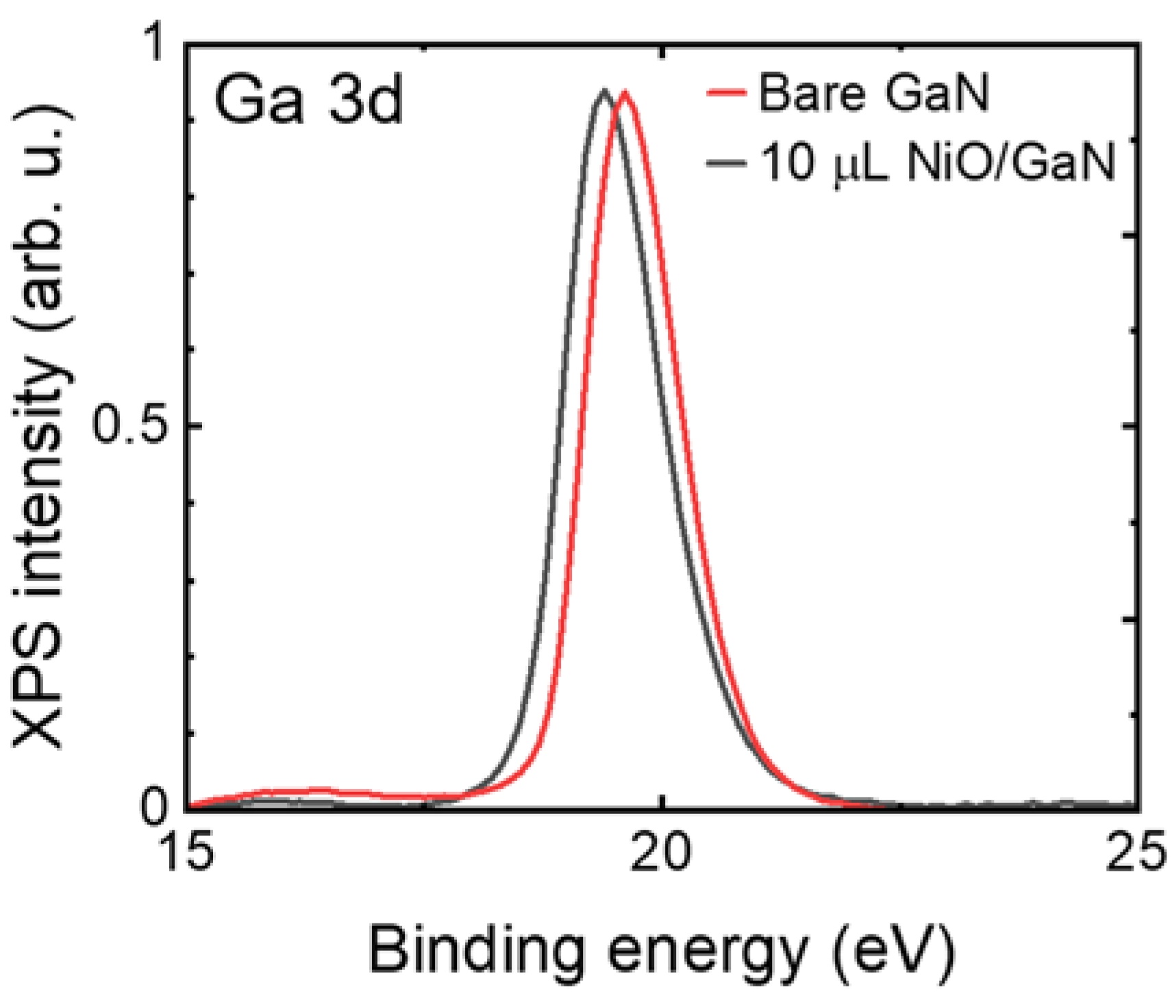
Given that the origin of the surface states is either the dangling bonds from the surface Ga atoms or Ga adatoms bonded to them, the passivation should occur by modifying the chemical bindings of those superficial atoms. XPS analyses were performed to confirm if there were any differences in the chemical state between the Ga atoms of the bare GaN and 10 μL NiO/GaN electrodes. The results of this measurement are shown in Figure 6. With the introduction of the NiO cocatalyst, the binding peak shifted 0.2 eV in the negative direction. The Ga 3d peak position is well known to be influenced by the chemical bonding of Ga atoms [46]. Therefore, we can conclude that in the case of NiO deposited on the bulk GaN, the two materials formed a chemical bonding with the participation of surface Ga atoms, passivating the surface states this way. Other works report similar photocorrosion suppression techniques where surface termination species are added [47]. However, in the case of NiO deposited on GaN, the coverage necessary to prevent photocorrosion is negligible, which lets the semiconductor preserve almost intact its photoabsorption properties.

Figure 6.
Ga 3d peaks of the X-ray photoelectron spectroscopy measurements obtained from the bare GaN and 10 μL NiO/GaN electrodes. The peak of the bare GaN electrode is shifted 0.2 eV towards a higher binding energy with respect to the NiO decorated electrode.
4. Conclusions
In conclusion, we characterized the surface states in GaN by EIS analyses and demonstrated that NiO particles deposited directly on GaN passivate them. These surface states are generated by the electronic bindings of superficial Ga atoms, and the interaction of those atoms with NiO modifies its chemical structure, as demonstrated by XPS measurements. Finally, TEM analyses demonstrated that the NiO deposited as a cocatalyst preserved an epitaxial relationship with GaN, following the NiO||GaN and NiO||GaN symmetry constraints.
Author Contributions
Conceptualization, M.V.-R. and K.O.; methodology, M.V.-R., P.K. and D.I.; validation, Z.Z., D.I. and M.V.-R.; formal analysis, Z.Z. and D.I.; investigation, M.V.-R.; resources, M.V.-R., Z.Z. and D.I.; data curation, M.V.-R. and P.K.; writing—original draft preparation, M.V.-R.; writing—review and editing, Z.Z., D.I. and K.O.; supervision, K.O.; funding acquisition, K.O. All authors have read and agreed to the published version of the manuscript.
Funding
King Abdullah University of Science and Technology (BAS/1/1676-01-01).
Data Availability Statement
Data underlying the results presented in this paper are not publicly available but may be obtained from the authors upon reasonable request.
Conflicts of Interest
The authors declare no conflict of interest.
References
- Barletta, P.T.; Berkman, E.A.; Moody, B.F.; El-Masry, N.A.; Emara, A.M.; Reed, M.J.; Bedair, S.M. Development of Green, Yellow, and Amber Light Emitting Diodes Using InGaN Multiple Quantum Well Structures. Appl. Phys. Lett. 2007, 90, 151109. [Google Scholar] [CrossRef]
- Ohkawa, K.; Watanabe, T.; Sakamoto, M.; Hirako, A.; Deura, M. 740-Nm Emission from InGaN-Based LEDs on c-Plane Sapphire Substrates by MOVPE. J. Cryst. Growth 2012, 343, 13–16. [Google Scholar] [CrossRef]
- Zhuang, Z.; Iida, D.; Ohkawa, K. Ultrasmall and Ultradense InGaN-Based RGB Monochromatic Micro-Light-Emitting Diode Arrays by Pixilation of Conductive p-GaN. Photonics Res. 2021, 9, 2429. [Google Scholar] [CrossRef]
- Zhuang, Z.; Iida, D.; Velazquez-Rizo, M.; Ohkawa, K. 630-Nm Red InGaN Micro-Light-Emitting Diodes (<20 Μm × 20 Μm) Exceeding 1 MW/Mm 2 for Full-Color Micro-Displays. Photonics Res. 2021, 9, 1796. [Google Scholar] [CrossRef]
- Fujii, K.; Karasawa, T.; Ohkawa, K. Hydrogen Gas Generation by Splitting Aqueous Water Using N-Type GaN Photoelectrode with Anodic Oxidation. Jpn. J. Appl. Phys. Part 2 Lett. 2005, 44, 543–545. [Google Scholar] [CrossRef]
- Brunner, D.; Angerer, H.; Bustarret, E.; Freudenberg, F.; Höpler, R.; Dimitrov, R.; Ambacher, O.; Stutzmann, M. Optical Constants of Epitaxial AlGaN Films and Their Temperature Dependence. J. Appl. Phys. 1997, 82, 5090–5096. [Google Scholar] [CrossRef]
- Chichibu, S.F.; Hazu, K.; Ishikawa, Y.; Tashiro, M.; Ohtomo, T.; Furusawa, K.; Uedono, A.; Mita, S.; Xie, J.; Collazo, R.; et al. Excitonic Emission Dynamics in Homoepitaxial AlN Films Studied Using Polarized and Spatio-Time-Resolved Cathodoluminescence Measurements. Appl. Phys. Lett. 2013, 103, 142103. [Google Scholar] [CrossRef]
- Araki, T.; Saito, Y.; Yamaguchi, T.; Kurouchi, M.; Nanishi, Y.; Naol, H. Radio Frequency-Molecular Beam Epitaxial Growth of InN Epitaxial Films on (0001) Sapphire and Their Properties. J. Vac. Sci. Technol. B Microelectron. Nanometer Struct. 2004, 22, 2139–2143. [Google Scholar] [CrossRef]
- Vurgaftman, I.; Meyer, J.R. Band Parameters for Nitrogen-Containing Semiconductors. J. Appl. Phys. 2003, 94, 3675–3696. [Google Scholar] [CrossRef]
- Moses, P.G.; Miao, M.; Yan, Q.; Van De Walle, C.G. Hybrid Functional Investigations of Band Gaps and Band Alignments for AlN, GaN, InN, and InGaN. J. Chem. Phys. 2011, 134, 084703. [Google Scholar] [CrossRef]
- Moses, P.G.; Van De Walle, C.G. Band Bowing and Band Alignment in InGaN Alloys. Appl. Phys. Lett. 2010, 96, 2–5. [Google Scholar] [CrossRef]
- Minsky, M.S.; White, M.; Hu, E.L. Room-Temperature Photoenhanced Wet Etching of GaN. Appl. Phys. Lett. 1996, 68, 1531–1533. [Google Scholar] [CrossRef]
- Youtsey, C.; Adesida, I.; Bulman, G. Highly Anisotropic Photoenhanced Wet Etching of N-Type GaN. Appl. Phys. Lett. 1997, 71, 2151–2153. [Google Scholar] [CrossRef]
- Wang, F.H.; Krüger, P.; Pollmann, J. Electronic Structure of 1 × 1 GaN(0001) and GaN(0001) Surfaces. Phys. Rev. B-Condens. Matter Mater. Phys. 2001, 64, 0353051–0353058. [Google Scholar] [CrossRef]
- van de Walle, C.G.; Segev, D. Microscopic Origins of Surface States on Nitride Surfaces. J. Appl. Phys. 2007, 101, 81704. [Google Scholar] [CrossRef] [Green Version]
- Segev, D.; van de Walle, C.G. Origins of Fermi-Level Pinning on GaN and InN Polar and Nonpolar Surfaces. Europhys. Lett. 2006, 76, 305–311. [Google Scholar] [CrossRef]
- Baker, D.R.; Lundgren, C.A. Electrochemical Determination of the Gallium-Nitride Photocorrosion Potential in Acidic Media. J. Mater. Chem. A 2017, 5, 20978–20984. [Google Scholar] [CrossRef]
- Fujii, K.; Ono, M.; Ito, T.; Iwaki, Y.; Hirako, A.; Ohkawa, K. Band-Edge Energies and Photoelectrochemical Properties of n-Type AlxGa1−x N and InyGa1−y N Alloys. J. Electrochem. Soc. 2007, 154, B175. [Google Scholar] [CrossRef]
- Ono, M.; Fujii, K.; Ito, T.; Iwaki, Y.; Hirako, A.; Yao, T.; Ohkawa, K. Photoelectrochemical Reaction and H2 Generation at Zero Bias Optimized by Carrier Concentration of n-Type GaN. J. Chem. Phys. 2007, 126, 054708. [Google Scholar] [CrossRef]
- Hayashi, T.; Deura, M.; Ohkawa, K. High Stability and Efficiency of GaN Photocatalyst for Hydrogen Generation from Water. Jpn. J. Appl. Phys. 2012, 51, 50–52. [Google Scholar] [CrossRef]
- Ohkawa, K.; Ohara, W.; Uchida, D.; Deura, M. Highly Stable GaN Photocatalyst for Producing H2 Gas from Water. Jpn. J. Appl. Phys. 2013, 52, 2–4. [Google Scholar] [CrossRef]
- Yotsuhashi, S.; Deguchi, M.; Zenitani, Y.; Hinogami, R.; Hashiba, H.; Yamada, Y.; Ohkawa, K. Photo-Induced CO2 Reduction with GaN Electrode in Aqueous System. Appl. Phys. Express 2011, 4, 2–4. [Google Scholar] [CrossRef]
- Yotsuhashi, S.; Deguchi, M.; Hashiba, H.; Zenitani, Y.; Hinogami, R.; Yamada, Y.; Ohkawa, K. Enhanced CO2 Reduction Capability in an AlGaN/GaN Photoelectrode. Appl. Phys. Lett. 2012, 100, 2010–2013. [Google Scholar] [CrossRef]
- Hashiba, H.; Yotsuhashi, S.; Deguchi, M.; Yamada, Y.; Ohkawa, K. Selectivity Control of CO2 Reduction in an Inorganic Artificial Photosynthesis System. Appl. Phys. Express 2013, 6, 2–5. [Google Scholar] [CrossRef]
- Sekimoto, T.; Hashiba, H.; Shinagawa, S.; Uetake, Y.; Deguchi, M.; Yotsuhashi, S.; Ohkawa, K. Analysis of Products from Photoelectrochemical Reduction of 13CO2 by GaN-Si Based Tandem Photoelectrode. J. Phys. Chem. C 2016, 120, 13970–13975. [Google Scholar] [CrossRef]
- Velazquez-Rizo, M.; Iida, D.; Ohkawa, K. Photoelectrochemical and Crystalline Properties of a GaN Photoelectrode Loaded with α-Fe2O3 as Cocatalyst. Sci. Rep. 2020, 10, 12586. [Google Scholar] [CrossRef]
- Velazquez-Rizo, M.; Iida, D.; Ohkawa, K. Photoelectrochemical H 2 Generation from Water Using a CoO x /GaN Photoelectrode. Japanese J. Appl. Phys. 2019, 58, SCCC23. [Google Scholar] [CrossRef]
- Alqahtani, M.; Sathasivam, S.; Alhassan, A.; Cui, F.; Benjaber, S.; Blackman, C.; Zhang, B.; Qin, Y.; Parkin, I.P.; Nakamura, S.; et al. InGaN/GaN Multiple Quantum Well Photoanode Modified with Cobalt Oxide for Water Oxidation. ACS Appl. Energy Mater. 2018, 1, 6417–6424. [Google Scholar] [CrossRef]
- Maeda, K.; Teramura, K.; Saito, N.; Inoue, Y.; Domen, K. Photocatalytic Overall Water Splitting on Gallium Nitride Powder. Bull. Chem. Soc. Jpn. 2007, 80, 1004–1010. [Google Scholar] [CrossRef]
- Hou, Y.; Syed, Z.A.; Smith, R.; Athanasiou, M.; Gong, Y.; Yu, X.; Bai, J.; Wang, T. Enhanced Water Splitting with Silver Decorated GaN Photoelectrode. J. Phys. D Appl. Phys. 2016, 49, 265601. [Google Scholar] [CrossRef]
- Yoshida, M.; Yamakata, A.; Takanabe, K.; Kubota, J.; Osawa, M.; Domen, K. ATR-SEIRAS Investigation of the Fermi Level of Pt Cocatalyst on a GaN Photocatalyst for Hydrogen Evolution under Irradiation. J. Am. Chem. Soc. 2009, 131, 13218–13219. [Google Scholar] [CrossRef]
- Grimaud, A.; Diaz-Morales, O.; Han, B.; Hong, W.T.; Lee, Y.L.; Giordano, L.; Stoerzinger, K.A.; Koper, M.T.M.; Shao-Horn, Y. Activating Lattice Oxygen Redox Reactions in Metal Oxides to Catalyse Oxygen Evolution. Nat. Chem. 2017, 9, 457–465. [Google Scholar] [CrossRef]
- Yoo, J.S.; Rong, X.; Liu, Y.; Kolpak, A.M. Role of Lattice Oxygen Participation in Understanding Trends in the Oxygen Evolution Reaction on Perovskites. ACS Catal. 2018, 8, 4628–4636. [Google Scholar] [CrossRef]
- Nørskov, J.K.; Rossmeisl, J.; Logadottir, A.; Lindqvist, L.; Kitchin, J.R.; Bligaard, T.; Jónsson, H. Origin of the Overpotential for Oxygen Reduction at a Fuel-Cell Cathode. J. Phys. Chem. B 2004, 108, 17886–17892. [Google Scholar] [CrossRef]
- Koper, M.T.M. Theory of Multiple Proton-Electron Transfer Reactions and Its Implications for Electrocatalysis. Chem. Sci. 2013, 4, 2710–2723. [Google Scholar] [CrossRef] [Green Version]
- Koike, K.; Yamamoto, K.; Ohara, S.; Sugiyama, M.; Nakano, Y.; Fujii, K. Photoelectrochemical Property Differences between NiO Dots and Layer on N-Type GaN for Water Splitting. J. Electrochem. Soc. 2016, 163, H1091–H1095. [Google Scholar] [CrossRef]
- Koike, K.; Yamamoto, K.; Ohara, S.; Kikitsu, T.; Ozasa, K.; Nakamura, S.; Sugiyama, M.; Nakano, Y.; Fujii, K. Effects of NiO-Loading on n-Type GaN Photoanode for Photoelectrochemical Water Splitting Using Different Aqueous Electrolytes. Int. J. Hydrogen Energy 2017, 42, 9493–9499. [Google Scholar] [CrossRef]
- Song, J.C.; Lee, S.H.; Lee, I.H.; Seol, K.W.; Kannappan, S.; Lee, C.R. Characteristics Comparison between GaN Epilayers Grown on Patterned and Unpatterned Sapphire Substrate (0 0 0 1). J. Cryst. Growth 2007, 308, 321–324. [Google Scholar] [CrossRef]
- Zhou, S.; Yuan, S.; Liu, Y.; Guo, L.J.; Liu, S.; Ding, H. Highly Efficient and Reliable High Power LEDs with Patterned Sapphire Substrate and Strip-Shaped Distributed Current Blocking Layer. Appl. Surf. Sci. 2015, 355, 1013–1019. [Google Scholar] [CrossRef]
- Iwaki, Y.; Ono, M.; Yamaguchi, K.; Kusakabe, K.; Fujii, K.; Ohkawa, K. Nitride Photocatalyst to Generate Hydrogen Gas from Water. Phys. Status Solidi (C) Curr. Top. Solid State Phys. 2008, 5, 2349–2351. [Google Scholar] [CrossRef]
- Roccaforte, F.; Greco, G.; Fiorenza, P.; Raineri, V.; Malandrino, G.; Lo Nigro, R. Epitaxial NiO Gate Dielectric on AlGaN/GaN Heterostructures. Appl. Phys. Lett. 2012, 100, 63511. [Google Scholar] [CrossRef]
- Baraik, K.; Singh, S.D.; Kumar, Y.; Ajimsha, R.S.; Misra, P.; Jha, S.N.; Ganguli, T. Epitaxial Growth and Band Alignment Properties of NiO/GaN Heterojunction for Light Emitting Diode Applications. Appl. Phys. Lett. 2017, 110, 191603. [Google Scholar] [CrossRef]
- Hankin, A.; Bedoya-Lora, F.E.; Alexander, J.C.; Regoutz, A.; Kelsall, G.H. Flat Band Potential Determination: Avoiding the Pitfalls. J. Mater. Chem. A 2019, 7, 26162–26176. [Google Scholar] [CrossRef] [Green Version]
- Kocha, S.S.; Peterson, M.W.; Arent, D.J.; Redwing, J.M.; Tischler, M.A.; Turner, J.A. Electrochemical Investigation of the Gallium Nitride-Aqueous Electrolyte Interface. J. Electrochem. Soc. 1995, 142, L238–L240. [Google Scholar] [CrossRef]
- Klahr, B.; Gimenez, S.; Fabregat-Santiago, F.; Hamann, T.; Bisquert, J. Water Oxidation at Hematite Photoelectrodes: The Role of Surface States. J. Am. Chem. Soc. 2012, 134, 4294–4302. [Google Scholar] [CrossRef] [Green Version]
- Nefedov, V.I.; Salyn, Y.v.; Domashevskaya, E.P.; Ugai, Y.A.; Terekhov, V.A. A Study by XPS and XRS of the Participation in Chemical Bonding of the 3d Electrons of Copper, Zinc and Gallium. J. Electron Spectrosc. Relat. Phenom. 1975, 6, 231–238. [Google Scholar] [CrossRef]
- Hu, S.; Shaner, M.R.; Beardslee, J.A.; Lichterman, M.; Brunschwig, B.S.; Lewis, N.S. Amorphous TiO2 Coatings Stabilize Si, GaAs, and GaP Photoanodes for Efficient Water Oxidation. Science 2014, 344, 1005–1009. [Google Scholar] [CrossRef] [Green Version]

Publisher’s Note: MDPI stays neutral with regard to jurisdictional claims in published maps and institutional affiliations. |
© 2022 by the authors. Licensee MDPI, Basel, Switzerland. This article is an open access article distributed under the terms and conditions of the Creative Commons Attribution (CC BY) license (https://creativecommons.org/licenses/by/4.0/).