
Morphology Transition of Te-Doped InAs Nanowire on InP(111)B Grown Using MOCVD Method

 , ,
, , 
Abstract
1. Introduction
2. Materials and Methods
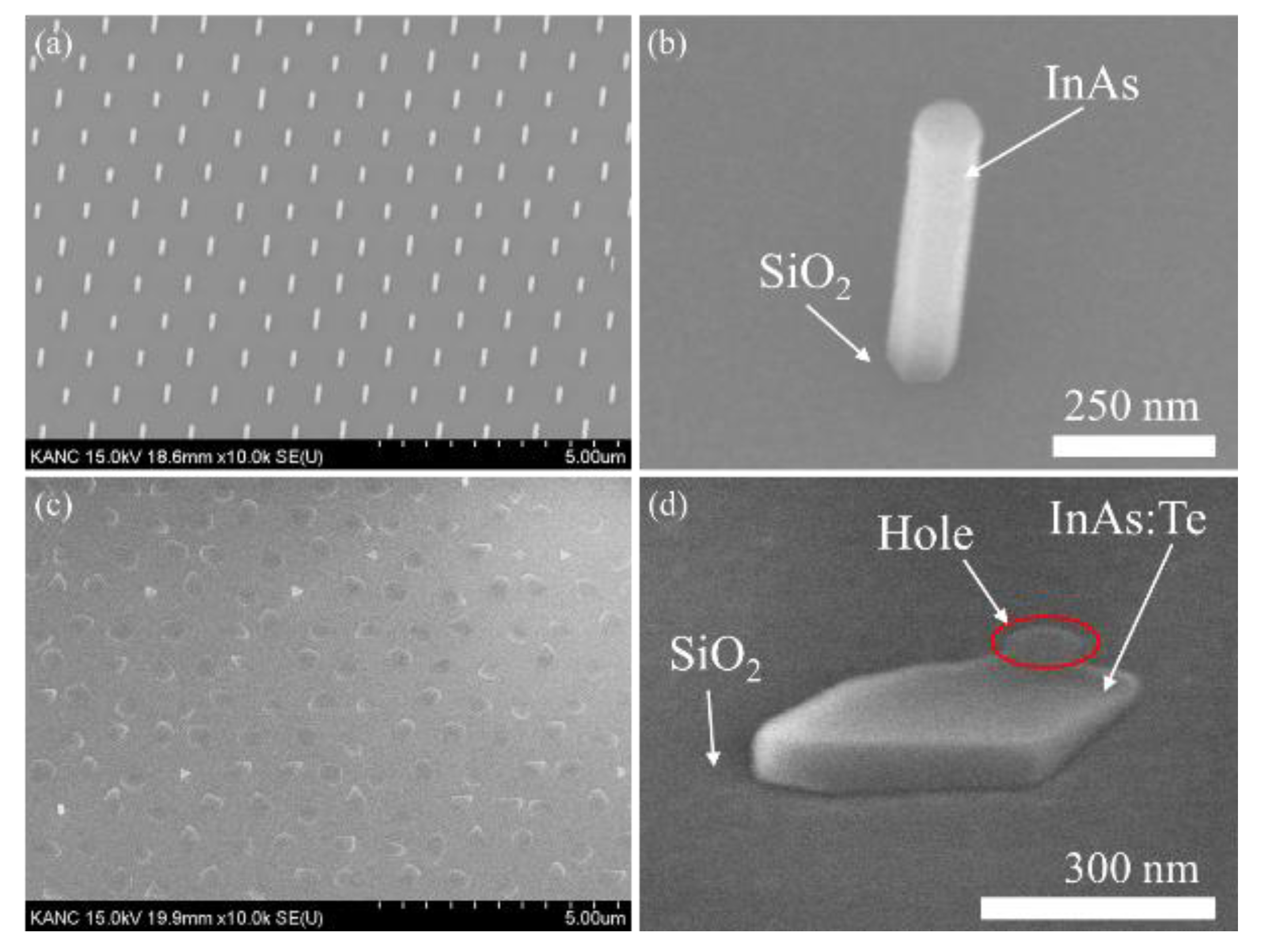
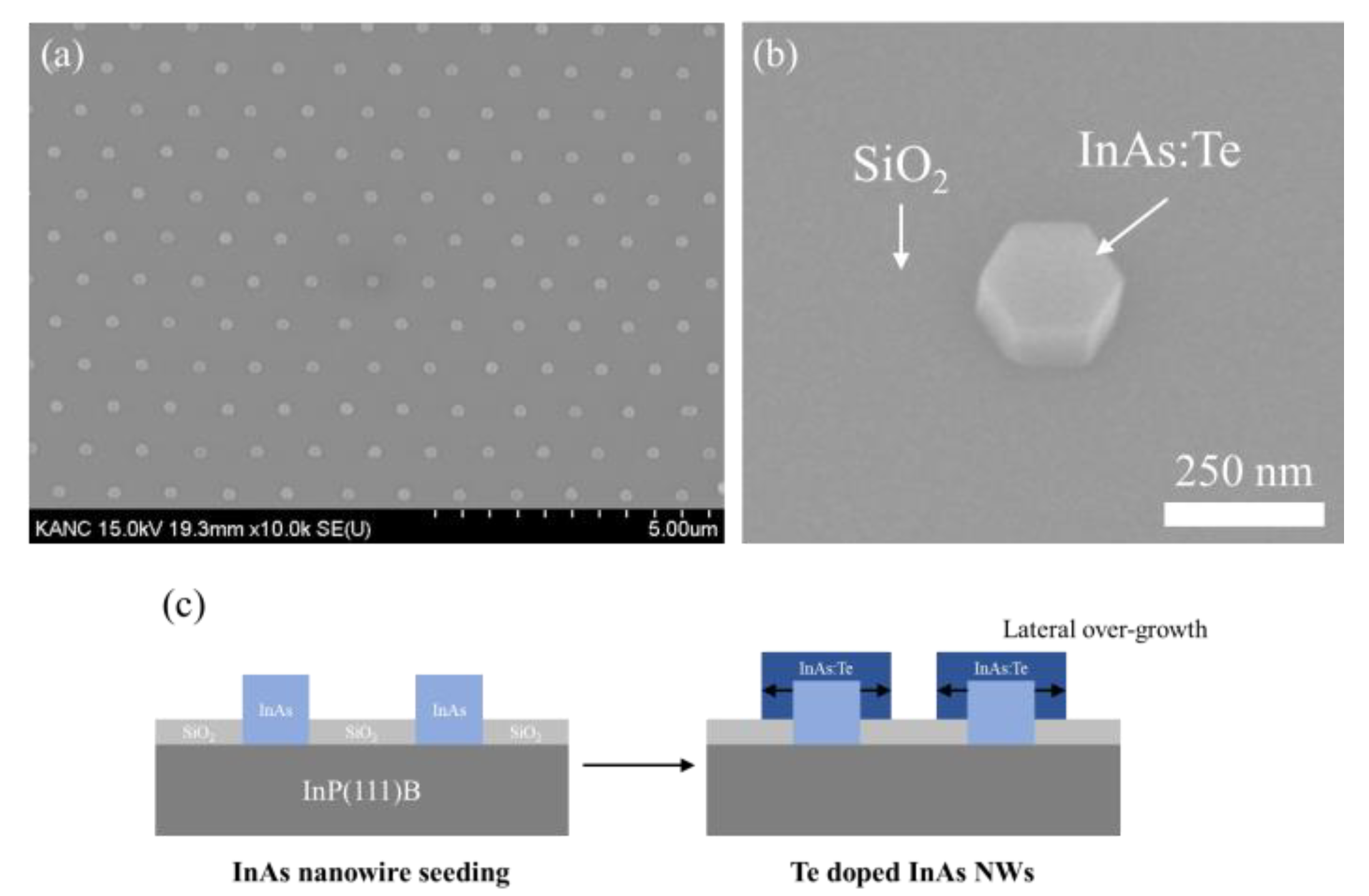
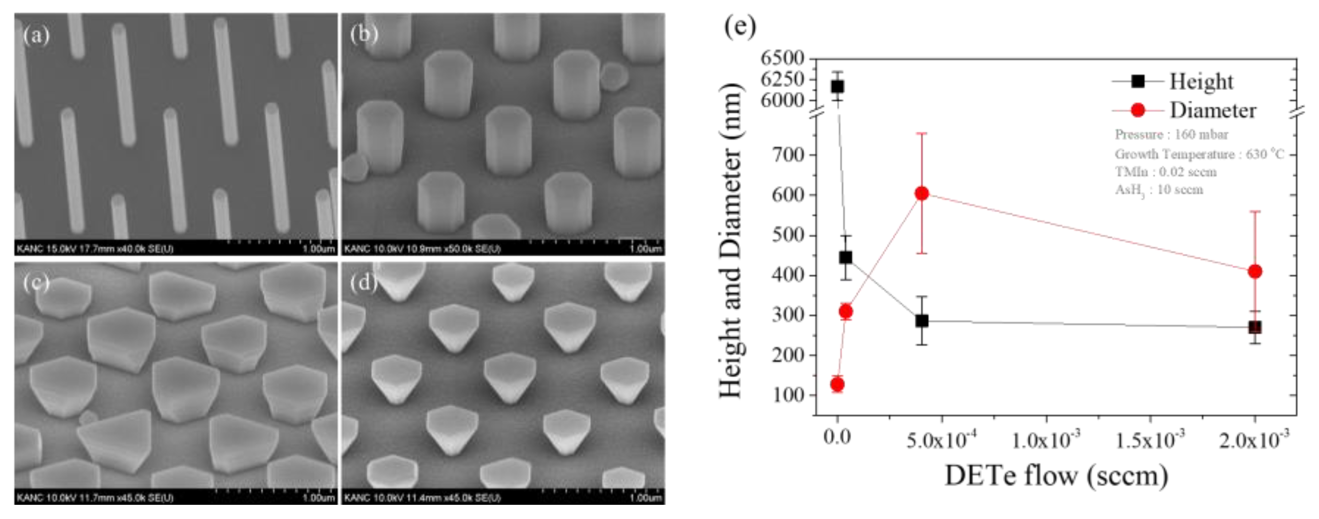
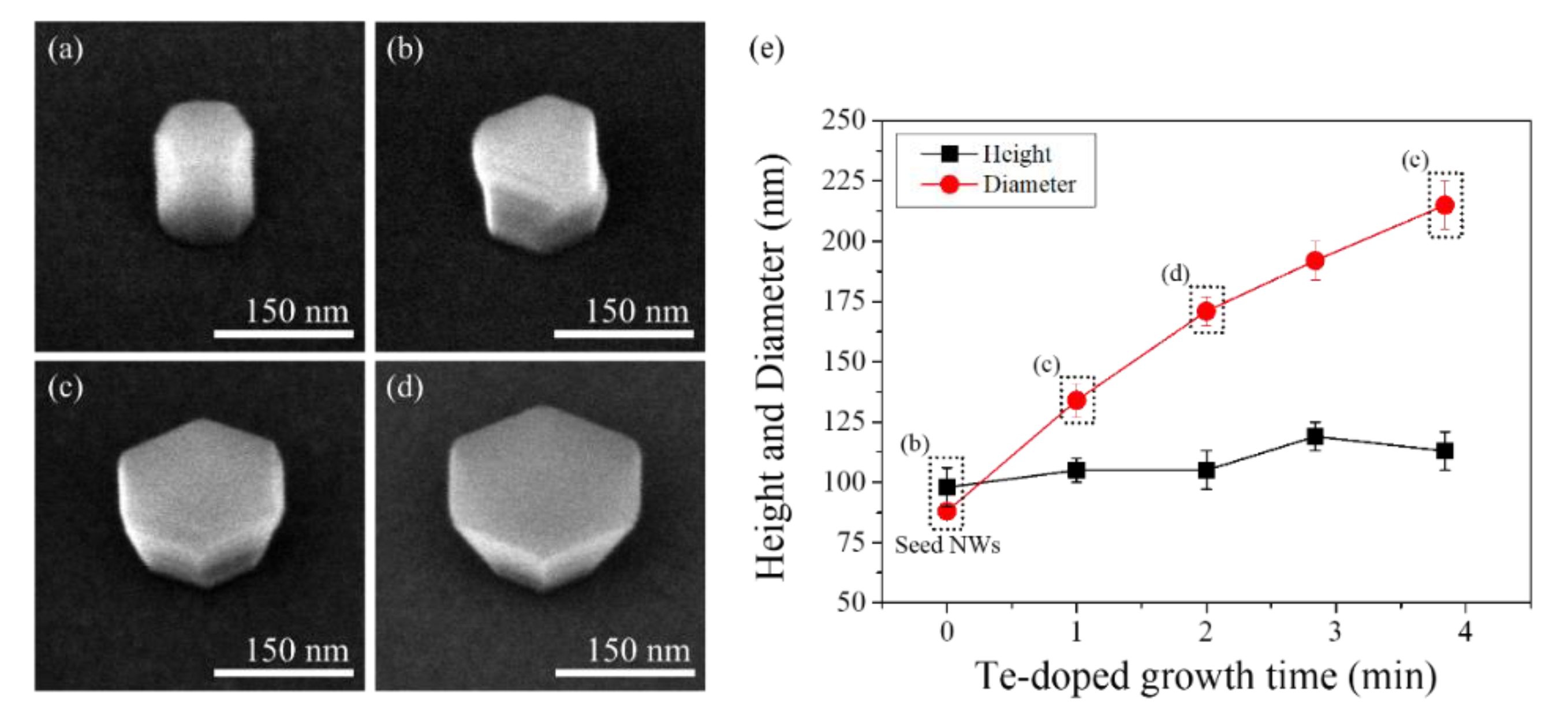
3. Results and Discussion
4. Conclusions
Author Contributions
Funding
Institutional Review Board Statement
Informed Consent Statement
Data Availability Statement
Conflicts of Interest
References
- Khanal, D.R.; Wu, J. Gate coupling and charge distribution in nanowire field effect transistors. Nano Lett. 2007, 7, 2778–2783. [Google Scholar] [CrossRef]
- Breuer, S.; Pfüller, C.; Flissikowski, T.; Brandt, O.; Grahn, H.T.; Geelhaar, L.; Riechert, H. Suitability of au- and self-assisted GaAs nanowires for optoelectronic applications. Nano Lett. 2011, 11, 1276–1279. [Google Scholar] [CrossRef] [PubMed]
- Jiang, Z.; Qing, Q.; Xie, P.; Gao, R.; Lieber, C.M. Kinked p-n junction nanowire probes for high spatial resolution sensing and intracellular recording. Nano Lett. 2012, 12, 1711–1716. [Google Scholar] [CrossRef] [PubMed]
- Wallentin, J.; Anttu, N.; Asoli, D.; Huffman, M.; Åberg, I.; Magnusson, M.H.; Siefer, G.; Fuss-Kailuweit, P.; Dimroth, F.; Witzigmann, B.; et al. InP Nanowire Array Solar Cells Achieving 13.8% Efficiency by Exceeding the Ray Optics Limit. Science 2013, 339, 1057–1060. [Google Scholar] [CrossRef] [PubMed]
- Dai, X.; Zhang, S.; Wang, Z.; Adamo, G.; Liu, H.; Huang, Y.; Couteau, C.; Soci, C. GaAs/AlGaAs nanowire photodetector. Nano Lett. 2014, 14, 2688–2693. [Google Scholar] [CrossRef]
- Guo, W.; Zhang, M.; Banerjee, A.; Bhattacharya, P. Catalyst-free InGaN/GaN nanowire light emitting diodes grown on (001) silicon by molecular beam epitaxy. Nano Lett. 2010, 10, 3355–3359. [Google Scholar] [CrossRef]
- Konar, A.; Mathew, J.; Nayak, K.; Bajaj, M.; Pandey, R.K.; Dhara, S.; Murali, K.V.R.M.; Deshmukh, M.M. Carrier transport in high mobility InAs nanowire junctionless transistors. Nano Lett. 2015, 15, 1684–1690. [Google Scholar] [CrossRef]
- Güsken, N.A.; Rieger, T.; Mussler, G.; Lepsa, M.I.; Grützmacher, D. Influence of Te-doping on catalyst-free VS InAs nanowires. Nanoscale Res. Lett. 2019, 14, 179. [Google Scholar] [CrossRef]
- Lubow, A.; Ismail-Beigi, S.; Ma, T. Comparison of drive currents in metal-oxide-semiconductor field-effect transistors made of Si, Ge, GaAs, InGaAs, And InAs channels. Appl. Phys. Lett. 2010, 96, 122105. [Google Scholar] [CrossRef]
- Takagi, S.; Zhang, R.; Suh, J.; Kim, S.; Yokoyama, M.; Nishi, K.; Takenaka, M. III–V/Ge Channel MOS Device Technologies in Nano CMOS Era. Jpn. J. Appl. Phys. 2015, 54, 06FA01. [Google Scholar] [CrossRef]
- del Alamo, J. Nanometre-Scale Electronics With III–V Compound Semiconductors. Nature 2011, 479, 317–323. [Google Scholar] [CrossRef]
- Morral, A. Gold-free GaAs nanowire synthesis and optical properties. IEEE J. Sel. Top. Quantum Electron. 2011, 17, 819–828. [Google Scholar] [CrossRef]
- Koblmüller, G.; Abstreiter, G. Growth and properties of InGaAs nanowires on silicon. Phys. Status Solidi RRL 2014, 8, 11–30. [Google Scholar] [CrossRef]
- Dong, R.; Yang, W.; Wu, P.; Hussain, M.; Xiu, Z.; Wu, G.; Wang, P. Microstructure characterization of SiC nanowires as reinforcements in composites. Mater. Charact. 2015, 103, 37–41. [Google Scholar] [CrossRef]
- Utama, M.I.B.; de la Mata, M.; Magen, C.; Arbiol, J.; Xiong, Q. Twinning-, Polytypism-, and Polarity-Induced Morphological Modulation in Nonplanar Nanostructures with van Der Waals Epitaxy. Adv. Funct. Mater. 2013, 23, 1636–1646. [Google Scholar] [CrossRef]
- Galvão Tizei, L.H.; Amato, M. Electronic Structure and Optical Properties of Semiconductor Nanowires Polytypes. Eur. Phys. J. B 2020, 93, 16. [Google Scholar] [CrossRef]
- Thelander, C.; Caroff, P.; Plissard, S.; Dey, A.W.; Dick, K.A. Effects of Crystal Phase Mixing on the Electrical Properties of InAs Nanowires. Nano Lett. 2011, 11, 2424–2429. [Google Scholar] [CrossRef]
- Schroer, M.D.; Petta, J.R. Correlating the Nanostructure and Electronic Properties of InAs Nanowires. Nano Lett. 2010, 10, 1618–1622. [Google Scholar] [CrossRef]
- Heiss, M.; Conesa-Boj, S.; Ren, J.; Tseng, H.-H.; Gali, A.; Rudolph, A.; Uccelli, E.; Peiró, F.; Morante, J.R.; Schuh, D.; et al. Direct Correlation of Crystal Structure and Optical Properties in Wurtzite/Zinc-Blende GaAs Nanowire Heterostructures. Phys. Rev. B Condens. Matter Mater. Phys. 2011, 83, 045303. [Google Scholar] [CrossRef]
- Schmid, H.; Moselund, K.E.; Bjork, M.T.; Richter, M.; Ghoneim, H.; Bessire, C.D.; Riel, H. Fabrication of Vertical InAs-Si Heterojunction Tunnel Field Effect Transistors. In Proceedings of the 69th Device Research Conference, Santa Barbara, CA, USA, 20–22 June 2011; IEEE: Piscataway, NJ, USA, 2011. [Google Scholar]
- Björk, M.T.; Knoch, J.; Schmid, H.; Riel, H.; Riess, W. Silicon Nanowire Tunneling Field-Effect Transistors. Appl. Phys. Lett. 2008, 92, 193504. [Google Scholar] [CrossRef]
- Suomalainen, S.; Hakkarainen, T.V.; Salminen, T.; Koskinen, R.; Honkanen, M.; Luna, E.; Guina, M. Te-Doping of Self-Catalyzed GaAs Nanowires. Appl. Phys. Lett. 2015, 107, 012101. [Google Scholar] [CrossRef]
- De-Sheng, J.; Makita, Y.; Ploog, K.; Queisser, H.J. Electrical Properties and Photoluminescence of Te-doped GaAs Grown by Molecular Beam Epitaxy. J. Appl. Phys. 1982, 53, 999–1006. [Google Scholar] [CrossRef]
- Grundmann, M. The Physics of Semiconductors: An Introduction Including Devices and Nanophysics, 1st ed.; Springer: Berlin, Germany, 2010. [Google Scholar]
- Ahmad, E.; Kasanaboina, P.K.; Karim, M.R.; Sharma, M.; Reynolds, C.L.; Liu, Y.; Iyer, S. Te Incorporation in GaAs1−xSbxnanowires and P-i-n Axial Structure. Semicond. Sci. Technol. 2016, 31, 125001. [Google Scholar] [CrossRef]
- Kennon, E.L.; Orzali, T.; Xin, Y.; Vert, A.; Lind, A.G.; Jones, K.S. Deactivation of Electrically Supersaturated Te-Doped InGaAs Grown by MOCVD. J. Mater. Sci. 2017, 52, 10879–10885. [Google Scholar] [CrossRef]
- LaPierre, R.R.; Chia, A.C.E.; Gibson, S.J.; Haapamaki, C.M.; Boulanger, J.; Yee, R.; Kuyanov, P.; Zhang, J.; Tajik, N.; Jewll, N.; et al. III–V nanowire photovoltaics: Review of design for high efficiency. Phys. Status Solidi RRL 2013, 7, 815–830. [Google Scholar] [CrossRef]
- Dimakis, E.; Ramsteiner, M.; Huang, C.-N.; Trampert, A.; Davydok, A.; Biermanns, A.; Pietsch, U.; Riechert, H.; Geelhaar, L. In Situ Doping of Catalyst-Free InAs Nanowires with Si: Growth, Polytypism, and Local Vibrational Modes of Si. Appl. Phys. Lett. 2013, 103, 143121. [Google Scholar] [CrossRef]
- Wirths, S.; Weis, K.; Winden, A.; Sladek, K.; Volk, C.; Alagha, S.; Weirich, T.E.; von der Ahe, M.; Hardtdegen, H.; Lüth, H.; et al. Effect of Si-Doping on InAs Nanowire Transport and Morphology. J. Appl. Phys. 2011, 110, 053709. [Google Scholar] [CrossRef]
- Wixom, R.R.; Rieth, L.W.; Stringfellow, G.B. Te Surfactant Effects on the Morphology of Patterned (001) GaAs Homoepitaxy. J. Cryst. Growth 2004, 269, 276–283. [Google Scholar] [CrossRef]
- Paquette, B.; Ilahi, B.; Aimez, V.; Arès, R. Inhibition of Te Surfactant Effect on Surface Morphology of Heavily Te-Doped GaAs. J. Cryst. Growth 2013, 383, 30–35. [Google Scholar] [CrossRef]
- Anyebe, E.A.; Rajpalke, M.K.; Veal, T.D.; Jin, C.J.; Wang, Z.M.; Zhuang, Q.D. Surfactant Effect of Antimony Addition to the Morphology of Self-Catalyzed InAs1−xSbx Nanowires. Nano Res. 2015, 8, 1309–1319. [Google Scholar] [CrossRef]
- Caroff, P.; Bolinsson, J.; Johansson, J. Crystal Phases in III--V Nanowires: From Random toward Engineered Polytypism. IEEE J. Sel. Top. Quantum Electron. 2011, 17, 829–846. [Google Scholar] [CrossRef]
- Harris, J.S., Jr.; Yuen, H.; Bank, S.; Wistey, M.; Lordi, V.; Gugov, T.; Bae, H.; Goddard, L. MBE Growth and Characterization of Long Wavelength Dilute Nitride III–V Alloys. In Dilute Nitride Semiconductors; Elsevier: Amsterdam, The Netherlands, 2005; pp. 1–92. [Google Scholar] [CrossRef]
- Jacobsson, D.; Panciera, F.; Tersoff, J.; Reuter, M.C.; Lehmann, S.; Hofmann, S.; Dick, K.A.; Ross, F.M. Interface Dynamics and Crystal Phase Switching in GaAs Nanowires. Nature 2016, 531, 317–322. [Google Scholar] [CrossRef]
- Guniat, L.; Caroff, P.; Fontcuberta i Morral, A. Vapor Phase Growth of Semiconductor Nanowires: Key Developments and Open Questions. Chem. Rev. 2019, 119, 8958–8971. [Google Scholar] [CrossRef]
- Tomioka, K.; Mohan, P.; Noborisaka, J.; Hara, S.; Motohisa, J.; Fukui, T. Growth of Highly Uniform InAs Nanowire Arrays by Selective-Area MOVPE. J. Cryst. Growth 2007, 298, 644–647. [Google Scholar] [CrossRef]
- Kodaira, R.; Hara, S.; Kabamoto, K.; Fujimagari, H. Synthesis and Structural Characterization of Vertical Ferromagnetic MnAs/Semiconducting InAs Heterojunction Nanowires. Jpn. J. Appl. Phys. 2016, 55, 075503. [Google Scholar] [CrossRef]
- Hertenberger, S.; Rudolph, D.; Bichler, M.; Finley, J.J.; Abstreiter, G.; Koblmüller, G. Growth kinetics in position-controlled and catalyst-free InAs nanowire arrays on Si(111) grown by selective area molecular beam epitaxy. J. Appl. Phys. 2010, 108, 114316. [Google Scholar] [CrossRef]
- Fathi Aghdam, F.; Liao, H.; Huang, Q. Modeling Interaction in Nanowire Growth Process Toward Improved Yield. IEEE Trans. Autom. Sci. Eng. 2017, 14, 1139–1149. [Google Scholar] [CrossRef]
- Hara, S.; Elm, M.T.; Klar, P.J. Selective-Area Growth and Transport Properties of MnAs/InAs Heterojunction Nanowires. J. Mater. Res. 2019, 34, 3863–3876. [Google Scholar] [CrossRef]
- Wang, X.; Bai, X.; Yang, X.; Liu, X.; Du, W.; Yang, T. A Theoretical and Experimental Study on Effect of Growth Time on Self-Catalyzed InAs Nanowires. Appl. Surf. Sci. 2020, 518, 146174. [Google Scholar] [CrossRef]
- Song, C.-H.; Kong, M.; Jang, H.; Tae Lee, S.; Park, H.-H.; Zoo Kim, C.; Hyun Jung, S.; Choi, Y.; Kim, S.; Ko, D.-H.; et al. Vertical Growth Characterization of InAs Nanowires Grown by Selective Area Growth on Patterned InP(1 1 1)B Substrate by a MOCVD Method. Solid State Electron. 2021, 175, 107939. [Google Scholar] [CrossRef]
- Lewis, R.B.; Corfdir, P.; Herranz, J.; Küpers, H.; Jahn, U.; Brandt, O.; Geelhaar, L. Self-Assembly of InAs Nanostructures on the Sidewalls of GaAs Nanowires Directed by a Bi Surfactant. Nano Lett. 2017, 17, 4255–4260. [Google Scholar] [CrossRef] [PubMed]
- Massies, J.; Grandjean, N. Surfactant Effect on the Surface Diffusion Length in Epitaxial Growth. Phys. Rev. B Condens. Matter. 1993, 48, 8502–8505. [Google Scholar] [CrossRef] [PubMed]
- Jeong, I.-Y.; Choi, M.; Kim, J.; Kim, Y.H.; Shin, J.C.; Kim, E.K.; Kim, C.-S.; Song, S. Mixed Phase Confirmation of InAsxP1−x Nanowire Array Using Modified Reciprocal Space Mapping. Electron. Mater. Lett. 2022, 18, 79–86. [Google Scholar] [CrossRef]


Publisher’s Note: MDPI stays neutral with regard to jurisdictional claims in published maps and institutional affiliations. |
© 2022 by the authors. Licensee MDPI, Basel, Switzerland. This article is an open access article distributed under the terms and conditions of the Creative Commons Attribution (CC BY) license (https://creativecommons.org/licenses/by/4.0/).
Share and Cite
Song, C.-H.; Kong, M.; Jang, H.; Lee, S.T.; Park, H.-H.; Kim, D.; Song, K.; Ko, D.-H.; Shin, C.-S. Morphology Transition of Te-Doped InAs Nanowire on InP(111)B Grown Using MOCVD Method. Crystals 2022, 12, 1846. https://doi.org/10.3390/cryst12121846
Song C-H, Kong M, Jang H, Lee ST, Park H-H, Kim D, Song K, Ko D-H, Shin C-S. Morphology Transition of Te-Doped InAs Nanowire on InP(111)B Grown Using MOCVD Method. Crystals. 2022; 12(12):1846. https://doi.org/10.3390/cryst12121846
Chicago/Turabian StyleSong, Chang-Hun, Minwoo Kong, Hyunchul Jang, Sang Tae Lee, Hyeong-Ho Park, Donghyun Kim, Keunman Song, Dae-Hong Ko, and Chan-Soo Shin. 2022. "Morphology Transition of Te-Doped InAs Nanowire on InP(111)B Grown Using MOCVD Method" Crystals 12, no. 12: 1846. https://doi.org/10.3390/cryst12121846
APA StyleSong, C.-H., Kong, M., Jang, H., Lee, S. T., Park, H.-H., Kim, D., Song, K., Ko, D.-H., & Shin, C.-S. (2022). Morphology Transition of Te-Doped InAs Nanowire on InP(111)B Grown Using MOCVD Method. Crystals, 12(12), 1846. https://doi.org/10.3390/cryst12121846