1. Introduction
The negative capacitance field effect transistor (NCFET) is one of the effective solutions for continuing Moore’s Law in the “Post-Moore Era” due to its high on/off current ratio, low subthreshold swing, and process compatibility [
1,
2,
3,
4,
5]. The NCFET adds a layer of ferroelectric material between the gate metal and gate oxide, and uses the polarization inversion of the ferroelectric material under gate voltage control to exhibit negative capacitance. This effect makes the transistor body factor less than the limit value, so as to obtain the effect of gate voltage amplification [
3]. To reduce the subthreshold swing (SS), candidate materials, such as SBT [
6], Hf
0.5Zr
0.5O
2 [
7], HfSiO [
8], and HfO
2 [
9], were employed for the design of NCFET. The NCFET based on FDSOI technology can also obtain excellent short-channel effect control ability due to the fully depleted channel [
10,
11].
In this paper, we propose a novel negative capacitance field effect transistor with dual ferroelectric region (DFR-NCFET) and investigate its mechanism and electrical characteristics. This work deals with simulations and theoretical calculations; the Sentaurus TCAD tool is employed to obtain the simulation results. The coupled Landau–Khalatnikov (LK) model [
12] is used in the simulation, and the base ferroelectric parameters (ferroelectric α, β, and γ) in the LK model were extracted from [
7]. We also consider the single-domain states with polarization gradients rather than multi-domain states [
13] in the simulation. For the negative capacitance ferroelectric simulation, the FEPolarization should be added to the global or region-wise physics section to activate the LK equation, and the transient simulation that represents the physical process that finds the free energy minimum of the system is used to simulate the ferroelectric using the LK equation, the ferroelectric equation is also added in the solve section of the simulation.
2. Device Structure and Mechanism
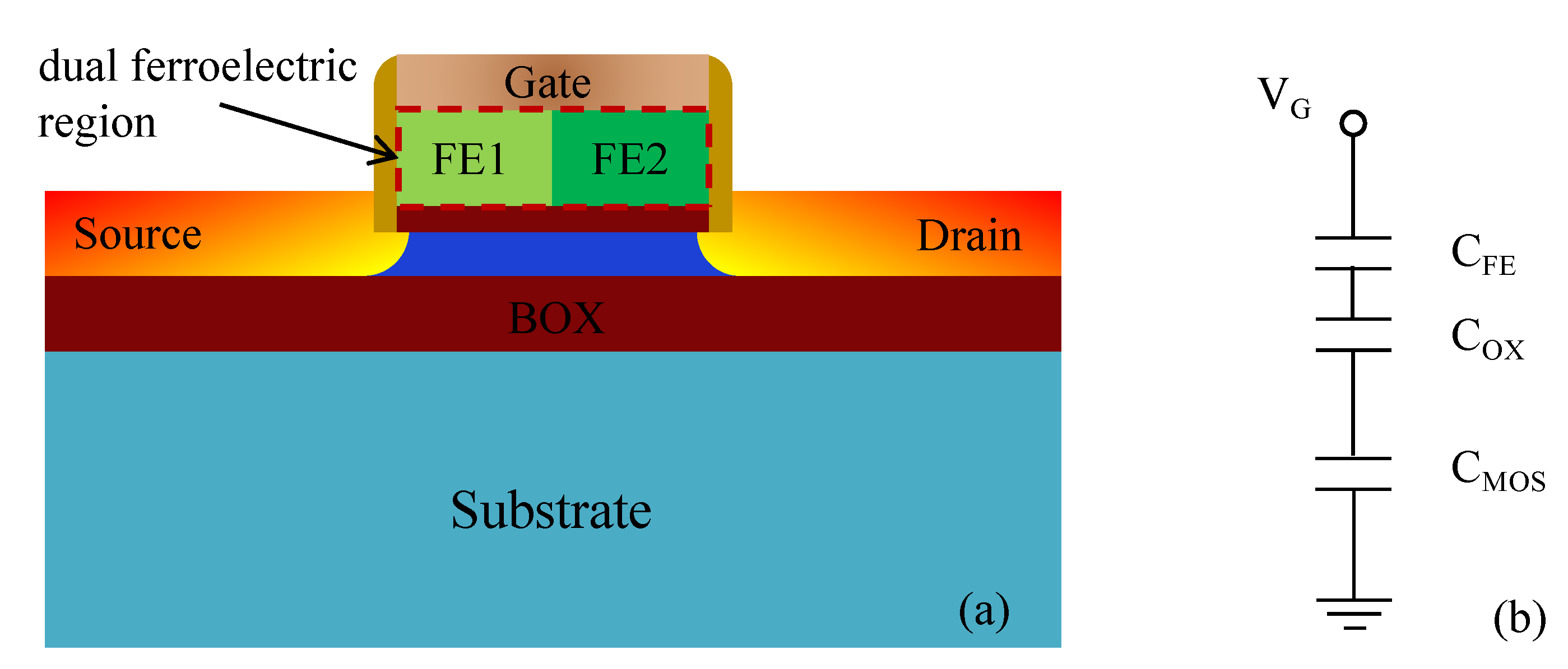
The schematic of the new DFR-NCFET based on the FDSOI structure is shown in
Figure 1a. Compared with the traditional FDSOI NCFET, the ferroelectric layer is composed of two ferroelectric materials (FE1 and FE2) in the proposed DFR-NCFET. By changing the ferroelectric parameters in different regions of the ferroelectric layer, the DFR-NCFET obtains a non-uniform voltage amplification effect by the dual ferroelectric layer, which significantly improves the control ability of the gate to the channel and optimizes the subthreshold swing of negative capacitance transistors.
The equivalent capacitance model of the NCFET is given in
Figure 1b, where the C
FE, C
OX and C
MOS are the capacitance of the ferroelectric layer, gate oxide layer, and MOS structure, respectively. Equation (1) is the formula for calculating the ferroelectric layer capacitance [
3].
where the T
FE is the thickness, Q is the surface net charge, α, β, and γ are the intrinsic parameters of ferroelectric layer, which are typically extracted from measurements. α, β, and γ are determined by the orientation of the ferroelectric material along the lattice, the periodicity and sparsity of the atomic arrangement. According to Equation (1), the increasing absolute value of negative ferroelectric parameter |α| makes the absolute value of negative capacitance of ferroelectric layer (|C
FE|) decreasing, and since C
FE is negative, C
FE increases with the increasing|α|. As the positive ferroelectric parameter β increases, the absolute value of negative capacitance of ferroelectric layer (|C
FE|) increases continuously, so that the C
FE decreases. Combined with the NCFET equivalent capacitance model in
Figure 1b, the total negative capacitance transistor gate capacitance is
CFE+
COX, so the gate capacitance of the DFR-NCFET exhibits an increase with the absolute value of the ferroelectric parameter α and a decrease with the ferroelectric parameter β.
The T2 type material is the secondary phase transition ferroelectric material with the negative ferroelectric parameter α and positive ferroelectric parameters β and γ, where γ is much larger than|α|. When the ferroelectric material is T2 type material, the polynomial with γ can be ignored according to the Landua–Ginzburg–Devonshire (LGD) phenomenological theory. Then, the remanent polarization intensity P
r of the ferroelectric material at this time can be represented by the ferroelectric material parameters α and β, as shown in Equation (2).
Equation (2) shows that the remanent polarization intensity Pr increases as the ferroelectric parameter |α| increases, and the remanent polarization intensity Pr of ferroelectric materials decreases as the ferroelectric parameter β increases.
In this paper, the ferroelectric parameters of the conventional ferroelectric region are defined as α = −5.81 ×
cm/F, β = 3.29 ×
cm
5/(
), and γ = 2.17 ×
cm
9/(
) [
7]. The ferroelectric parameters of the FE1 region follows these parameters. In addition, the ferroelectric parameters of FE2 region are variable. Firstly, the α of FE2 is changed to
= −7 ×
cm/F,
= −8 ×
cm/F,
= −9 ×
cm/F, and
= −10 ×
cm/F, while keeping the remaining parameters such as ferroelectric parameters β and γ the same as the FE1 region. Then, the β of FE2 is changed to
= 1.645 ×
cm
5/(FC
2),
= 3.29 ×
cm
5/(FC
2),
= 1.645 ×
cm
5/(FC
2), and
= 3.29 × 10
21 cm
5/(FC
2) while keeping the remaining parameters such as ferroelectric parameters α and γ the same as the FE1 region. The thickness of the ferroelectric region (T
FE) of the dual ferroelectric region is fixed at 10 nm, and the other structural parameters of the negative capacitance transistor are given in
Table 1.
3. Voltage Amplification Effect
To investigate the voltage amplification effect of the dual ferroelectric region in DFR-NCFET, conventional ferroelectric region NCFET (CFR-NCFET) and DFR-NCFET are performed in this section using the Sentaurus TCAD. The ferroelectric models are used in the simulation, so that the dual ferroelectric region exhibits the ferroelectric hysteresis effect and negative capacitance effect accordingly.
Figure 2 shows the potential distributions of the ferroelectric region of the CFR-NCFET and the DFR-NCFET device at V
GS = 1 V and V
DS = 0.4 V. The ferroelectric parameter α is −5.81×
cm/F for the conventional ferroelectric layer, while α is −5.81×
cm/F and −8×
cm/F of the FE1 region and FE2 region for the dual ferroelectric region. It can be seen that the potential distribution of the conventional ferroelectric layer is basically symmetrical. For the dual ferroelectric region, the potential at the bottom of the ferroelectric region is higher and the potential lines are more densely distributed in the FE2 region. The reason is the different region with different ferroelectric parameters causes different ferroelectric capacitances, which results in a different body factor and increased potential distribution from FE1 region to FE2 region. Therefore, the negative capacitance dual ferroelectric region exhibits non-uniform voltage amplification, which greatly enhances the gate voltage control compared to the CFR-NCFET.
Figure 3 shows the potential distributions of the ferroelectric region for the CFR-NCFET and the DFR-NCFET with variable β. The ferroelectric parameter β of the ferroelectric region in the CFR-NCFET and the FE1 region in the DFR-NCFET is 3.29 ×
cm
5/(
), and it is 3.29 ×
cm
5/(
) in the FE2 region of the DFR-NCFET. The figure shows that for the dual ferroelectric region, the potential value at the bottom of the ferroelectric layer decreases with the increase in β in FE2, and the distribution of potential lines within the ferroelectric region is sparser. Therefore, the voltage amplification effect of the dual ferroelectric region with an increased β in FE2 is weakened compared to the conventional ferroelectric region.
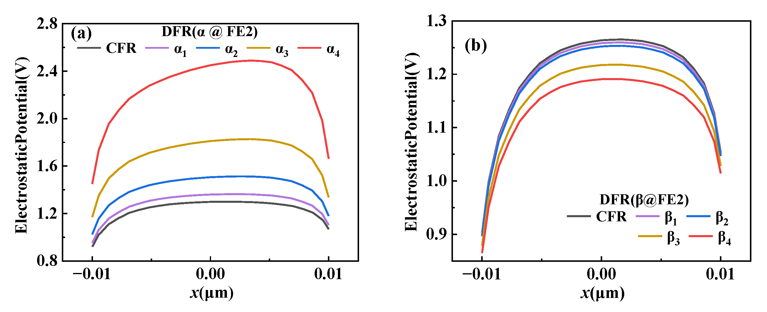
To explicitly show the voltage amplification effect,
Figure 4 shows the voltage profile along the bottom of the ferroelectric region when the voltage of 1 V applied on the gate. As shown in
Figure 4a, the non-uniform voltage amplification effect was observed for the DFR-NCFET, and the voltage near the drain is higher than the voltage near the source. This is because the voltages in the FE1 and FE2 regions are amplified simultaneously, but not at the same amplification value. When the α of FE2 is increased, the non-uniform voltage amplification effect is more obvious. The voltage can be amplified by up to 2.5 times for the dual ferroelectric region. While the voltage is amplified by a factor of 1.2 for the conventional ferroelectric region. As can be seen in
Figure 4b, the increase in β in FE2 leads to the decrease in the voltage amplification, but the influence is very small.
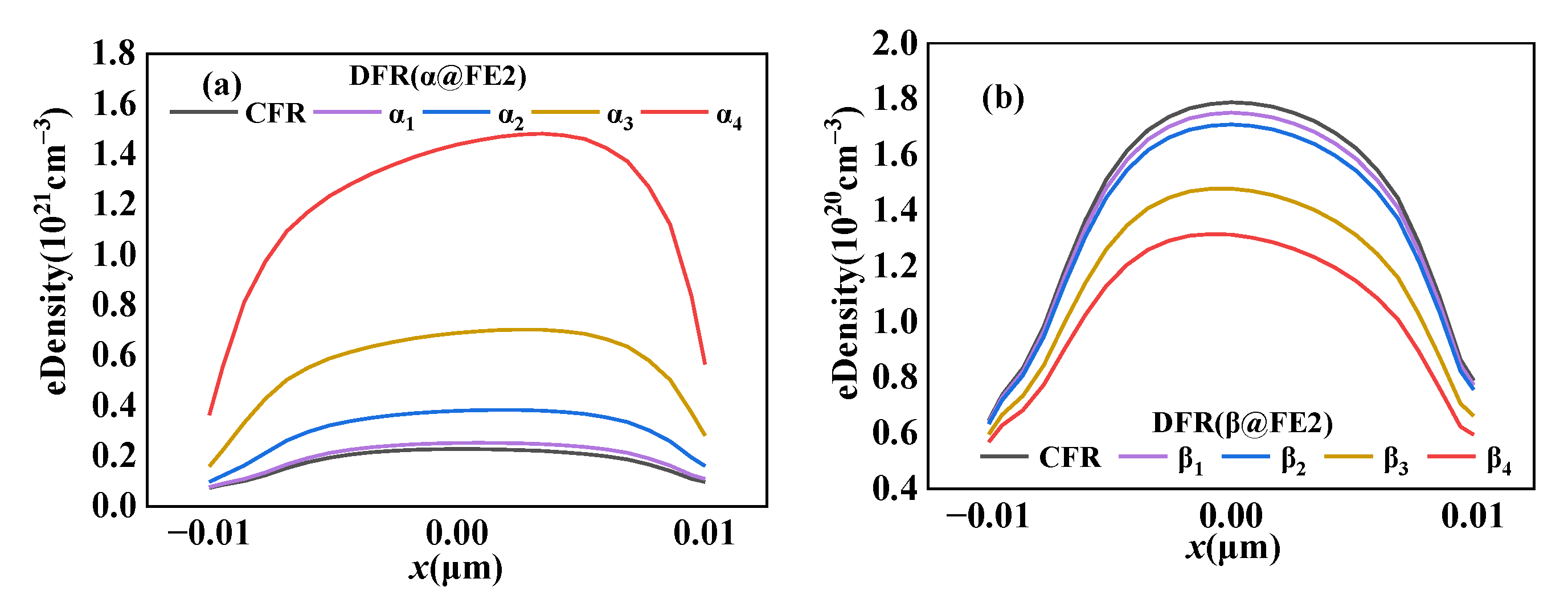
The channel surface electron concentration distribution of the CFR-NCFET and the DFR-NCFET in the on state is given in
Figure 5. The channel doping concentration is 1×10
17 cm
−3 when the transistor is in the off state.
Figure 5a shows the electron density depends on the α of FE2 and
Figure 5b shows the electron density depends on the β of FE2. Because of the non-uniform voltage amplification effect caused by the dual ferroelectric region, the electron concentration on the channel surface has distributions similar to the voltage distributions shown in
Figure 4. The figures also show that the conductive carrier concentration of the channel increases significantly with the increase in the absolute value of α, while it decreases with the increase in the ferroelectric parameter β of FE2.
The polarization intensity along the bottom of the ferroelectric region for the DFR-NCFET in the on/off state is given in
Figure 6. From
Figure 6, it can be seen that the polarization intensity in each transistor is almost the same when the transistor is under the off state, while the polarization intensity flips from negative to positive during the transistor operating from the off state to the on state. In
Figure 6a, a significant increase in the on-state polarization intensity with the increase in α, and the non-uniformity of the polarization intensity also increased, the polarization intensity reaches a value of 7.4 × 10
−6 C/cm
2 in FE1 and 8.4 × 10
−6 C/cm
2 in FE2, which is much higher than the 2.1 × 10
−6 C/cm
2 of the CDR-NCFET. In
Figure 6b, the on-state polarization intensity decreases with the increase in the ferroelectric parameter β in FE2, the on-state polarization intensity is 1.8 × 10
−6 C/cm
2 in FE1 and 1.6 × 10
−6 C/cm
2 in FE2 for the DFR-NCFET with β
4. The polarization flip in
Figure 6 is consistent with the voltage amplification in
Figure 4, reflecting that the polarization flip of the ferroelectric region is the fundamental reason for determining the voltage amplification.
4. Results and Discussions
Based on the non-uniform voltage amplification effect of the dual ferroelectric region, the influences of this effect on the NCFET characteristics are investigated and discussed in this section.
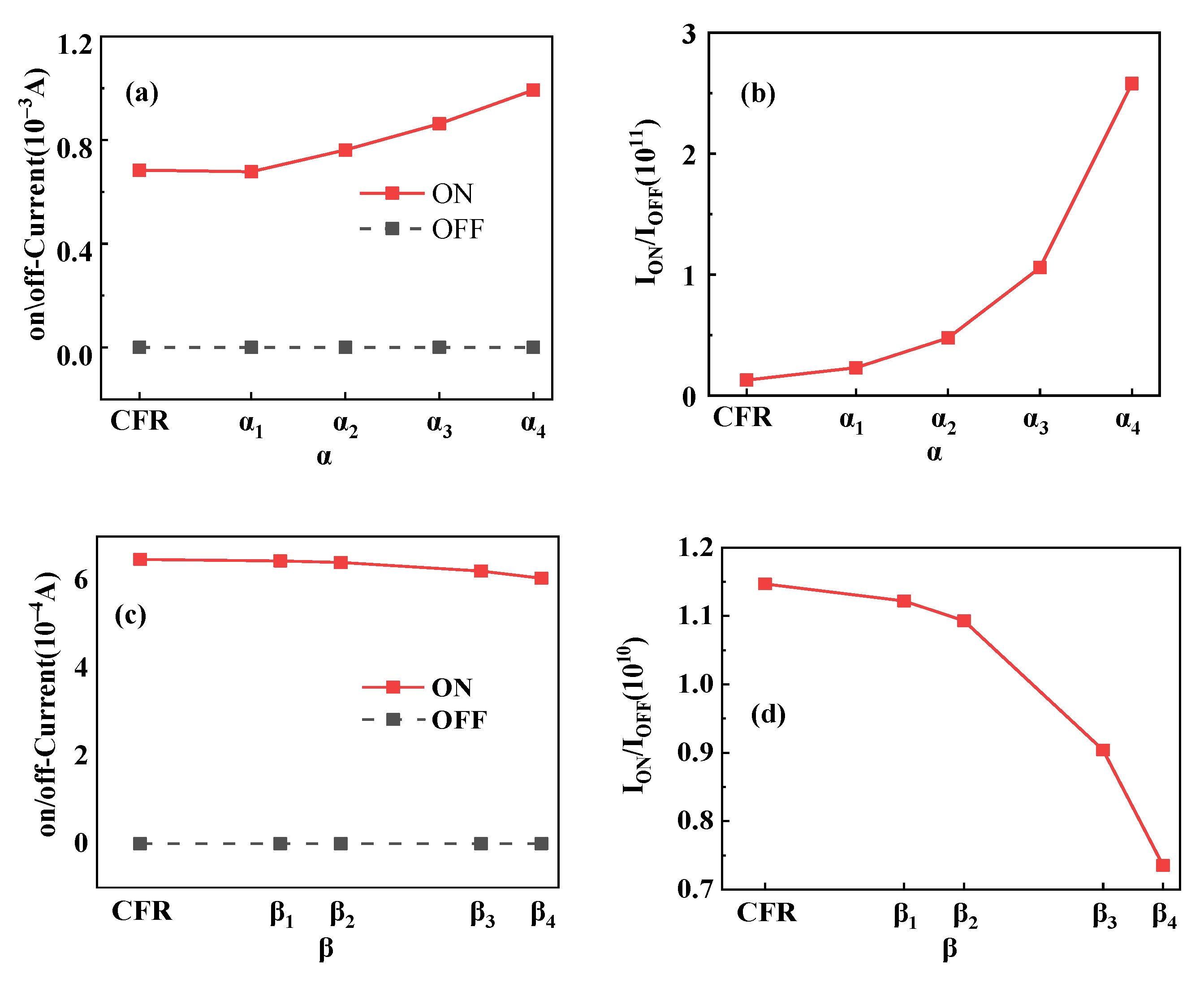
Figure 7 shows the on/off state current and on/off current ratio of the DFR-NCFET with different ferroelectric parameters. The on-state current increases with the increase in the absolute value of the ferroelectric parameter α in
Figure 7a, and the on-state current decreases with the increase in the ferroelectric parameter β in
Figure 7c, which is consistent with the trend of the change in the channel surface electron concentration with the change in the ferroelectric parameters α and β during the transistor’s on state in
Figure 5. The on/off current ratio of DFR-NCFET with different ferroelectric parameters α in
Figure 7b also shows a trend of increasing with the absolute value of ferroelectric parameter α. The on/off current ratio reflects the control capability of a transistor gate voltage for the channel, and it is obvious that the gate voltage control capability of DFR-NCFET with variable α ferroelectric layer becomes stronger and stronger as the absolute value of ferroelectric parameter α increases. The on/off current ratio of DFR-NCFET with different ferroelectric parameters β in
Figure 7d shows a trend of decreasing with increasing ferroelectric parameters β. The on/off current ratio shows that the channel control ability of variable β ferroelectric layer DFR-NCFET is weaker than that of conventional negative capacitance transistors.
Figure 8 shows the output characteristics curves of the DFR-NCFET compared to the CFR-NCFET with the gate-source voltages (
VGS) of 0.3 V, 0.6 V, 0.9 V, 1.2 V, and 1.5 V. From
Figure 8a, it can be seen that the DFR-NCFET has higher current in the saturation region when compared to the CFR-NCFET. Which is because of the stronger voltage amplification effect of the dual ferroelectric region. It also can be seen that the saturation current becomes higher as the absolute value of the ferroelectric parameter α is increased. The maximum amplification of the saturation current of the DFR-NCFET reaches 1.53 times of the CFR-NCFET. However,
ID trends to be the same when the drain voltage is large enough. The reason is the polarization of ferroelectric layer will be affected by drain voltage under the constant gate voltage, thus inhibiting the effect of NC voltage amplification. Moreover, the potential on the channel surface is decreased with the increase in drain voltage, which leading to the decrease in
ID in the output characteristic curve. In
Figure 8b, the saturation current of the DFR-NCFET with large β is smaller than the CFR-NCFET, but almost the same at smaller gate-source voltage of larger drain voltage.
Figure 9 shows the drain induced barrier lower (DIBL) extraction results of the CFR-NCFET and DFR-NCFET with different α and β of FE2. It is obvious from
Figure 9a that the negative DIBL of the DFR-NCFET becomes more and more obvious as the absolute value of the ferroelectric parameter α increases. This implies that the DFR-NCFET is increasingly capable of combating short-channel effects as the absolute value of the ferroelectric parameter α increases, thus have great application prospects for short-channel devices. However, it is obvious from
Figure 9b that the negative DIBL phenomenon of the DFR-NCFET becomes weaker as the ferroelectric parameter β increases, which means that the DFR-NCFET becomes less capable of combating short-channel effects as the ferroelectric parameter β increases.
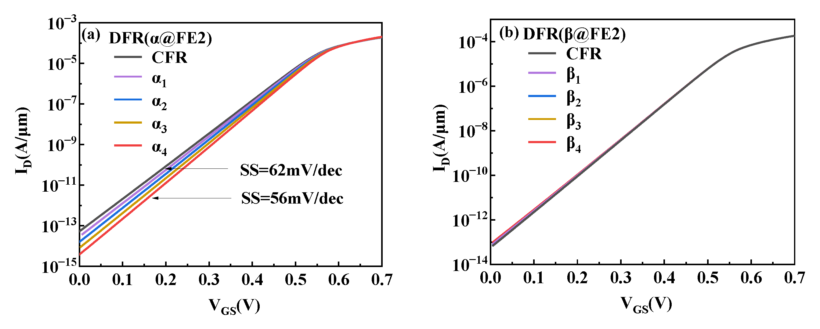
Figure 10 shows the transfer characteristic curves of the DFR-NCFET compared with the CFR-NCFET with a drain voltage of 0.4 V for each transistor. As can be seen in
Figure 10a, with the increasing absolute value of the ferroelectric parameter α, the drain current decreases, and the subthreshold swing (SS) of the DFR-NCFET decreases, and as the ferroelectric parameter α increases from α = −5.81 × 10
10 cm/F to α
4 = −1×10
11 cm/F, the subthreshold swing of the negative capacitor transistor decreases from 62 mV/dec to 56 mV/ dec, breaking the subthreshold swing limit of 60 mV/dec. It can be seen in
Figure 10b that the subthreshold swing of the DFR-NCFET increases slightly with the increase in the absolute value of the ferroelectric parameter β. With the increase in the ferroelectric parameter β, the subthreshold swing of the transistor increases from 61.7 mV/dec to 62.4 mV/dec, so the ferroelectric parameter β has little effect on the transistor performance.
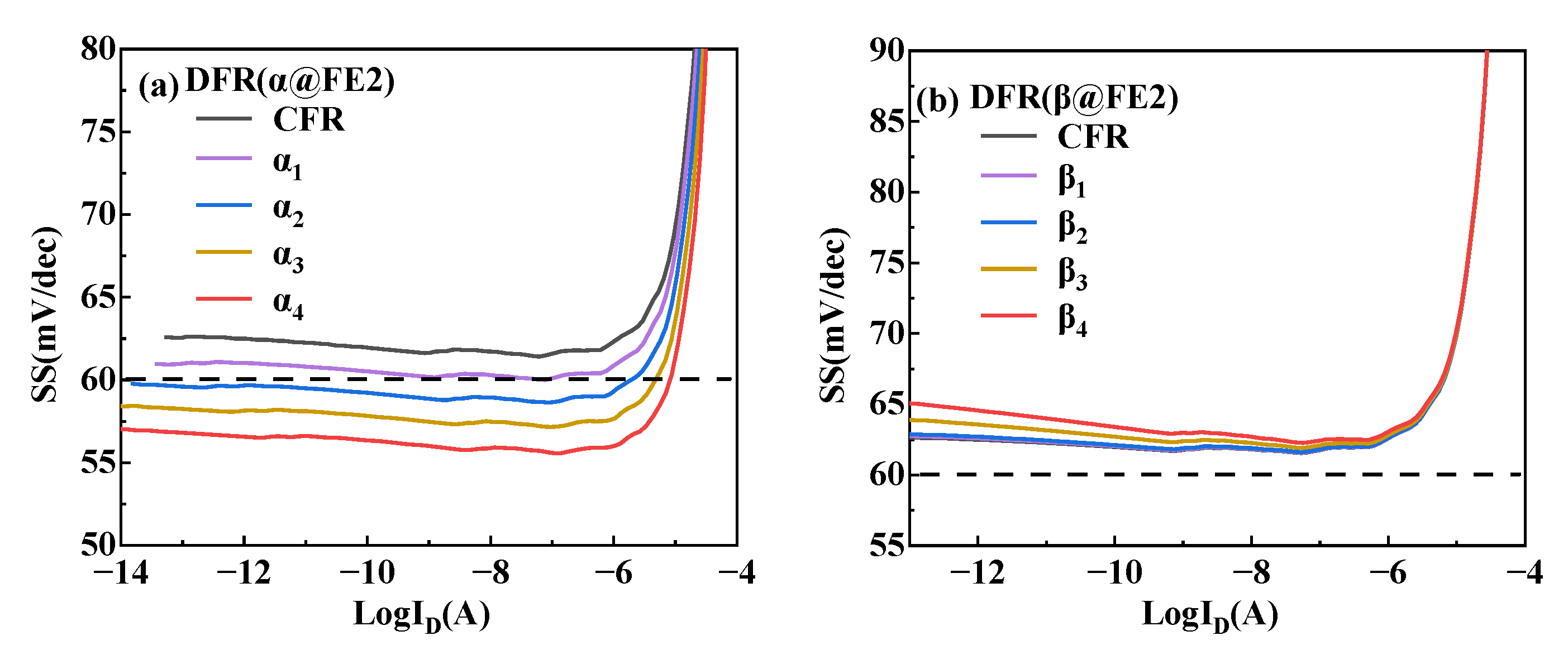
The subthreshold swing versus current for the DFR-NCFET is given in
Figure 11. As seen in
Figure 11a, after the ferroelectric parameter α reaches α
2 = −8 × 10
10 cm/F, the subthreshold swing of the DFR-NCFET is below 60 mV/dec throughout the subthreshold region, and it can be seen that the subthreshold swing increases rapidly as the current increases beyond the subthreshold region. Thus DFR-NCFET is able to obtain a subthreshold swing below the Boltzmann limit (60 mV/dec) by increasing the ferroelectric parameter α of FE2. From
Figure 11b, it can be seen that the variable β ferroelectric layer DFR-NCFET has a subthreshold swing above the Boltzmann limit (60 mV/dec) throughout the subthreshold region, and it is more obvious that the subthreshold swing of the DFR-NCFET increases slightly with the increase in the ferroelectric parameter β.
5. Conclusions
In this paper, a novel DFR-NCFET is proposed and investigated with numerical results obtained from the Sentaurus TCAD tool. First, the device structure is described, and its mechanism is explained. The dual ferroelectric region FE1 and FE2 have different ferroelectric parameters α and β, resulting in a non-uniform voltage amplification effect. Then, the effect of non-uniform voltage amplification phenomenon on the performances of the negative capacitance transistors is investigated, such as the potential distribution of the ferroelectric region, the voltage distribution, the electron concentration distribution, and the on/off state ferroelectric polarization intensity distribution along the bottom of the ferroelectric region with variable α and β in FE2 region. Thirdly, the influences of the non-uniform voltage amplification effect on the NCFET’s characteristics are investigated and discussed. The simulation results indicate that with an increasing absolute value of the ferroelectric parameter α, the saturation current becomes higher and reaches 1.53 times at the maximum saturation current compared to the CFR-NCFET. Meanwhile, the negative DIBL of the DFR-NCFET becomes more and more obvious. Furthermore, the SS of the DFR-NCFET decreases, and breaks the subthreshold swing limit of 60 mV/dec. For the ferroelectric parameter β, it will reduce the non-uniform voltage amplification effect and negative capacitance transistor performance with increasing ferroelectric parameter β. These results provide the guidance for the selection of ferroelectric materials for the design of the DFR-NCFET.
