
Variation of Surface Nanostructures on (100) PbS Single Crystals during Argon Plasma Treatment

 , and
, and 
Abstract
1. Introduction
2. Materials and Methods
3. Results and Discussion
3.1. Sputtering Rates of PbS Single Crystals in Argon Plasma with Varying Ar+ Ion Energy
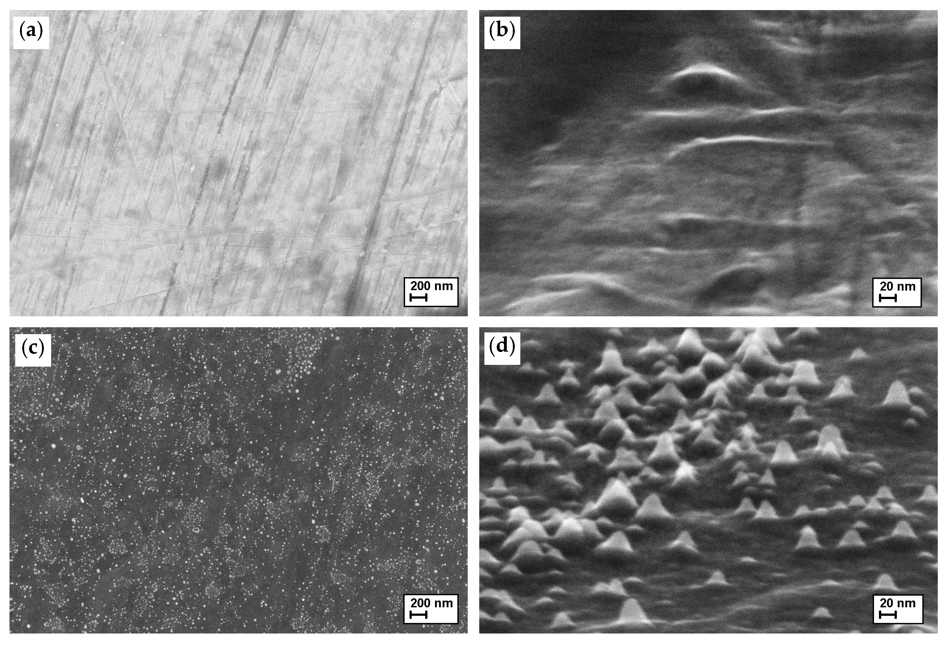
3.2. Formation of Nanotips via the Micromasking Mechanism
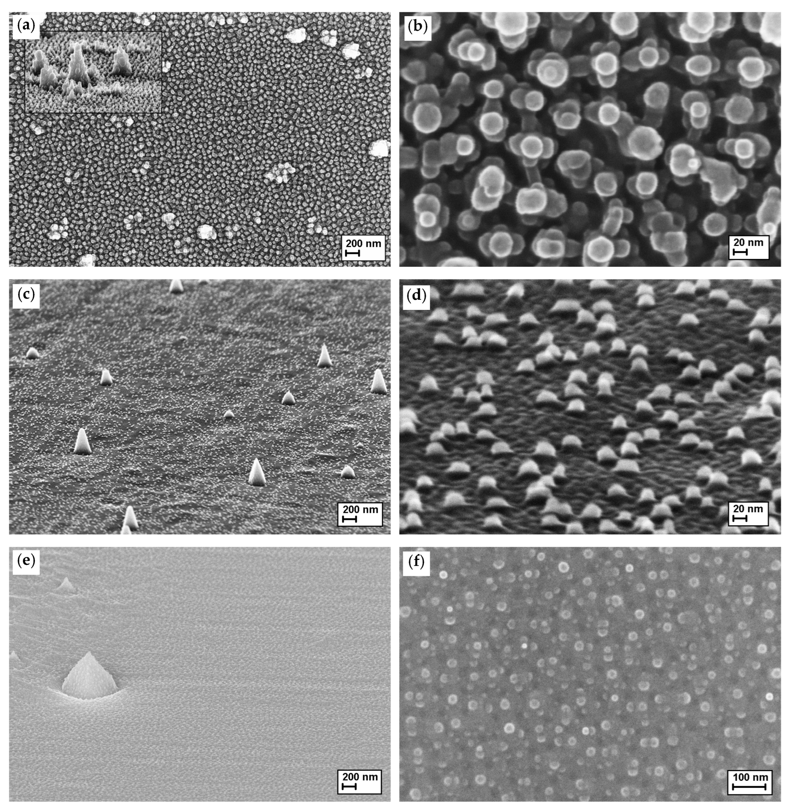
3.3. Submicron Cones and Arrays of Nanostructures
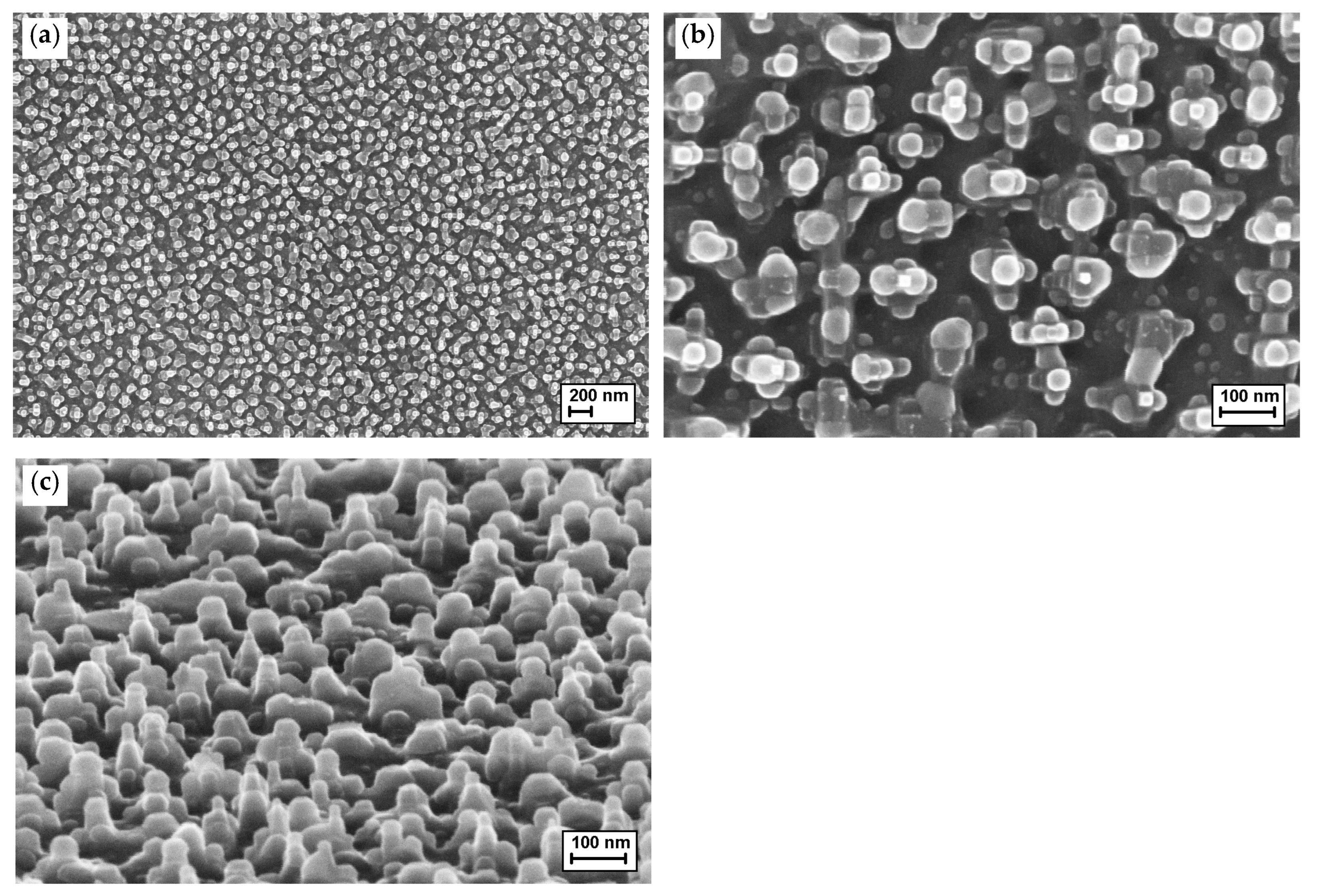
3.4. Formation of Nanostructure Arrays without Submicron Cones
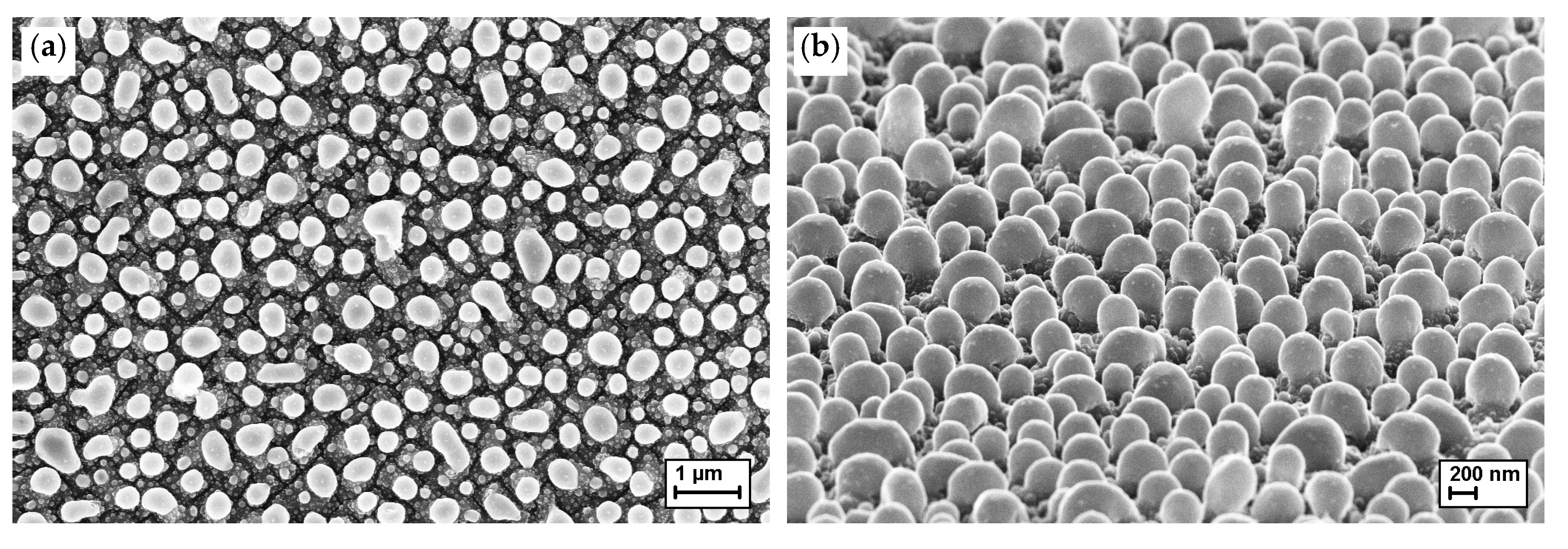
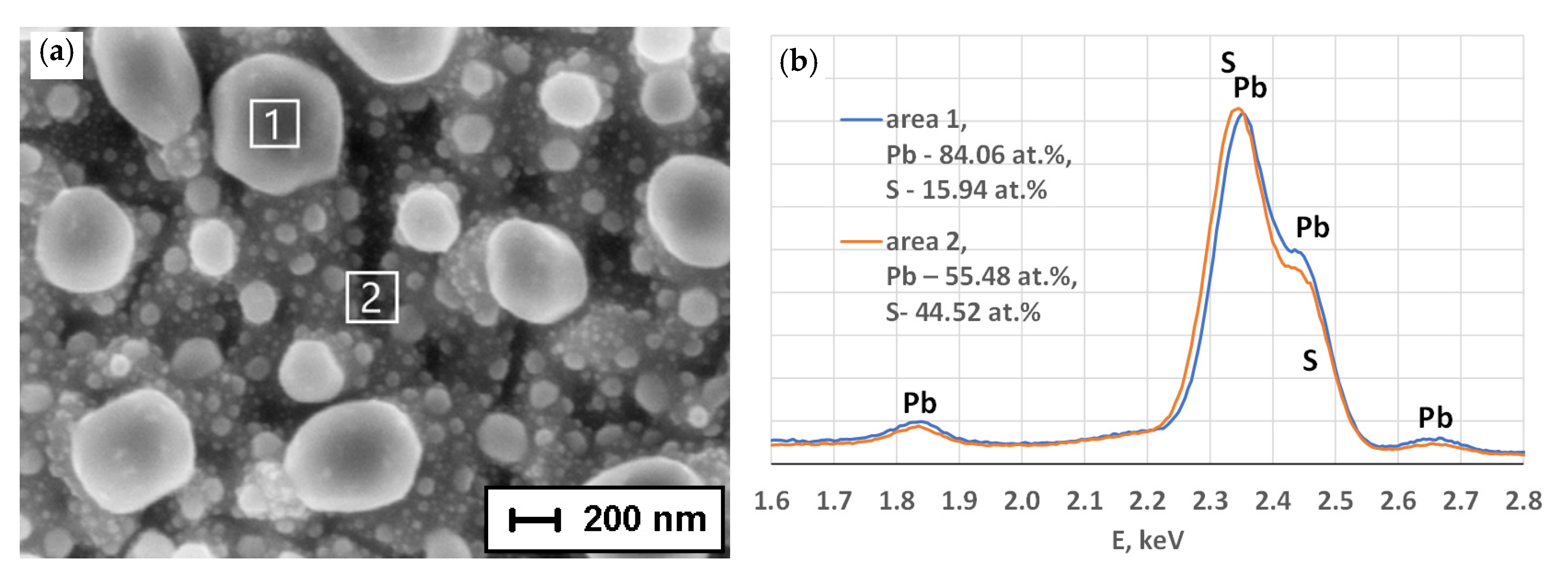
3.5. Formation of Quasi-Spherical Lead Submicron Structures
4. Conclusions
Author Contributions
Funding
Data Availability Statement
Acknowledgments
Conflicts of Interest
References
- Xiao, G.; Wang, Y.; Ning, J.; Wei, Y.; Liu, B.; William, W.Y.; Zou, G.; Zou, B. Recent advances in IV–VI semiconductor nanocrystals: Synthesis, mechanism, and applications. RSC Adv. 2013, 3, 8104–8130. [Google Scholar] [CrossRef]
- Litvin, A.P.; Martynenko, I.V.; Purcell-Milton, F.; Baranov, A.V.; Fedorov, A.V.; Gun’Ko, Y.K. Colloidal quantum dots for optoelectronics. J. Mater. Chem. A 2017, 5, 13252–13275. [Google Scholar] [CrossRef]
- Wang, L.; Wang, Y.; Jia, Y.; Liu, X.; Liu, T.; Fu, T.; Li, J.; Weng, B.; Zhang, X.; Liu, Y. Manipulation of Phase-Transfer Ligand-Exchange Dynamics of PbS Quantum Dots for Efficient Infrared Photovoltaics. J. Phys. Chem. C 2019, 123, 30137–30144. [Google Scholar] [CrossRef]
- Zhang, X.; Zhang, J.; Phuyal, D.; Du, J.; Tian, L.; Öberg, V.A.; Johansson, M.B.; Cappel, U.B.; Karis, O.; Liu, J.; et al. Inorganic CsPbI3 perovskite coating on PbS quantum dot for highly efficient and stable infrared light converting solar cells. Adv. Energy Mater. 2018, 8, 1702049. [Google Scholar] [CrossRef]
- Sukharevska, N.; Bederak, D.; Goossens, V.M.; Momand, J.; Duim, H.; Dirin, D.N.; Kovalenko, M.V.; Kooi, B.J.; Loi, M.A. Scalable PbS Quantum Dot Solar Cell Production by Blade Coating from Stable Inks. ACS Appl. Mater. Interfaces 2021, 13, 5195–5207. [Google Scholar] [CrossRef]
- Jana, S.; Goswami, S.; Nandy, S.; Chattopadhyay, K.K. Synthesis of tetrapod like PbS microcrystals by hydrothermal route and its optical characterization. J. Alloy. Compd. 2009, 481, 806–810. [Google Scholar] [CrossRef]
- Murray, C.B.; Sun, S.; Gaschler, W.; Doyle, H.; Betley, T.A.; Kagan, C.R. Colloidal synthesis of nanocrystals and nanocrystal superlattices. IBM J. Res. Dev. 2001, 45, 47–56. [Google Scholar] [CrossRef]
- Bakueva, L.; Gorelikov, I.; Musikhin, S.; Zhao, X.S.; Sargent, E.H.; Kumacheva, E. PbS quantum dots with stable efficient luminescence in the near-IR spectral range. Adv. Mater. 2004, 16, 926–929. [Google Scholar] [CrossRef]
- Alchalabi, K.; Zimin, D.; Kostorz, G.; Zogg, H. Self-assembled semiconductor quantum dots with nearly uniform sizes. Phys. Rev. Lett. 2003, 90, 026104. [Google Scholar] [CrossRef]
- Anthony, S.P.; Cho, W.J.; Lee, J.I.; Kim, J.K. Synthesis of lead chalcogenide nanoparticles in block copolymer micelles: Investigation of optical properties and fabrication of 2-D arrays of nanoparticles. J. Mater. Chem. 2009, 19, 280–285. [Google Scholar] [CrossRef]
- Dong, G.; Wu, B.; Zhang, F.; Zhang, L.; Peng, M.; Chen, D.; Wu, E.; Qiu, J. Broadband near-infrared luminescence and tunable optical amplification around 1.55 μm and 1.33 μm of PbS quantum dots in glasses. J. Alloy. Compd. 2011, 509, 9335–9339. [Google Scholar] [CrossRef]
- Zimin, S.; Gorlachev, E.; Amirov, I. Inductively Coupled Plasma Sputtering: Structure of IV-VI Semiconductors. In Encyclopedia of Plasma Technology, 1st ed.; Shohet, J.L., Ed.; CRC Press: New York, NY, USA, 2017; pp. 679–691. Available online: https://www.routledgehandbooks.com/doi/10.1081/E-EPLT-120053966 (accessed on 1 November 2020).
- Gago, R.; Vázquez, L.; Cuerno, R.; Varela, M.; Ballesteros, C.; Albella, J.M. Production of ordered silicon nanocrystals by low-energy ion sputtering. Appl. Phys. Lett. 2001, 78, 3316–3318. [Google Scholar] [CrossRef]
- Levchenko, I.; Ostrikov, K. Nanostructures of various dimensionalities from plasma and neutral fluxes. J. Phys. D: Appl. Phys. 2007, 40, 2308–2319. [Google Scholar] [CrossRef]
- Bradley, R.M.; Shipman, P.D. Spontaneous pattern formation induced by ion bombardment of binary compounds. Phys. Rev. Lett. 2010, 105, 145501. [Google Scholar] [CrossRef] [PubMed]
- Singh, U.B.; Agarwal, D.C.; Khan, S.A.; Kumar, M.; Tripathi, A.; Singhal, R.; Panigrahi, B.K.; Avasthi, D.K. Engineering of hydrophilic and plasmonic properties of Ag thin film by atom beam irradiation. Appl. Surf. Sci. 2011, 258, 1464–1469. [Google Scholar] [CrossRef]
- Tanyeli, I.; Marot, L.; Mathys, D.; van de Sanden, M.C.M.; De Temmerman, G. Surface modifications induced by high fluxes of low energy Helium ions. Sci. Rep. 2015, 5, 9779. [Google Scholar] [CrossRef] [PubMed]
- Sulania, I.; Agarwal, D.; Husain, M.; Avasthi, D.K. Investigations of ripple pattern formation on Germanium surfaces using 100-keV Ar+ ions. Nanoscale Res. Lett. 2015, 10, 88. [Google Scholar] [CrossRef]
- El-Said, A.S.; Wilhelm, R.A.; Heller, R.; Sorokin, M.; Facsko, S.; Aumayr, F. Tuning the fabrication of nanostructures by low-energy highly charged ions. Phys. Rev. Lett. 2016, 117, 126101. [Google Scholar] [CrossRef]
- Zimin, S.P.; Amirov, I.I.; Naumov, V.V.; Guseva, K.E. The Formation of Hollow Lead Structures on the Surface of PbSe Films Treated in Argon Plasma. Tech. Phys. Lett. 2018, 44, 518–521. [Google Scholar] [CrossRef]
- Zimin, S.P.; Amirov, I.I.; Naumov, V.V. Changes in the conductivity of lead-selenide thin films after plasma etching. Semiconductors 2016, 50, 1125–1129. [Google Scholar] [CrossRef]
- Zimin, S.P.; Gorlachev, E.S.; Amirov, I.I.; Zogg, H. Micromasking effect and nanostructure self-formation on the surface of lead chalcogenide epitaxial films on Si substrates during argon plasma treatment. J. Phys. D-Appl. Phys. 2009, 42, 165205. [Google Scholar] [CrossRef]
- Zimin, S.P.; Gorlachev, E.S.; Amirov, I.I.; Naumov, V.V.; Bagiyeva, G.Z. Application of abnormally high sputtering rate of PbTe (Te) single crystals during inductively coupled argon plasma treatment for fabrication of nanostructures. Semicond. Sci. Technol. 2015, 30, 035017. [Google Scholar] [CrossRef]
- Zimin, S.P.; Gorlachev, E.S.; Amirov, I.I.; Naumov, V.V.; Juskenas, R.; Skapas, M.; Abramof, E.; Rappl, P.H.O. Plasma-assisted surface nanostructuring of epitaxial Pb1−xSnxTe (0≤ x≤ 1) films. Semicond. Sci. Technol. 2019, 34, 095001. [Google Scholar] [CrossRef]
- Zimin, S.P.; Amirov, I.I.; Naumov, V.V.; Guseva, K.E. Surface Modification of Pb1–xSnxSe Films during Plasma Treatment Near the Sputtering Threshold. J. Surf. Ingestig.-X-Ray Synchro. 2020, 14, 1174–1178. [Google Scholar] [CrossRef]
- Zimin, S.P.; Gorlachev, E.S.; Gremenok, V.F.; Tsyrelchuk, I.N.; Naumov, V.V.; Amirov, I.I.; Dubov, G.A. Plasma sputtering of polycrystalline Pb1− xSnxTe thin films grown on glass substrates using hot wall deposition. Semicond. Sci. Technol. 2014, 29, 075020. [Google Scholar] [CrossRef]
- Zimin, S.P.; Gorlachev, E.S.; Amirov, I.I.; Naumov, V.V. Lead selenide nanowire growth by vapor-liquid-solid mechanism under mask during plasma processing. Tech. Phys. Lett. 2011, 37, 929–931. [Google Scholar] [CrossRef]
- Wang, Y.; Yang, X.; Xiao, G.; Zhou, B.; Liu, B.; Zou, G.; Zou, B. Shape-controlled synthesis of PbS nanostructures from− 20 to 240 °C: The competitive process between growth kinetics and thermodynamics. Crystengcomm 2013, 15, 5496–5505. [Google Scholar] [CrossRef]
- Lee, S.M.; Jun, Y.W.; Cho, S.N.; Cheon, J. Single-crystalline star-shaped nanocrystals and their evolution: Programming the geometry of nano-building blocks. J. Am. Chem. Soc. 2002, 124, 11244–11245. [Google Scholar] [CrossRef]
- Gerdes, F.; Volkmann, M.; Schliehe, C.; Bielewicz, T.; Klinke, C. Sculpting of lead sulfide nanoparticles by means of acetic acid and dichloroethane. Z. Phys. Chem. 2015, 229, 139–151. [Google Scholar] [CrossRef]
- Kolesnikov, N.N.; James, R.B.; Berzigiarova, N.S.; Kulakov, M.P. HPVB-and HPVZM-shaped growth of CdZnTe, CdSe, and ZnSe crystals. In X-Ray and Gamma-Ray Detectors and Applications IV, Proceedings of International Symposium on Optical Science and Technology, Seattle, WA, United States, 7–11 July 2002; James, R.B., Franks, L.A., Burger, A., Westbrook, E.M., Durst, R.D., Eds.; SPIE: Bellingham, WA, USA, 2003; Volume 4784, pp. 93–104. [Google Scholar] [CrossRef]
- Bohdansky, J.; Roth, J.; Bay, H.L. An analytical formula and important parameters for low-energy ion sputtering. J. Appl. Phys. 1980, 51, 2861–2865. [Google Scholar] [CrossRef]
- Zayachuk, D.M.; Slynko, V.E.; Csik, A. Peculiar properties of preferential sputtering of PbTe, SnTe, and GeTe by Ar+ ion plasma. Mater. Sci. Semicond. Process 2018, 88, 103–108. [Google Scholar] [CrossRef]
- Zimin, S.P.; Amirov, I.I.; Gorlachev, E.S. RF sputtering of epitaxial lead chalcogenide films in argon and krypton plasma. Semicond. Sci. Technol. 2011, 26, 055018. [Google Scholar] [CrossRef]
- Zimin, S.P.; Gorlachev, E.S.; Amirov, I.I.; Gerke, M.N.; Zogg, H.; Zimin, D. Role of threading dislocations during treatment of PbTe films in argon plasma. Semicond. Sci. Technol. 2007, 22, 929. [Google Scholar] [CrossRef]
- Cheng, C.; Fan, H.J. Branched nanowires: Synthesis and energy applications. Nano Today 2012, 7, 327–343. [Google Scholar] [CrossRef]
- Bierman, M.J.; Lau, Y.A.; Jin, S. Hyperbranched PbS and PbSe nanowires and the effect of hydrogen gas on their synthesis. Nano lett. 2007, 7, 2907–2912. [Google Scholar] [CrossRef] [PubMed]
- Bierman, M.J.; Jin, S. Potential applications of hierarchical branching nanowires in solar energy conversion. Energy Environ. Sci. 2009, 2, 1050–1059. [Google Scholar] [CrossRef]


| Ei (eV) | 25 | 75 | 100 | 200 |
| V (nm/s) | 0.1 | 3.3 | 5.8 | 10.8 |
| Ei (eV) | Plasma Treatment Duration (s) | Surface Micro- and Nanostructures | Formation Mechanism |
|---|---|---|---|
| 25 | 240–360 | Nanocones with 30–50 nm heights | Micromasking with Pb particles |
| 75 | 60 | 200 nm high submicron cones; nanodroplets with 50 nm diameters | Micromasking of dislocation exit sites; Pb droplet redeposition |
| 120 | 400 nm high submicron cones; orthogonal nanostructures with 50 nm nanodroplets | Micromasking of dislocation exit sites; VLS growth | |
| 180 | Arrays of larger quasi-spherical metallic structures; arrays of smaller quasi-spherical particles | Growth of hollow metallic Pb structures [20] | |
| 100, 200 | 60 | 350 nm high submicron cones; nanodroplets | Micromasking of dislocation exit sites; Pb droplet redeposition |
| 120 | 700 nm high submicron cones; cruciform nanostructures with 35 nm nanodroplets | Micromasking of dislocation exit sites; VLS growth | |
| 200 | 120 + 180 | Array of cruciform nanostructures with heights up to 140 nm with 25–70 nm nanodroplets | VLS growth |
Publisher’s Note: MDPI stays neutral with regard to jurisdictional claims in published maps and institutional affiliations. |
© 2022 by the authors. Licensee MDPI, Basel, Switzerland. This article is an open access article distributed under the terms and conditions of the Creative Commons Attribution (CC BY) license (https://creativecommons.org/licenses/by/4.0/).
Share and Cite
Zimin, S.P.; Kolesnikov, N.N.; Amirov, I.I.; Naumov, V.V.; Gorlachev, E.S.; Kim, S.; Kim, N.-H. Variation of Surface Nanostructures on (100) PbS Single Crystals during Argon Plasma Treatment. Crystals 2022, 12, 111. https://doi.org/10.3390/cryst12010111
Zimin SP, Kolesnikov NN, Amirov II, Naumov VV, Gorlachev ES, Kim S, Kim N-H. Variation of Surface Nanostructures on (100) PbS Single Crystals during Argon Plasma Treatment. Crystals. 2022; 12(1):111. https://doi.org/10.3390/cryst12010111
Chicago/Turabian StyleZimin, Sergey P., Nikolai N. Kolesnikov, Ildar I. Amirov, Viktor V. Naumov, Egor S. Gorlachev, Sara Kim, and Nam-Hoon Kim. 2022. "Variation of Surface Nanostructures on (100) PbS Single Crystals during Argon Plasma Treatment" Crystals 12, no. 1: 111. https://doi.org/10.3390/cryst12010111
APA StyleZimin, S. P., Kolesnikov, N. N., Amirov, I. I., Naumov, V. V., Gorlachev, E. S., Kim, S., & Kim, N.-H. (2022). Variation of Surface Nanostructures on (100) PbS Single Crystals during Argon Plasma Treatment. Crystals, 12(1), 111. https://doi.org/10.3390/cryst12010111