Article

Pressure-Induced Structural Phase Transition and Metallization in Ga2Se3 Up to 40.2 GPa under Non-Hydrostatic and Hydrostatic Environments

1
Key Laboratory of High-Temperature and High-Pressure Study of the Earth’s Interior, Institute of Geochemistry, Chinese Academy of Sciences, Guiyang 550081, China
2
University of Chinese Academy of Sciences, Beijing 100049, China
3
Shandong Provincial Key Laboratory of Water and Soil Conservation and Environmental Protection, College of Resources and Environment, Linyi University, Linyi 276000, China
*
Authors to whom correspondence should be addressed.
Crystals 2021, 11(7), 746; https://doi.org/10.3390/cryst11070746
Submission received: 8 June 2021 / Revised: 22 June 2021 / Accepted: 24 June 2021 / Published: 26 June 2021
(This article belongs to the Special Issue Superconductivity at High Pressure)

Abstract

:
A series of investigations on the structural, vibrational, and electrical transport characterizations for Ga2Se3 were conducted up to 40.2 GPa under different hydrostatic environments by virtue of Raman scattering, electrical conductivity, high-resolution transmission electron microscopy, and atomic force microscopy. Upon compression, Ga2Se3 underwent a phase transformation from the zinc-blende to NaCl-type structure at 10.6 GPa under non-hydrostatic conditions, which was manifested by the disappearance of an A mode and the noticeable discontinuities in the pressure-dependent Raman full width at half maximum (FWHMs) and electrical conductivity. Further increasing the pressure to 18.8 GPa, the semiconductor-to-metal phase transition occurred in Ga2Se3, which was evidenced by the high-pressure variable-temperature electrical conductivity measurements. However, the higher structural transition pressure point of 13.2 GPa was detected for Ga2Se3 under hydrostatic conditions, which was possibly related to the protective influence of the pressure medium. Upon decompression, the phase transformation and metallization were found to be reversible but existed in the large pressure hysteresis effect under different hydrostatic environments. Systematic research on the high-pressure structural and electrical transport properties for Ga2Se3 would be helpful to further explore the crystal structure evolution and electrical transport properties for other A2B3-type compounds.

1. Introduction

In recent decades, A2B3-type (A: Ga, In; B: S, Se, Te) metal chalcogenides have drawn considerable interest due to their extensive applications in the field of photovoltaic devices, IR detectors, and nuclear particle detection devices [1,2,3,4]. As an important member of the A2B3-type semiconductor, gallium sesquiselenide (Ga2Se3) crystallizes into a defective zinc-blende structure at ambient conditions, where one-third of the gallium sites in the crystal structure are vacant owing to the difference in the valence between gallium and selenium ions [5]. In light of its excellent performances of high energy conversion efficiency and large electrochemical capacity, Ga2Se3 has been widely applied to lithium-ion batteries, photocatalysts, and dilute magnetic semiconductors [6,7,8].
As usual, pressure is capable of modulating the atomic distances, positions, and interactions in most A2B3-type semiconducting compounds, and hence leads to some novel physical phenomena such as the pressure-induced structural transition, metallization, and amorphization [9,10,11,12,13]. As far as Ga2Se3 is concerned, its high-pressure phase stability and structural transition have been investigated by synchrotron X-ray diffraction, electrical resistance, and thermoelectric power [14,15]. Savchenko and Shchennikov (1994) performed the electrical resistance and thermoelectric power experiments for Ga2Se3 using a diamond anvil cell up to 35.0 GPa [14]. The authors found apparent discontinuities in the pressure-dependent electrical resistance and thermoelectric power at 14.2 GPa and attributed it to a semiconductor-to-semiconductor structural transition. Subsequently, Takumi et al. (2001) conducted the synchrotron X-ray diffraction on Ga2Se3 using the mixture of methanol, ethanol, and water (16:3:1 volume ratio) as the pressure medium and revealed that Ga2Se3 underwent a phase transition from the zinc-blende to NaCl-type structure at 14.0 GPa. Furthermore, the authors determined that the high-pressure phase is of NaCl-type structure by comparing the X-ray diffraction pattern from the high-pressure synchrotron experiment and theoretical calculation results [15]. More recently, the hydrostatic environment has been reported to play a vital role in the pressure point of structural transition for some A2B3-type metal dichalcogenides [9,13]. However, the influence of different hydrostatic environments on the structural and vibrational properties of Ga2Se3 remains rarely known till now. In addition, other A2B3-type metal chalcogenides belonging to the III–VI group (e.g., Ga2S3, Ga2Te3, In2S3, In2Se3, In2Te3, etc.) have been reported to undergo the semiconductor-to-metal phase transition under high pressure [12,13,16,17]. Therefore, it is worthwhile to explore whether Ga2Se3 exhibits metallic property under high pressure.
In this study, we report the structural transition and metallization for Ga2Se3 at pressures up to 40.2 GPa using a diamond anvil cell in conjunction with Raman scattering, AC complex impedance spectroscopy, high-resolution transmission electron microscopy, and atomic force microscopy. Furthermore, the influence of different hydrostatic environments on the phase transformation for Ga2Se3 is discussed in detail.

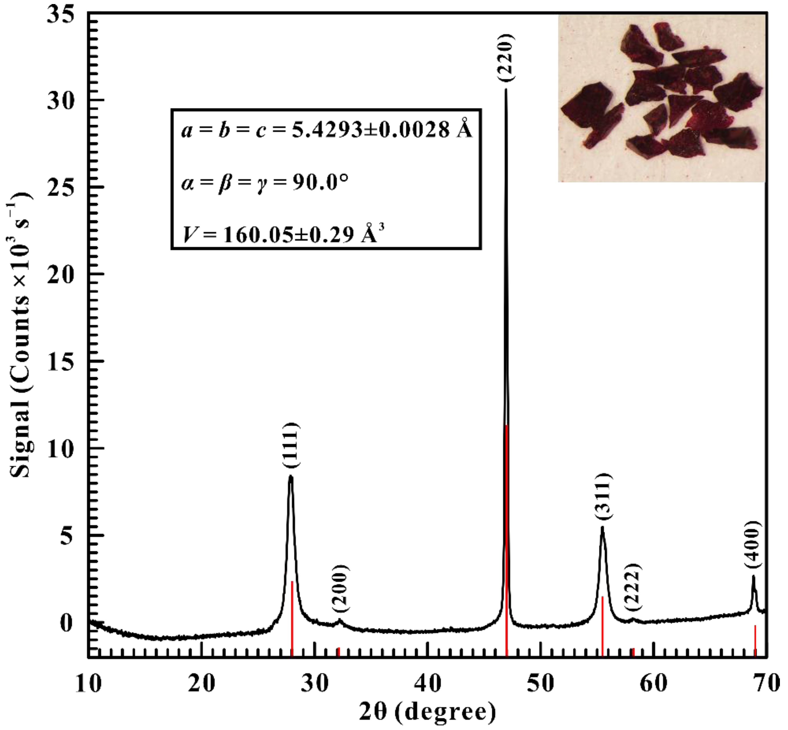
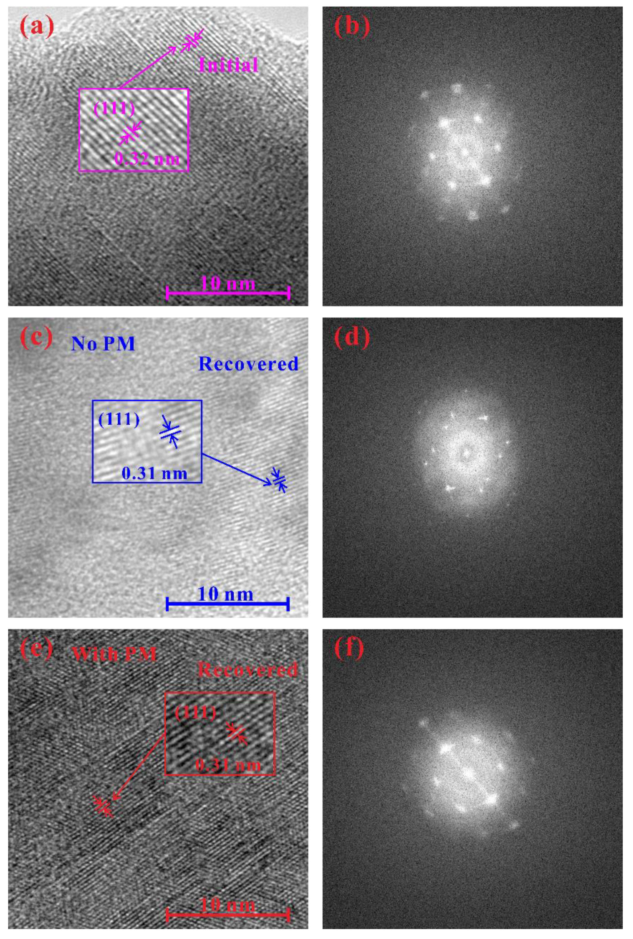
2. Materials and Methods

The commercially available Ga2Se3 sample (purity 99.999%), taking on dark red color (Figure 1), was bought from Hangzhou Kaiyada Semiconductor Material Co., Ltd., (Zhejiang, China). The phase identification of the initial sample was performed by X-ray diffraction (XRD) analysis using an Empyrean-type X-ray powder diffractometer with Cu Kα radiation under the operating conditions of 45 kV accelerating voltage and 40 mA beam current. The representative XRD pattern of the initial sample is displayed in Figure 1, and the result revealed that the initial sample belongs to a cubic structure of the F-43m space group (JCPDS no. 05-0724). We calculated the lattice parameters of the initial sample by using MDI Jade 6.5 software and obtained a = b = c = 5.4293 ± 0.0028 Å, α = β = γ = 90.0°, and V = 160.05 ± 0.29 Å3, which agrees well with the values taken from the standard JCPDS card.
High-pressure Raman scattering experiments were conducted using a diamond anvil cell (DAC) mounted with a culet diameter of 300 μm and bevel angle of 10°. A tiny ruby sphere with ~5 μm in size was employed as the pressure calibration based on the shift of the sharp R1 fluorescent peak, and the uncertainty of pressure calibration was less than 5%. In this study, Helium was adopted as the pressure medium to provide hydrostatic conditions, and no pressure medium was applied to attain non-hydrostatic conditions. In situ Raman scattering experiments were carried out by the Renishaw 2000 micro confocal Raman spectrometer equipped with a 785 nm diode laser. A suitable laser power of 5 mW was chosen to significantly improve the Raman signal of the sample and avoid destroying the sample through overheating. Raman spectra were collected within the wavenumber range of 100–400 cm−1 in backscattering configuration with the spectral resolution and integration time of 1.0 cm−1 and 120 s, respectively. The time interval of 15 min was controlled between each Raman scattering measurement to achieve pressure equilibrium. We obtained the Raman peak positions and full-width at half-maximums (FWHMs) by fitting the Raman spectra with a Lorenz-type function as implemented in PeakFit software.
High-pressure electrical conductivity measurements were performed with the same DAC that was utilized in our high-pressure Raman scattering experiments. A sheet of T-301 stainless steel gasket with the initial thickness of 250 μm was pre-indented into a thickness of ~40 μm, and then a hole of 180-μm diameter in the middle of the dent was drilled by the laser drilling machine. Successively, a mixture of boron nitride and epoxy serving as the insulating substance was fully covered and compacted into the hole, and another central hole with a diameter of ~100 μm was made as an insulating sample chamber. Two molybdenum electrodes were separately integrated into the upper and lower diamond anvils. No pressure medium was loaded into the sample chamber so as to ensure good electrical contact between sample and electrodes, as well as to avoid introducing additional errors during electrical conductivity measurements. AC complex impedance spectra were acquired using a Solartron-1260 impedance/gain phase analyzer with the predetermined frequency range of 10−1–107 Hz and signal voltage of 1.0 V. High-pressure temperature-variable electrical conductivity measurements were carried out by pressurizing the sample to the predesigned pressure points and then placing the DAC into the vessel filled with liquid Nitrogen refrigerant to obtain a low-temperature condition. Temperatures were monitored by using a k-type thermocouple with the ball head in direct contact with the diamond, and the precision of temperature measurement was ±5 K. More detailed descriptions of the high-pressure experimental technique and measurement procedures were reported elsewhere [9,10,13,18,19].
High-resolution transmission electron microscopy (HRTEM) observation for the initial sample and the recovered samples decompressed under non-hydrostatic and hydrostatic environments was conducted on a Tecnai G2 F20 S-TWIN TMP with an accelerating voltage of 200 kV. We uniformly dispersed the sample into ethanol by using an ultrasonic device and then transferred the formed solution onto a carbon-film-coated copper grid for HRTEM analysis. The interplanar spacings of the sample were accurately measured through Digital Micrograph software. In addition, the surface topography for the initial sample and the recovered samples were studied in detail by atomic force microscopy (AFM) observation using a Multimode 8 mass spectrometer in peak force tapping mode over the square-area scan size of 5.0 μm × 5.0 μm with the horizontal and vertical resolutions of 1.0 nm and 0.1 nm, respectively.

3. Results and Discussion

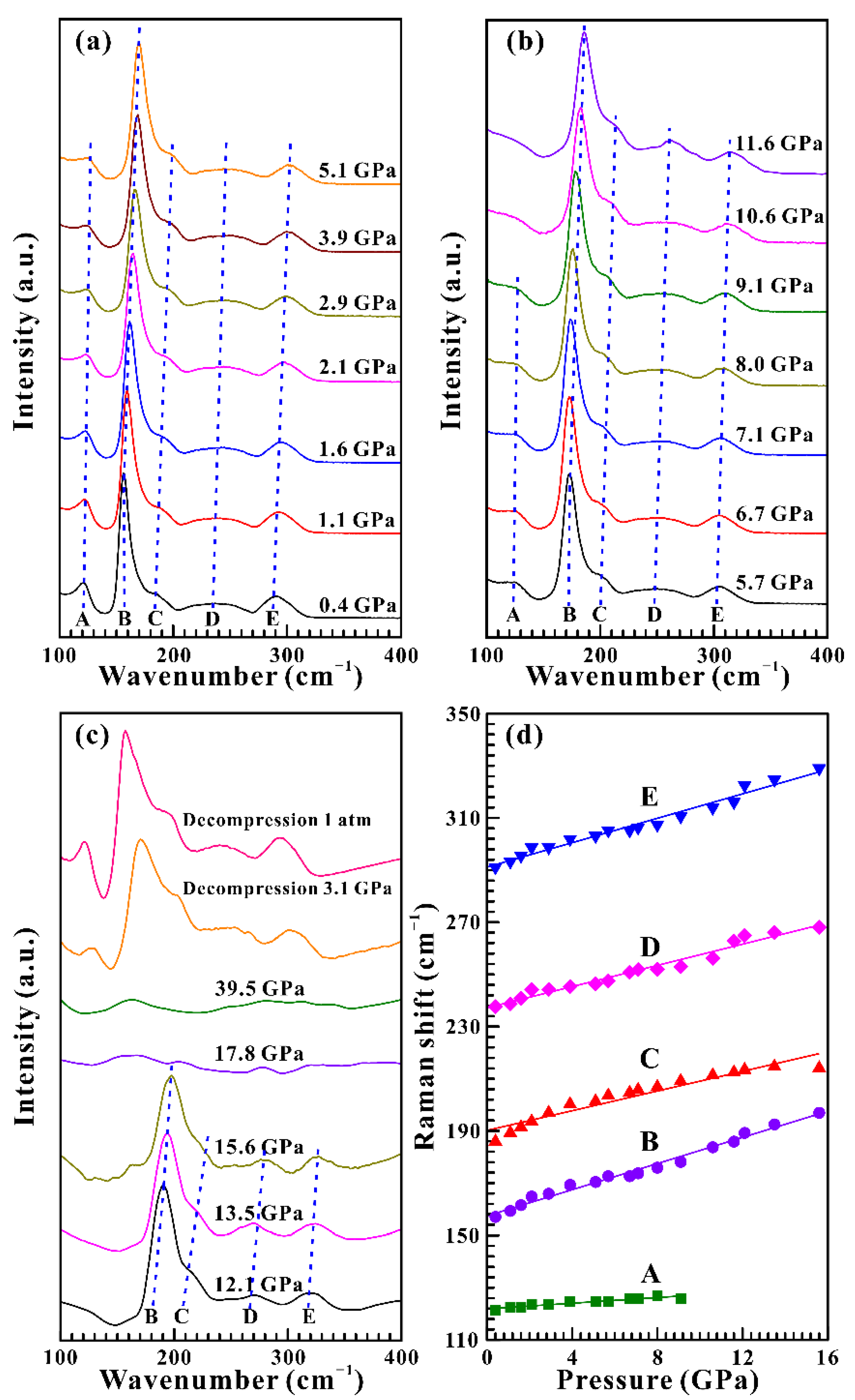
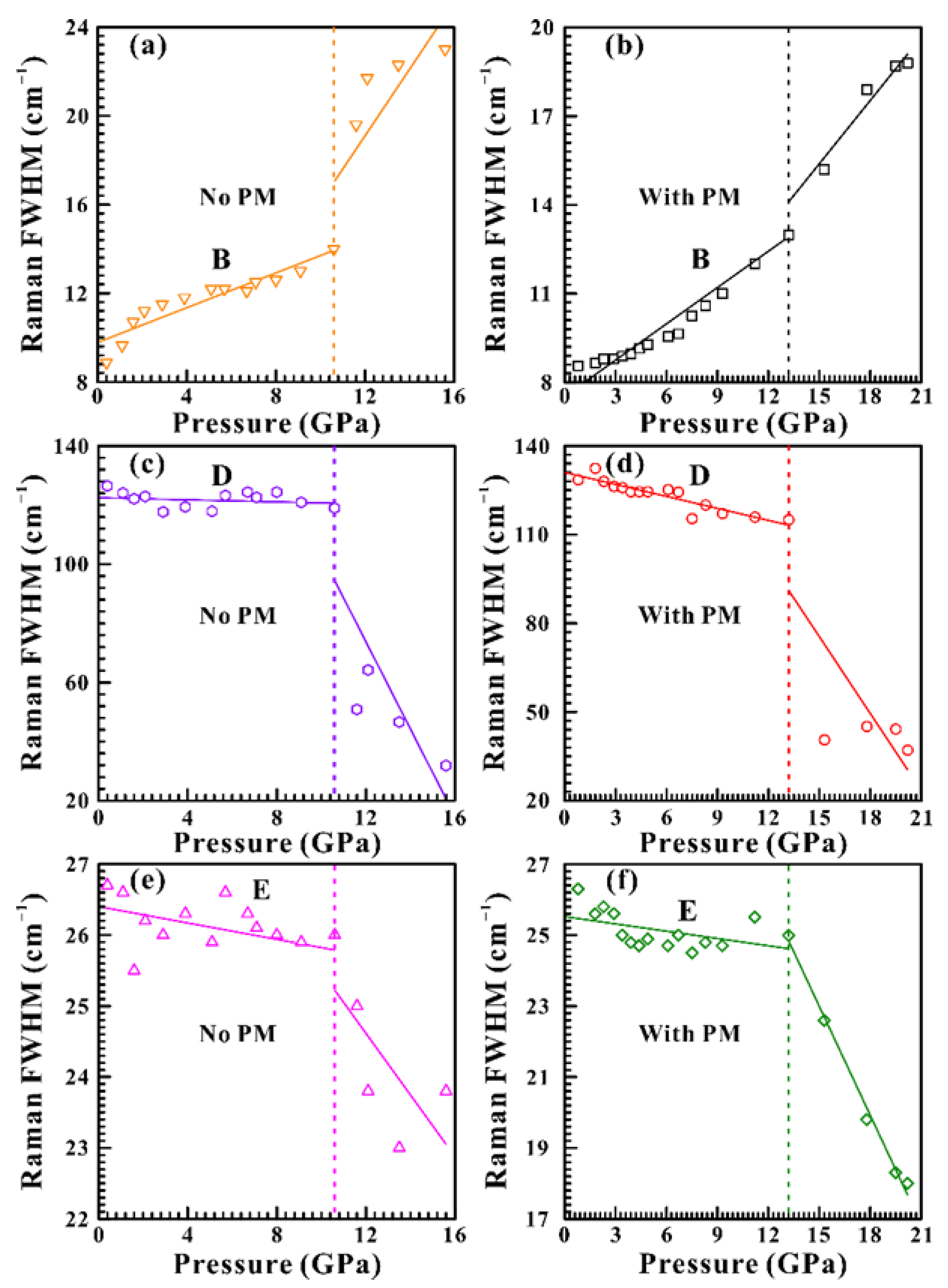
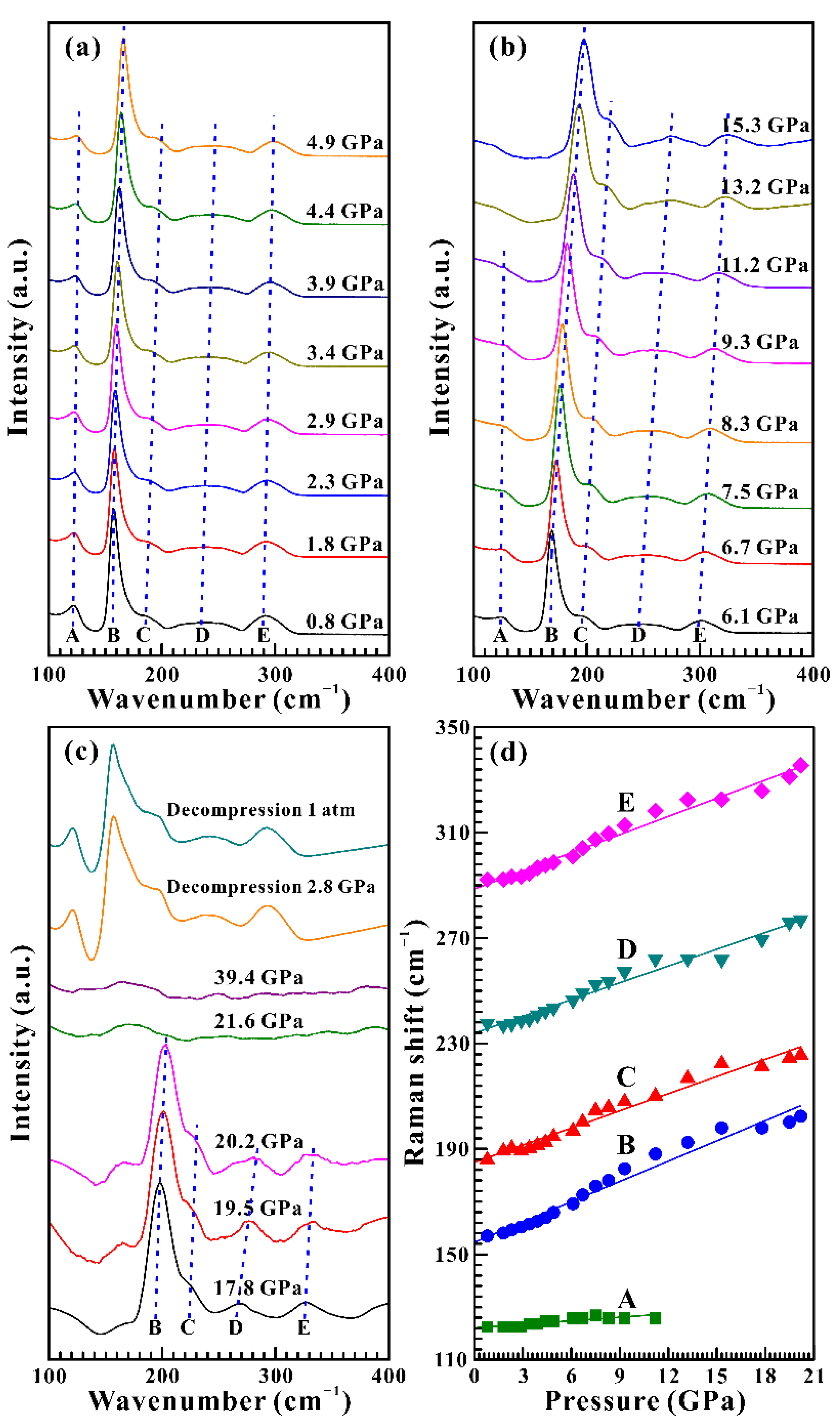
3.1. High-Pressure Raman Spectra Results

High-pressure Raman spectroscopy was performed to investigate the structural and vibrational properties of Ga2Se3 under different hydrostatic environments. Figure 2 and Figure 3a,c,e display the variation of Raman peaks, Raman shifts, and Raman FWHMs for Ga2Se3 with pressure in the range of 0.4–39.5 GPa and at room temperature under non-hydrostatic conditions. The corresponding results of the pressure-dependent Raman shifts and Raman FWHMs for Ga2Se3 are listed in Table 1 and Table 2, respectively. From Figure 2a, five characteristic Raman-active peaks at 121.3, 157.0, 185.9, 237.6, and 291.1 cm−1 were observed within the wavenumber range of 100–400 cm−1 at the pressure of 0.4 GPa, which could be identified as the A, B, C, D, and E modes, respectively. All of these acquired Raman peaks agreed well with prior studies [3,20,21,22].
As shown in Figure 2a–c, with increasing pressure, the B, C, D, and E modes of Ga2Se3 continuously shifted towards higher wavenumbers up to 15.6 GPa, and no anomaly was found in the pressure-dependent Raman shifts. Meanwhile, the A mode also exhibited a blue shift with a relatively slow speed of 0.54 cm−1 GPa−1, whereas its Raman peak intensity weakened significantly as the pressure increased. When the pressure reached 10.6 GPa, the A mode disappeared, which might be indicative of the phase transition from the zinc-blende to NaCl-type structure in Ga2Se3. Additionally, by analyzing the pressure-dependent FWHMs of three stronger Raman peaks at 157.0, 237.6, and 291.1 cm−1, two pressure regions of 0.4–10.6 GPa and 10.6–15.6 GPa could be distinguished based on various pressure-dependent Raman FWHM slopes. More specifically, the FWHM of the B mode increased slightly with the rise of pressure at a rate of 0.39 cm−1 GPa−1 below 10.6 GPa, while a greater slope of 1.51 cm−1 GPa−1 was acquired within the pressure range of 10.6–15.6 GPa. In regard to the D and E modes, two relatively small pressure-dependent Raman FWHM slopes of –0.18 cm−1 GPa−1 and –0.031 cm−1 GPa−1 were detected within the pressure range of 0.4–10.6 GPa, respectively. However, when the pressure exceeded 10.6 GPa, the FWHMs of the D and E modes decreased rapidly with increasing pressure at the separate rates of –13.87 cm−1 GPa−1 and –0.43 cm−1 GPa−1. According to the pressure-dependent Raman FWHM results, an apparent discontinuity was found at 10.6 GPa, which provided robust evidence for the occurrence of phase transition from the zinc-blende to NaCl-type structure in Ga2Se3. Further compression to 17.8 GPa, the Raman peaks of the sample disappeared completely, and only one broad hump was observed up to the highest pressure of 39.5 GPa. Upon decompression from 39.5 GPa to 3.9 GPa, the Raman spectra of the sample remained featureless. As the pressure was continuously reduced to 3.1 GPa, five representative Raman peaks of Ga2Se3 reappeared at the positions of 125.8, 172.6, 205.7, 252.9, and 304.1 cm−1, and they moved towards lower wavenumbers with decreasing pressure. Further decompressing to ambient conditions, all of these Raman peaks of Ga2Se3 were recoverable to their original state. Therefore, the phase transformation of the zinc-blende to a NaCl-type structure in Ga2Se3 was reversible, but there existed a large pressure hysteresis effect, which possibly resulted from the greater kinetic barrier of the structural transition during decompression.
Under hydrostatic conditions, the pressure-dependent Raman peaks, Raman shifts, and Raman FWHMs for Ga2Se3 were similar to those observed under non-hydrostatic conditions, as displayed in Figure 3b,d,f and Figure 4. However, the phase transition was detected at the higher pressure point of 13.2 GPa compared with those under non-hydrostatic conditions at 10.6 GPa. The discrepancy in the pressure point of structural transition under different hydrostatic environments was probably attributed to the deviatoric stress. Under non-hydrostatic conditions, the deviatoric stress in the sample chamber facilitated the occurrence of phase transition. However, the existence of the pressure medium played an important role in weakening the deviatoric stress inside the sample chamber and thus delaying the occurrence of phase transition. A similar phenomenon has also been reported in our previously studied A2B3-type metal dichalcogenides (e.g., As2Te3, Ga2S3 et al.) [9,13] and sphalerite-structure compounds (e.g., GaP, ZnSe et al.) [18,19].

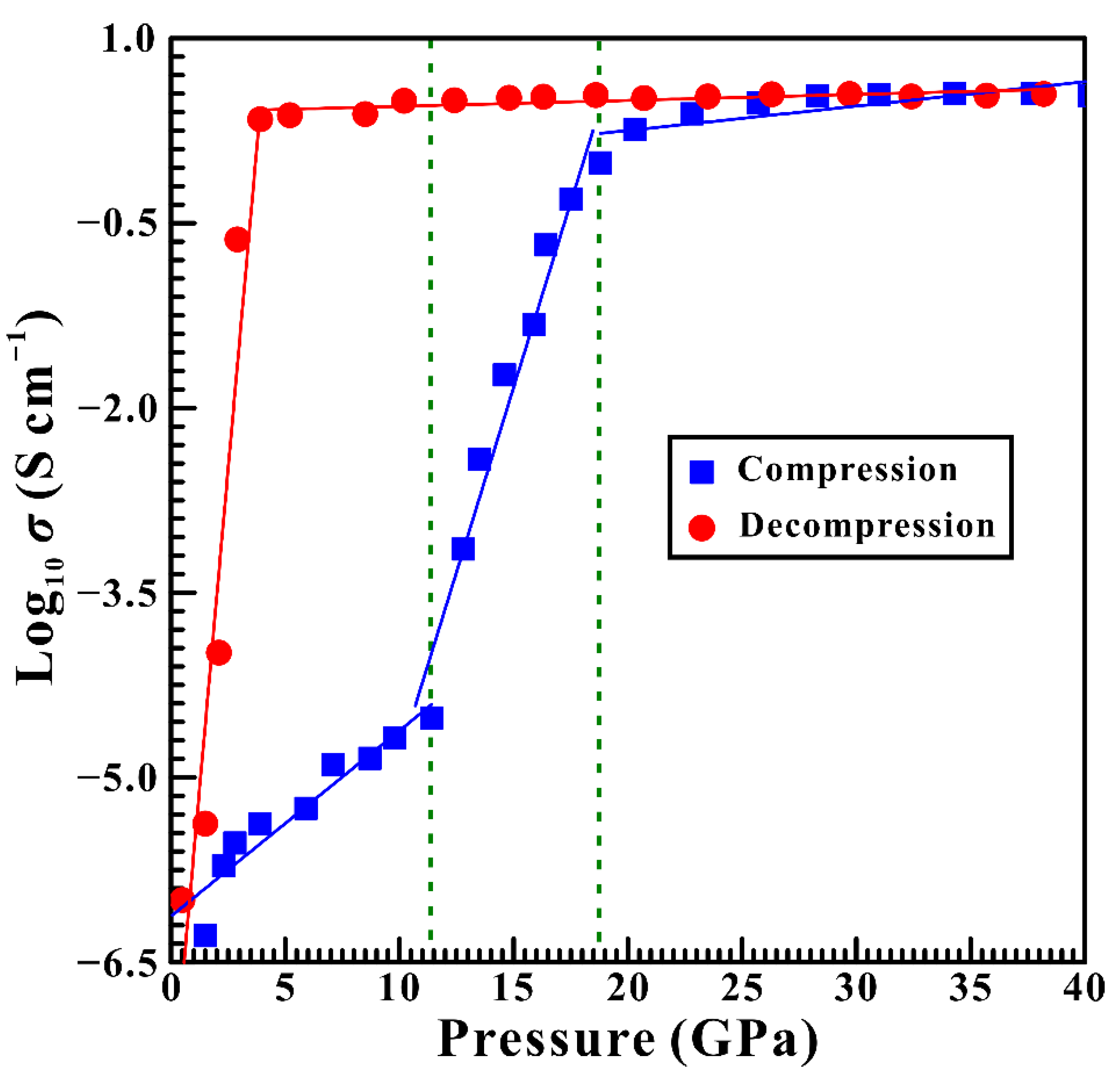
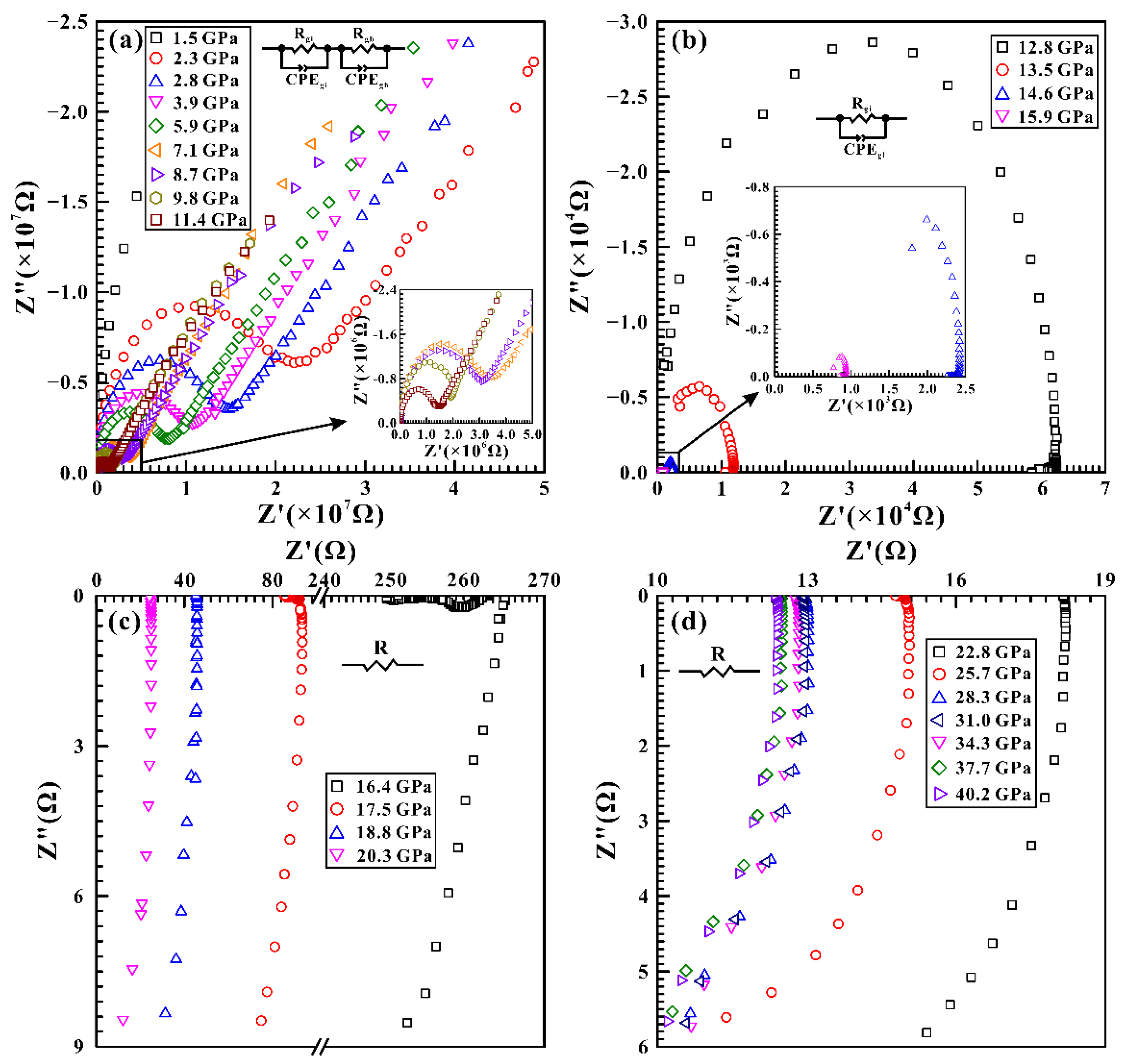
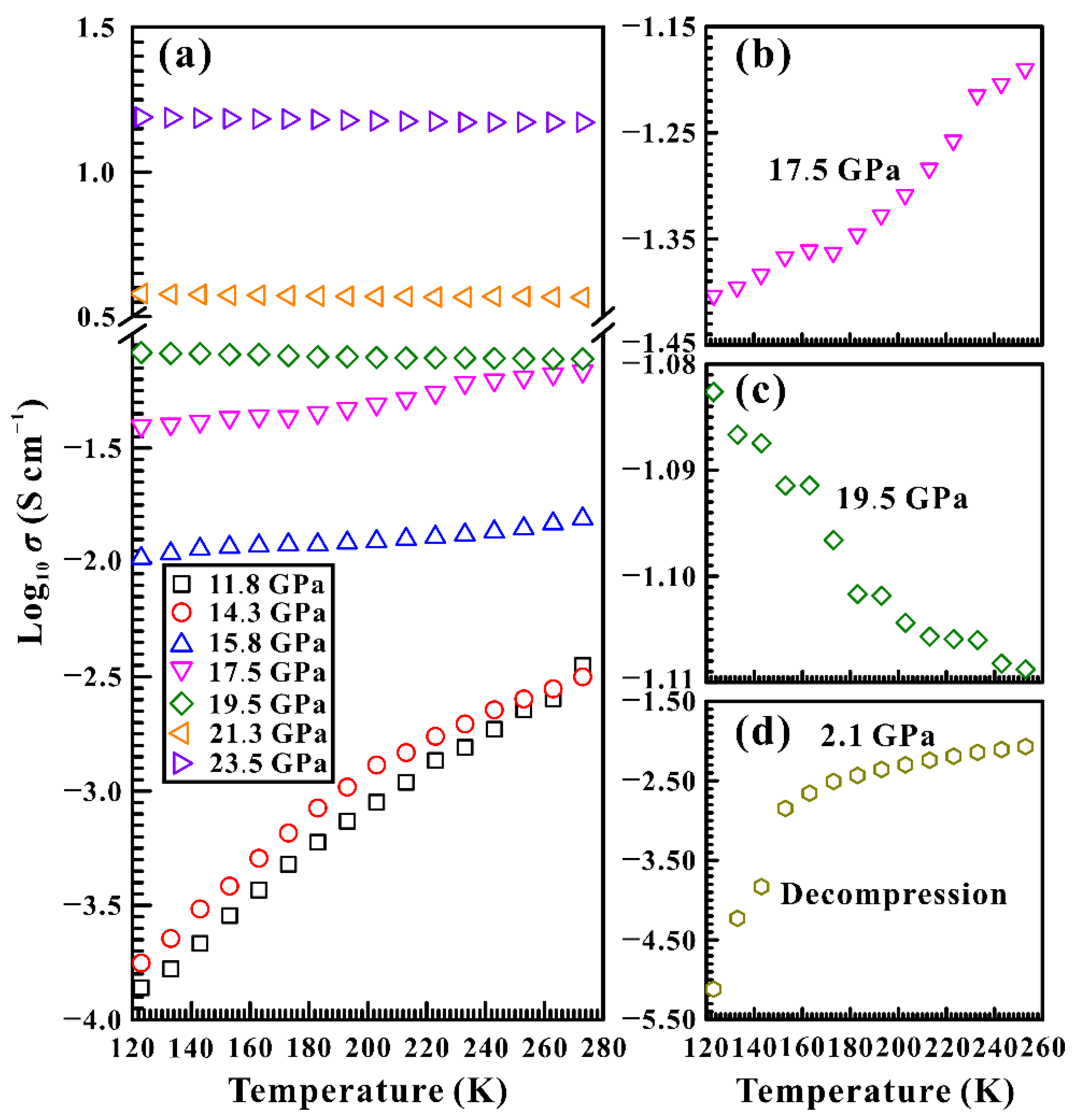
3.2. High-Pressure Electrical Conductivity Results

Typical complex impedance spectra for Ga2Se3 under the conditions of 1.5–40.2 GPa and room temperature are plotted in Figure 5. Within the pressure range of 1.5–11.4 GPa, the impedance spectra consisted of two components: a semicircle within the high-frequency region (~103–107 Hz), which stands for the grain interior contribution of the sample, and the tail in the low-frequency regime (10−1–~103 Hz) that represents the grain boundary contribution of the sample. When the pressure was enhanced above 11.4 GPa, the low-frequency tail disappeared, and only the high-frequency semicircular arc was observed. Each of the impedance semicircular arcs within the pressure range of 1.5–15.9 GPa could be simulated by an appropriate equivalent circuit made up of a parallel resistance (R) and a constant phase element (CPE) using the complex non-linear least-squares fitting routine in Zview software. On further increasing the pressure above 15.9 GPa, the impedance spectra appeared in the fourth quadrant, which can be fitted by the simple resistance (R). The electrical conductivity of the sample was calculated using the following formula:
σ = D/SR
where D is the distance between the electrodes (cm), S is the cross-section area of the electrode (cm2), R is the sample resistance (Ω), and σ is the electrical conductivity of the sample (S cm−1). Figure 6 illustrates the logarithmic electrical conductivities of Ga2Se3 as a function of pressure in the processes of compression and decompression. In the pressure range of 1.5–11.4 GPa, the electrical conductivity of the sample increased slowly with the rise of the pressure at a rate of 0.15 S cm−1 GPa−1. However, a drastic increase in electrical conductivity by about four orders of magnitude was observed as the pressure was enhanced from 11.4 GPa to 18.8 GPa. The obvious discontinuity in electrical conductivity at 11.4 GPa proved the occurrence of a phase transition from the zinc-blende to NaCl-type structure in Ga2Se3, which coincided with our above-mentioned Raman scattering results under non-hydrostatic conditions. On further increasing the pressure from 18.8 GPa to 40.2 GPa, the electrical conductivity of the sample was slightly enhanced within the range of 0.97–3.58 S cm−1. Such high electrical conductivity values indicate the occurrence of the semiconductor-to-metal phase transition. Upon decompression, the electrical conductivity of the sample remained relatively stable above 3.9 GPa but decreased dramatically by about six orders of magnitude in the pressure range of 3.9–0.5 GPa. The apparent inflection point in the pressure-dependent electrical conductivity at 3.9 GPa agreed well with our high-pressure Raman scattering results under non-hydrostatic conditions and revealed that the phase transformation of the zinc-blende to the NaCl-type structure in Ga2Se3 was reversible upon decompression. When further decompressed to 0.5 GPa, the electrical conductivity of the sample returned to its original order of magnitude, which suggests that the metallization of Ga2Se3 is reversible upon decompression.
To verify whether Ga2Se3 undergoes a semiconductor-to-metal phase transition, a series of temperature-variable electrical conductivity measurements were performed at some representative pressure points of 11.8, 14.3, 15.8, 17.5, 19.5, 21.3, and 23.5 GPa. As usual, the semiconductor displayed a positive temperature-dependent electrical conductivity relation. Conversely, the electrical conductivity of metal decreased with the rise of temperature [9,10,13]. It can be seen clearly from Figure 7 that the electrical conductivity of Ga2Se3 enhanced with increasing temperature up to 17.5 GPa, which reflects that the sample is a semiconductor. However, negative temperature-dependent electrical conductivity relations were observed above 19.5 GPa, which implies metallic behavior. In addition, we also conducted the temperature-dependent electrical conductivity measurement for the recovered Ga2Se3 sample at 2.1 GPa, as illustrated in Figure 7d. A positive temperature-dependent electrical conductivity correlation was found, which demonstrates that the recovered Ga2Se3 sample behaves as typical semiconducting behavior. Thus, our variable-temperature electrical conductivity experiments under high pressure confirm the occurrence of metallization in Ga2Se3 at 18.8 GPa and the recovered Ga2Se3 sample is a typical semiconductor.
Microscopic structural characterizations and morphology observations for the initial sample and the recovered samples decompressed under both non-hydrostatic and hydrostatic environments were investigated by high-resolution transmission electron microscopy (HRTEM) and atomic force microscopy (AFM). Figure 8 shows cross-section HRTEM images and their corresponding fast Fourier transform (FFT) patterns for the initial sample, as well as the recovered samples decompressed from 39.4 GPa under non-hydrostatic conditions and decompressed from 39.6 GPa under hydrostatic conditions. The initial sample displayed clear lattice fringes with the interplanar spacing of ~0.32 nm, which corresponded to the (111) oriented crystal plane of the cubic structured Ga2Se3. It is well known that the (111) plane is the most close-packed and frequently observed facet for the sphalerite-structure compounds [3,22]. Moreover, the interplanar spacing distances (~0.31 nm) for the recovered samples decompressed under both non-hydrostatic and hydrostatic environments were almost the same as the initial sample, which further verified that the recovered samples are cubic Ga2Se3. Additionally, all of these FFT patterns of HRTEM images for the initial sample and the recovered samples exhibited electronic diffraction rings comprising of a series of bright diffraction spots. However, the arrangement of the diffraction spots in Figure 8b,f are more regular than that in Figure 8d, which implies that the initial sample and the recovered sample under hydrostatic conditions were of better crystalline quality. The well-preserved crystalline structure of the recovered sample under hydrostatic conditions might be associated with the protective effect of the pressure medium.
Figure 9 displays the typical three-dimensional atomic force microscopy (AFM) images for the initial sample and the recovered samples. All of these images present the discernible layered morphology in the selected region, which confirms that the phase transition of the zinc-blende to NaCl-type structure in Ga2Se3 is reversible. In addition, the maximum height of the initial sample was approximately 232.9 nm in the chosen square region, and whereas, relatively smaller sample heights of 36.7 nm and 69.8 nm were obtained for the recovered samples under non-hydrostatic and hydrostatic environments, respectively. The discrepancy in the sample height possibly arose from the different sample grain sizes.

4. Conclusions

The high-pressure structural, vibrational, and electrical transport properties for Ga2Se3 were comprehensively studied in a diamond anvil cell up to 40.2 GPa under different hydrostatic environments using Raman spectroscopy, AC impedance spectroscopy, high-resolution transmission electron microscopy, and atomic force microscopy. Under non-hydrostatic conditions, the zinc-blende to NaCl-type structural transition in Ga2Se3 was detected at 10.6 GPa, followed by a semiconductor-to-metal phase transition at 18.8 GPa. However, the same structural transition was delayed by roughly 3.0 GPa under hydrostatic conditions, which was ascribed to the protective effect of the pressure medium. Upon decompression, the recoverable Raman spectrum and electrical conductivity values showed that the structural transition and metallization for Ga2Se3 were reversible, which were confirmed by our HRTEM and AFM results.

Author Contributions

Conceptualization, L.D., H.H. and M.H.; methodology, L.D. and M.H.; software, L.D. and H.H.; validation, M.H. and X.Z.; formal analysis, L.D. and M.H.; investigation, L.D.; resources, L.D. and H.H.; data curation, M.H. and X.Z.; writing—original draft preparation, L.D., H.H., M.H. and X.Z.; writing—review and editing, L.D.; visualization, M.H.; supervision, L.D. and H.H.; project administration, L.D.; funding acquisition, L.D. and H.H. All authors have read and agreed to the published version of the manuscript.

Funding

This research was funded by the NSF of China (grant numbers 42072055, 41774099 and 41772042), the Youth Innovation Promotion Association of CAS (grant number 2019390), the Special Fund of the West Light Foundation of CAS, as well as the Special Fund from Shandong Provincial Key Laboratory of Water and Soil Conservation and Environmental Protection.

Institutional Review Board Statement

Not applicable.

Informed Consent Statement

Not applicable.

Data Availability Statement

All data that support the findings of this study are available from the corresponding author upon reasonable request.

Acknowledgments

The authors acknowledge the technical support of the in situ high-pressure Raman scattering measurements provided by Heping Li in the Key Laboratory of High-temperature and High-Pressure Study of the Earth’s Interior, Institute of Geochemistry, Chinese Academy of Sciences.

Conflicts of Interest

The authors declare no conflict of interest.

References

  1. Gurevich, Y.G.; Koshkin, V.M.; Volovichev, I.N. The heterocontact of two intrinsic semiconductors and radiation-stable electronics. Solid-State Electron. 1995, 38, 235–242. [Google Scholar] [CrossRef]
  2. Guler, I.; Isik, M.; Gasanly, N.M.; Gasanova, L.G.; Babayeva, R.F. Structural and optical properties of Ga2Se3 crystals by spectroscopic ellipsometry. J. Electron. Mater. 2019, 48, 2418–2422. [Google Scholar] [CrossRef]
  3. Ho, C.H. Ga2Se3 defect semiconductors: The study of direct band edge and optical properties. ACS Omega 2020, 5, 18527–18534. [Google Scholar] [CrossRef] [PubMed]
  4. Guo, S.P.; Cheng, X.Y.; Sun, Z.D.; Chi, Y.; Liu, B.W.; Jiang, X.M.; Li, S.F.; Xue, H.G.; Deng, S.Q.; Duppel, V.; et al. Large SHG effect and high LIDT observed coexisting in gallium selenide: A simple but perfect case. Angew. Chem. Int. Ed. 2019, 58, 8087–8091. [Google Scholar] [CrossRef] [PubMed]
  5. Savchenko, K.V. X-ray-induced conductivity in gallium sesqui-selenide. Tech. Phys. Lett. 2008, 34, 964–966. [Google Scholar] [CrossRef]
  6. Yitamben, E.N.; Lovejoy, T.C.; Pakhomov, A.B.; Heald, S.M.; Negusse, E.; Arena, D.; Ohuchi, F.S.; Olmstead, M.A. Correlation between morphology, chemical environment, and ferromagnetism in the intrinsic-vacancy dilute magnetic semiconductor Cr-doped Ga2Se3/Si (001). Phys. Rev. B 2011, 83, 045203. [Google Scholar] [CrossRef] [Green Version]
  7. Ding, J.J.; Zhou, Y.N.; Cui, Y.H.; Fu, Z.W. Ga2Se3 thin film as a negative electrode material for lithium-ion batteries. ECS Electrochem. Lett. 2012, 1, A7–A9. [Google Scholar] [CrossRef]
  8. Jin, H.; Zhang, H.J.; Li, J.W.; Wang, T.; Wan, L.H.; Guo, H.; Wei, Y.D. Data-driven systematic search of promising photocatalysts for water splitting under visible light. J. Phys. Chem. Lett. 2019, 10, 5211–5218. [Google Scholar] [CrossRef]
  9. Dai, L.D.; Zhuang, Y.K.; Li, H.P.; Wu, L.; Hu, H.Y.; Liu, K.X.; Yang, L.F.; Pu, C. Pressure-induced irreversible amorphization and metallization with a structural phase transition in arsenic telluride. J. Mater. Chem. C 2017, 5, 12157–12162. [Google Scholar] [CrossRef]
  10. Dai, L.D.; Liu, K.X.; Li, H.P.; Wu, L.; Hu, H.Y.; Zhuang, Y.K.; Yang, L.F.; Pu, C.; Liu, P.F. Pressure-induced irreversible metallization accompanying the phase transitions in Sb2S3. Phys. Rev. B 2018, 97, 024103. [Google Scholar] [CrossRef]
  11. Liu, K.X.; Dai, L.D.; Li, H.P.; Hu, H.Y.; Yang, L.F.; Pu, C.; Hong, M.L.; Liu, P.F. Phase transition and metallization of orpiment by Raman spectroscopy, electrical conductivity and theoretical calculation under high pressure. Materials 2019, 12, 784. [Google Scholar] [CrossRef] [PubMed] [Green Version]
  12. Liu, K.X.; Dai, L.D.; Li, H.P.; Hu, H.Y.; Yang, L.F.; Pu, C.; Hong, M.L. Evidences for phase transition and metallization in β-In2S3 at high pressure. Chem. Phys. 2019, 524, 63–69. [Google Scholar] [CrossRef]
  13. Yang, L.F.; Jiang, J.J.; Dai, L.D.; Hu, H.Y.; Hong, M.L.; Zhang, X.Y.; Li, H.P.; Liu, P.F. High-pressure structural phase transition and metallization in Ga2S3 under non-hydrostatic and hydrostatic conditions up to 36.4 GPa. J. Mater. Chem. C 2021, 9, 2912–2918. [Google Scholar] [CrossRef]
  14. Savchenko, K.V.; Shchennikov, V.V. A phase transition in Ga2Se3 under high pressure. Can. J. Phys. 1994, 72, 681–682. [Google Scholar] [CrossRef]
  15. Takumi, M.; Hirata, A.; Ueda, T.; Koshio, Y.; Nishimura, H.; Nagata, K. Structural phase transitions of Ga2Se3 and GaSe under high pressure. Phys. Status Solidi (B) 2001, 223, 423–426. [Google Scholar] [CrossRef]
  16. Zhao, J.G.; Yang, L.X. Structure evolutions and metallic transitions in In2Se3 under high pressure. J. Phys. Chem. C 2014, 118, 5445–5452. [Google Scholar] [CrossRef]
  17. Shchennikov, V.V.; Savchenko, K.V.; Popova, S.V. Electrical properties of the high-pressure phases of gallium and indium tellurides. Phys. Solid State 2000, 42, 1036–1040. [Google Scholar] [CrossRef]
  18. Dai, L.D.; Pu, C.; Li, H.P.; Hu, H.Y.; Liu, K.X.; Yang, L.F.; Hong, M.L. Characterization of metallization and amorphization for GaP under different hydrostatic environments in diamond anvil cell up to 40.0 GPa. Rev. Sci. Instrum. 2019, 90, 066103. [Google Scholar] [CrossRef]
  19. Pu, C.; Dai, L.D.; Li, H.P.; Hu, H.Y.; Liu, K.X.; Yang, L.F.; Hong, M.L. Pressure-induced phase transitions of ZnSe under different pressure environments. AIP Adv. 2019, 9, 025004. [Google Scholar] [CrossRef] [Green Version]
  20. Finkman, E.; Tauc, J.; Kershaw, R.; Wold, A. Lattice dynamics of tetrahedrally bonded semiconductors containing ordered vacant sites. Phys. Rev. B 1975, 11, 3785–3794. [Google Scholar] [CrossRef]
  21. Yamada, A.; Kojima, N.; Takahashi, K.; Okamoto, T.; Konagai, M. Raman study of epitaxial Ga2Se3 films grown by molecular beam epitaxy. Jpn. J. Appl. Phys. 1992, 31, L186–L188. [Google Scholar] [CrossRef]
  22. Ho, C.H.; Lai, X.R.; Chuang, C.A.; Kuo, W.L.; Tiong, K.K. The study of optical properties of III2–VI3 defect semiconductor group compounds Ga2S3, Ga2Se3, In2S3, and In2Se3. Adv. Photonics Res. 2021, 2, 2000110. [Google Scholar] [CrossRef]
Figure 1. X-ray diffraction (XRD) pattern of the initial Ga2Se3 sample. Red vertical lines present the standardized diffraction peak positions of Ga2Se3. Inset: Optical microscope image and the calculated lattice parameters for the initial sample.
Crystals 11 00746 g001
Figure 2. (ac) Raman spectra of Ga2Se3 at the pressure range of 0.4–39.5 GPa during compression, and the Raman spectra at the pressure points of 3.1 GPa and 1atm during decompression; (d) Pressure dependence of Raman shifts for Ga2Se3 under non-hydrostatic conditions. In here, the A, B, C, D and E modes referred to the Raman-active peaks at 121.3, 157.0, 185.9, 237.6, and 291.1 cm−1 obtained at 0.4 GPa, respectively.
Crystals 11 00746 g002
Figure 3. Pressure dependence of the Raman full width at half maximum (FWHMs) for Ga2Se3 (a,c,e) under non-hydrostatic conditions; (b,d,f) under hydrostatic conditions, respectively. Here, PM represents the pressure medium. The B, D and E modes represent the Raman peaks at 157.0, 237.6 and 291.1 cm−1 obtained at 0.4 GPa under non-hydrostatic conditions and at 157.0, 237.6 and 292.2 cm−1 obtained at 0.8 GPa under hydrostatic conditions, respectively.
Crystals 11 00746 g003
Figure 4. (ac) Raman spectra of Ga2Se3 at the pressure range of 0.8–39.4 GPa during compression, and the Raman spectra at the pressure points of 2.8 GPa and 1atm during decompression; (d) Pressure-dependent Raman shifts for Ga2Se3 under hydrostatic conditions. In here, the A, B, C, D and E modes stand for the Raman peaks at 122.5, 157.0, 185.9, 237.6, and 292.2 cm−1 acquired at 0.8 GPa, respectively.
Crystals 11 00746 g004
Figure 5. Complex impedance spectra of Ga2Se3 measured under the conditions of room temperature and (a) 1.5–11.4 GPa; (b) 12.8–15.9 GPa; (c) 16.4–20.3 GPa; and (d) 22.8–40.2 GPa, respectively. Z’ and Z" are the real and imaginary parts of the complex impedance, respectively. An appropriate equivalent circuit of a single R/CPE in parallel is employed to fit the high-frequency semicircle arc and the low-frequency tail. Here, Rgi and Rgb are the resistances of the grain interior and grain boundary, respectively. CPEgi and CPEgb stand for the constant phase elements of the grain interior and grain boundary, respectively. The impedance spectra appearing in the fourth quadrant can be modeled by the simple resistance (R).
Crystals 11 00746 g005
Figure 6. The logarithm of electrical conductivity of Ga2Se3 as a function of pressure at atmospheric temperature under both compression and decompression.
Crystals 11 00746 g006
Figure 7. (a) The temperature—dependent logarithmic electrical conductivity for Ga2Se3 at some representative pressure points of 11.8, 14.3, 15.8, 17.5, 19.5, 21.3, and 23.5 GPa; (b)The semiconducting behavior of Ga2Se3 at 17.5 GPa; (c) The metallic state of the sample at 19.5 GPa; (d) Typical semiconducting character for the recovered Ga2Se3 sample decompressed to 2.1 GPa.
Crystals 11 00746 g007
Figure 8. High-resolution transmission electron microscopy (HRTEM) images and their corresponding fast Fourier transform (FFT) patterns for Ga2Se3. (a,b): The images of the initial sample; (c,d): The images of the recovered sample decompressed from 39.4 GPa under non-hydrostatic conditions; (e,f): The images for the recovered sample decompressed from 39.6 GPa under hydrostatic conditions. Here, PM is the pressure medium.
Crystals 11 00746 g008
Figure 9. Three-dimensional atomic force microscopy (AFM) images of Ga2Se3. (a) The image of the initial sample; (b,c): The images for the recovered samples decompressed from 39.4 GPa under non-hydrostatic conditions and decompressed from 39.6 GPa under hydrostatic conditions, respectively. Here, PM stands for the pressure medium.
Crystals 11 00746 g009
Table 1. Pressure-dependent Raman shift (dω/dP; cm−1 GPa−1) for Ga2Se3 under non-hydrostatic and hydrostatic environments. Here, ω and P are the Raman frequency and pressure, respectively. The listed ω values are obtained at 0.4 GPa under non-hydrostatic conditions and at 0.8 GPa under hydrostatic conditions, respectively.
Pressure
Condition
Pressure (GPa)ω (cm−1)dω/dP
(cm−1 GPa−1)
ω (cm−1)dω/dP
(cm−1 GPa−1)
Non-hydrostatic0.4–15.6121.3 (A)0.54157.0 (B)2.51
185.9 (C)1.89237.6 (D)2.03
291.1 (E)2.34
Hydrostatic0.8–20.2122.5 (A)0.45157.0 (B)2.56
185.9 (C)2.17237.6 (D)2.12
292.2 (E)2.30
Table 2. Pressure dependence of Raman FWHM (dF/dP; cm−1 GPa−1) for Ga2Se3 under non-hydrostatic and hydrostatic environments. Here, ω, F, and P are the Raman frequency, Raman FWHM, and pressure, respectively. The listed ω values are obtained at 0.4 GPa within the pressure range of 0.4–10.6 GPa and at 10.6 GPa within the pressure range of 10.6–15.6 GPa under non-hydrostatic conditions, respectively. The listed ω values are acquired at 0.8 GPa within the pressure range of 0.8–13.2 GPa and at 13.2 GPa within the pressure range of 13.2–20.2 GPa under hydrostatic conditions, respectively.
Pressure ConditionPressure (GPa)ω
(cm−1)
dF/dP
(cm−1 GPa−1)
ω
(cm−1)
dF/dP
(cm−1 GPa−1)
ω
(cm−1)
dF/dP
(cm−1 GPa−1)
Non-hydrostatic0.4–10.6157.0 (B)0.39237.6 (D)–0.18291.1 (E)–0.031
10.6–15.6183.7 (B)1.51256.2 (D)–13.87313.9 (E)–0.43
Hydrostatic0.8–13.2157.0 (B)0.36237.6 (D)–1.34292.2 (E)–0.068
13.2–20.2192.5 (B)0.87262.1 (D)–8.67322.5 (E)–1.02
Publisher’s Note: MDPI stays neutral with regard to jurisdictional claims in published maps and institutional affiliations.

