Article

Xenon Plasma Focused Ion Beam Milling for Obtaining Soft X-ray Transparent Samples

1
Paul Scherrer Institut (PSI), 5232 Villigen, Switzerland
2
Laboratory for Mesoscopic Systems, Department of Materials, ETH Zurich, 8093 Zurich, Switzerland
3
Scientific Center for Optical and Electron Microscopy, ETH Zurich, 8093 Zurich, Switzerland
4
INNOVENT e.V. Technologieentwicklung Jena, 07745 Jena, Germany
5
Helmholtz-Zentrum Berlin, 14109 Berlin, Germany
6
Laboratory for Magnetism and Interface Physics, Department of Materials, ETH Zurich, 8093 Zurich, Switzerland
7
Max Planck Institute for Intelligent Systems, 70569 Stuttgart, Germany
*
Authors to whom correspondence should be addressed.
Crystals 2021, 11(5), 546; https://doi.org/10.3390/cryst11050546
Submission received: 25 March 2021 / Revised: 2 May 2021 / Accepted: 3 May 2021 / Published: 14 May 2021
(This article belongs to the Special Issue Advanced Imaging Methods)

Abstract

:
We employ xenon (Xe) plasma focused ion beam (PFIB) milling to obtain soft X-ray transparent windows out of bulk samples. The use of a Xe PFIB allows for the milling of thin windows (several 100 nm thick) with areas of the order of 100 µm × 100 µm into bulk substrates. In addition, we present an approach to empirically determine the transmission level of such windows during fabrication by correlating their electron and soft X-ray transparencies. We perform scanning transmission X-ray microscopy (STXM) imaging on a sample obtained by Xe PFIB milling to demonstrate the conceptual feasibility of the technique. Our thinning approach provides a fast and simplified method for facilitating soft X-ray transmission measurements of epitaxial samples and it can be applied to a variety of different sample systems and substrates that are otherwise not accessible.

1. Introduction

X-rays from synchrotron light sources, with their high brilliance and tunable energy, have become an indispensable tool for a variety of research fields. Within the broad X-ray spectrum, soft X-rays with energies up to ~2 keV cover the central resonant electron transitions of a wide range of elements. This key feature allows for an element-specific analysis of materials while further providing information on both their magnetic and chemical states [1]. In addition, soft X-ray microscopy techniques typically offer higher spatial resolutions than visible light microscopy techniques as a result of the up to two orders of magnitude shorter wavelengths of soft X-rays [2].
On this background, X-ray transmission experiments, i.e., the detection of photons transmitted through the sample, are of particular interest as they give access to the full sample structure, including buried layers. Moreover, photon-in photon-out measurement schemes allow for a simple application of electric and magnetic fields, not compromising the detection as it can be the case for electrons. However, a disadvantage of such transmission measurements is the necessity to have X-ray transparent samples. This requirement can be challenging as the attenuation length in the soft X-ray regime is of the order of tens to several hundreds of nanometers, depending on the sample material and X-ray energy [3]. For that reason, samples are typically grown on X-ray transparent amorphous Si3N4 membranes of ~100 nm thickness. However, this approach excludes single-crystalline and other thin film systems that need to be grown on specific substrates, for example certain antiferromagnets [4,5], semiconductors [6] or perovskites [7,8].
To overcome the issue of nontransparent substrates, for some material systems selective chemical etching can be applied to specifically remove parts of the sample [9,10]. Another possibility is to extract a lamella out of a thin film or bulk substrate and then place it on a membrane for measurements [11,12]. The disadvantage of this processing is that only a small, confined element and not a full film can be studied.
Another approach to fabricate soft X-ray transparent samples is to use focused gallium ion beam (Ga FIB) milling in combination with mechanical grinding to remove substrate material until the samples are transparent in the soft X-ray regime [13,14,15,16,17,18]. While this technique marks an important milestone for X-ray transmission experiments, it is at the same time severely limited by the relatively low milling speed of the Ga FIBs used. The pre-processing for the Ga FIB milling typically involves mechanical planar grinding of the whole sample to a thickness of below 100 µm, followed by a local thickness reduction to several micrometers with a dimple grinder. At the center of this emerging dimple, the remaining material is then removed with a Ga FIB until a local window with a thickness of below 1 µm is fabricated.
Here, we show that by the use of a xenon (Xe) Plasma FIB (PFIB), for which more than 10 times faster milling speeds are possible [19], we can simplify and extend the Ga FIB window milling technique described above. As a result of these faster milling speeds, the samples may have a thickness prior to the FIB step from around 50 µm to more than 100 µm, depending on the actual milling properties of the material. Therefore, the dimple-grinding step can always be omitted and we can instead work with a plane substrate, and for sufficiently thin substrates even the initial grinding step would not be necessary anymore. Moreover, we present an approach to indirectly determine the soft X-ray transparency of the milled windows during the PFIB fabrication process by making use of the scanning electron microscope (SEM) column the PFIB two-beam system is equipped with. We illustrate the feasibility of our method by scanning transmission X-ray microscopy (STXM) measurements.

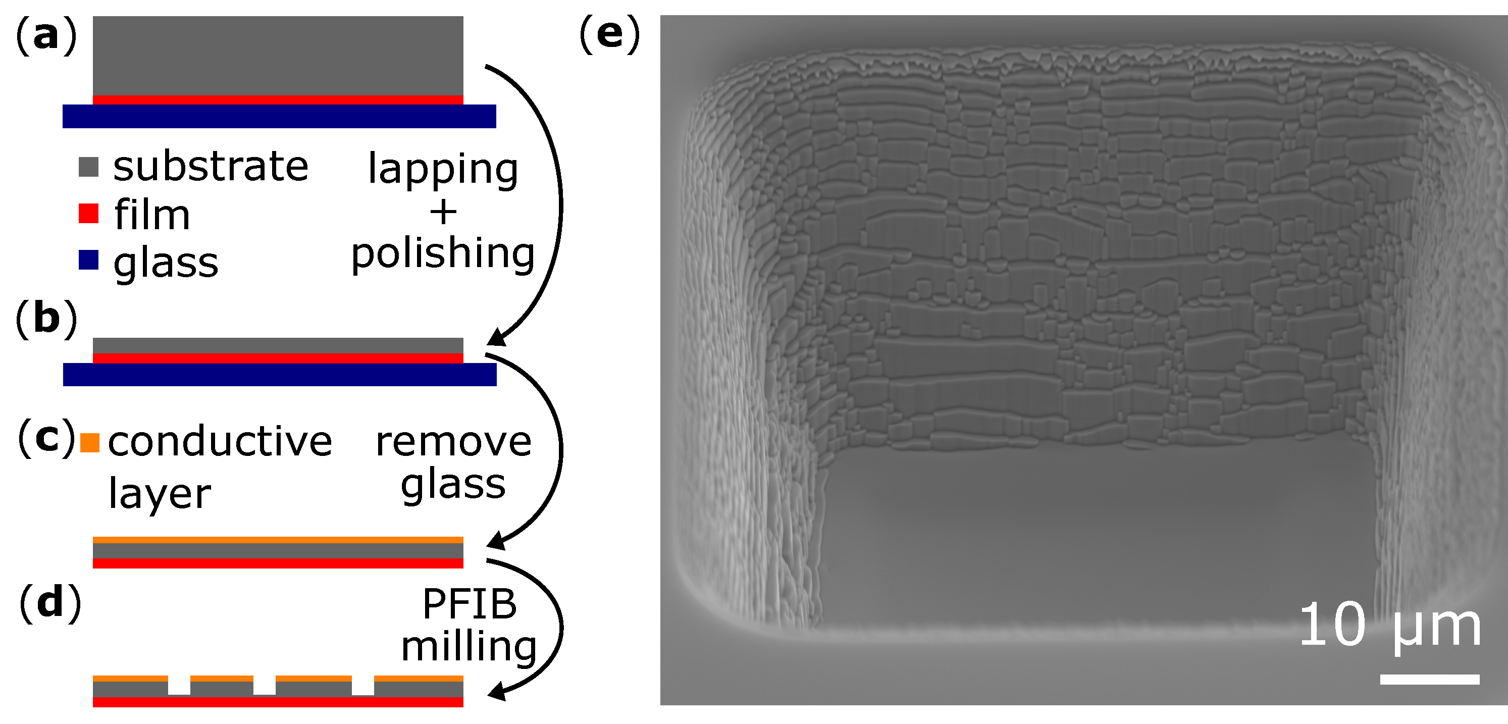
2. Materials and Methods

The standard sample system considered here comprises a thin film grown on a bulk substrate. Nevertheless, it is possible to process bulk samples as well, with the moderate disadvantage that the sample will be directly affected by the Xe+ ions. For processing with the Xe PFIB, we found that the substrate should typically have a thickness between 50 µm and 120 µm. Thinner samples are fragile and need additional support for processing, while for thicker ones milling problems such as redeposition become an issue. The actual thickness can be chosen depending on the milling speed of the specific material. Double-polished commercial substrates are often available for the thickness range given, which means that no additional processing is necessary before the PFIB milling. Otherwise the substrate material has to be removed mechanically prior to the PFIB step. For this purpose, we glue the sample onto a glass support using a thermoplastic polymer (Crystalbond™ 509, flow point 120 °C) with the film facing towards the glass, as shown in Figure 1a. The sample is then lapped in an Al2O3 abrasive (12 µm) until the desired thickness is reached (see Figure 1b). After the lapping, the sample is polished using a suspension containing 6 µm diamonds to reduce the surface roughness. The sample is immersed in acetone to finally remove it from the glass support. In case of non-conducting substrates, a thin (~10 nm) film of a conducting material is deposited prior to the PFIB milling in order to reduce the charging (see Figure 1c).
For the PFIB processing, we use a Tescan Fera3 Xe PFIB-SEM equipped with a high-resolution scanning electron microscope (SEM) column and a high-resolution plasma FIB (so called HR-iFIB) column. We use an acceleration voltage of 30 kV and currents of up to 1 µA for the Xe ions. Thus, it is possible to mill windows with areas extending to 100 µm x 100 µm (see Figure 1d). An SEM image of such a window, milled into a 50 µm-thick commercially available SrTiO3 (STO) substrate, is shown in Figure 1e. This secondary electron detector image is taken at 55° tilt (with respect to the surface normal), which corresponds to the milling position as it provides normal incidence of the Xe beam onto the sample. It can be seen that the Xe PFIB milling results in a plane and smooth surface, which is essential to achieve the final thicknesses of below 1 µm. To achieve such smooth surfaces, it is beneficial that the current density distribution of the Xe PFIB beam has a wider maximum when compared to the more sharply peaked Ga FIB beam.
For our X-ray transmission measurements, we use STXM [20], in which monochromatic soft X-rays are focused by a Fresnel zone plate onto the sample with a spot size of approximately 25 nm in diameter. An avalanche photodiode is used to detect the photons transmitted through the sample. To form a two-dimensional image, the sample is raster scanned through the beam.

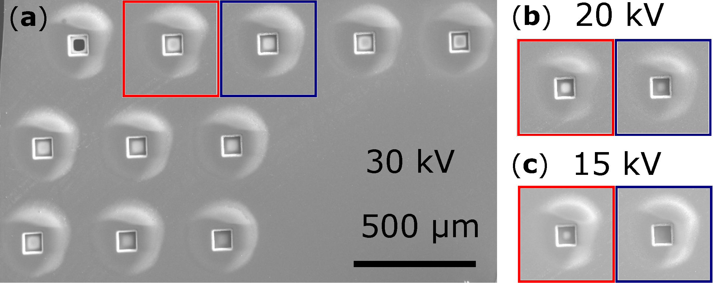
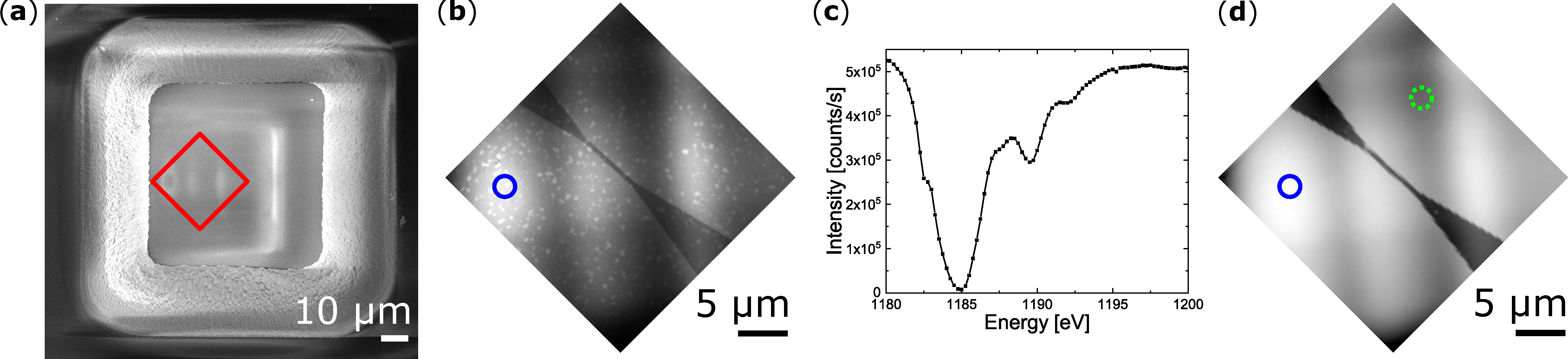
3. Results and Discussion

One of the main challenges in the fabrication of X-ray transparent windows is to accurately stop the milling process at a thickness in the range of a few hundred nanometers. Ideally, the thickness should already be determined during the fabrication process so that the milling can be adapted. To achieve an empirical in-situ transparency level determination, we correlate the transparency for soft X-rays with that for electrons from the SEM available in two-beam PFIB-SEM systems. For that purpose, the sample has to be mounted so that the electrons can be transmitted through the milled area, which means that the sample holder must not shadow the path on the opposite side of the column. In that respect, we designed a dedicated sample holder that allows for mounting samples down to about 2.5 mm × 2.5 mm (see Supplementary Material for the details of the design).
Even though direct electron transmission measurements are not possible due to geometric restrictions, we can correlate the brightness of a milled area with its transparency. This is possible because—as the milled window becomes thin enough for the primary electrons to pass through—secondary electrons can also be created at the back side of the window and reach the detector. To this end, we milled several windows with slightly different depths into a 50 µm-thick STO substrate, as shown in the SEM image at 30 kV in Figure 2a. For STO, we found a working rate of approximately 0.25 µm3/nC. Thus, in practical terms, milling one of these individual windows of 80 µm × 80 µm lateral size, using a 600 nA Xe+ ion beam, takes less than 40 min. The SEM image is taken at normal incidence to the surface to be able to fully image the inside of the milled windows. Afterwards, we measured the X-ray transmission at 1 keV through each window. By doing so, we obtained the relative X-ray transmission rates, ranging from 100% (corresponding to a hole) to about 1%. In the following, we exemplarily focus on the windows marked by the red and blue boxes in Figure 2. The window in the red box exhibits an X-ray transmission of about 50% with respect to the unattenuated beam, while the window in the blue box transmits less than 20% of the X-rays. While such a difference is hard to infer from the electron image at 30 kV (Figure 2a), the correlation with the electron transparency becomes apparent when we look at SEM images at lower electron energies. For a 20 kV acceleration voltage (Figure 2b), a difference in brightness between the two windows is visible. This becomes even more distinct at a lower energy of 15 kV (Figure 2c), where the red-framed window shows a bright spot, whereas the blue-framed window is not transparent for the electrons anymore. The bright halos around the windows stem from charging where the conductive coating on the non-conductive substrate has been removed by the halo of the PFIB beam.
While these findings on the correlation between electron and X-ray transparency cannot be directly generalized to other substrates and thin film systems, they serve as a guideline and might require adaptation to specific samples. We demonstrate such adaption by means of a second sample system: A Ga-doped Y3Fe5O12 (YIG) film of 150 nm thickness on a Gd3Ga5O12 (GGG) bulk substrate. This sample was first lapped to a thickness of approximately 120 µm. Subsequently, a window was milled into the substrate using a Xe PFIB. The initial lateral size of the window was 100 µm × 100 µm, which was reduced to about 50 µm × 50 µm during the milling process. Starting with a larger than required window size reduces redeposition effects during the final milling steps on such thick substrates. We found an approximate working rate of 0.3 µm3/nC for GGG. This given, a window similar to the previously shown STO ones (80 µm × 80 µm size into a 50 µm-thick substrate) requires approximately 30 min of milling time using a 600 nA Xe+ ion beam. The SEM image of the final window taken with the secondary electron detector at 10 kV is shown in Figure 3a.
We then use STXM to image the milled window in the second sample. At the thinnest region, an area of at least 25 µm × 25 µm is transparent for X-rays at the Fe L3 absorption edge at ~708 eV (Figure 3b). The STXM image corresponds to the area marked in red in the SEM image. When comparing the two images, one sees that areas of a bright grey level exist in the SEM image. These areas also appear as bright regions in the STXM image, which means that they are thinner than the surrounding parts. Nevertheless, spectroscopy measurements at the Gd M5 edge (Figure 3c), where the intensity drops by a factor of more than 50, demonstrate that even in these thinnest regions Gd is still present, which means that there is GGG substrate remaining everywhere. The absolute thickness of the remaining substrate can be estimated using the Beer–Lambert law I t = I 0 × e d λ [21,22,23]. For this purpose, we measured the incoming (I0) and transmitted beam (It) at a photon energy of 1150 eV. A corresponding logarithmic transmittance image is shown in Figure 3d. The 150 nm-thick Ga-doped YIG film transmits approximately 71% of the incoming beam and the GGG substrate has an absorption length λ of 0.335 µm [24]. This leads to a GGG thickness of approximately 100 nm at the thinnest point and of approximately 500 nm at a thicker point, indicated in Figure 3d by the blue and dotted green circle, respectively. These calculations additionally confirm that the PFIB only milled into the substrate while the thin film is not directly affected by the ion beam. Here, another advantage of using Xe+ ions for the milling becomes obvious: they have a lower penetration depth than conventionally used Ga ions at the same energy. For the case of GGG, the penetration depth is 11 nm for Xe+ ions compared to 14 nm for Ga+ ions, as calculated by SRIM [25]. The white spots in the STXM image are Fe-depleted film areas that do not originate from the PFIB milling. The tapered diagonal dark contrast structure in the STXM image stems from a microwave antenna, which was lithographically patterned onto the Ga:YIG film after the PFIB milling step and which is therefore not present in the corresponding SEM image. The comparison shows that even though a large area of the window is suitable for soft X-ray transmission measurements, there are small variations in thickness that already can be observed in the SEM image during fabrication, such that the milling could be adapted in situ.

4. Conclusions

We presented an approach to fabricate soft X-ray transparent windows out of bulk substrates with the use of a Xe PFIB, which benefits from the more than 10 times faster milling speeds compared to Ga FIBs. This allows us to employ plane substrates with thicknesses of the order of 100 µm prior to the PFIB milling, substantially simplifying the fabrication process. Xe PFIB facilitates the fabrication of windows as large as 100 µm x 100 µm, while plane and smooth surfaces are obtained despite the high milling speeds. To estimate the transparency level of the milled windows during fabrication, we correlate their transparency for electrons at different energies with their transmissivity for X-rays. We demonstrate the feasibility of our approach by performing STXM imaging on a sample obtained by the method described. The use of a Xe PFIB for milling soft X-ray transparent windows is widely applicable to materials that cannot be grown on amorphous SiN window substrates, especially for situations where large areas or multiple windows are needed.

Supplementary Materials

The following are available online at https://www.mdpi.com/article/10.3390/cryst11050546/s1: A pdf describing the design of the PFIB sample holder.

Author Contributions

J.R. (Jörg Raabe) and S.W. conceived the study. C.D. grew the Ga:YIG sample. A.H. supervised the STO sample processing. S.M. and S.S. performed the mechanical thinning. S.M. and J.R. (Joakim Reuteler) conducted the PFIB milling. S.M., S.F., M.W. and S.W. performed the STXM measurements. S.M. wrote the manuscript with the support of S.W. All authors discussed the results and commented on the manuscript. All authors have read and agreed to the published version of the manuscript.

Funding

This project received funding from the Swiss National Science Foundation (Grant Agreement No. 172517 and 200021_182013). C.D. acknowledges financial support by the Deutsche Forschungsgemeinschaft (DFG, German Research Foundation)—271741898. A.H. was funded by the European Union’s Horizon 2020 research and innovation programme under Marie Sklodowska-Curie grant agreement no. 794207 (ASIQS). S.W. acknowledges financial support from the Leibniz Association via grant no. K162/2018 (OptiSPIN).

Data Availability Statement

The data presented in this study are openly available at https://www.doi.org/10.5281/zenodo.4753181, accessed on 13 May 2021.

Acknowledgments

We would like to thank Elisabeth Müller, Joe Bailey, Johannes Förster and Joachim Gräfe for fruitful discussions, Michael Bechtel for support during beamtimes at Maxymus and Blagoj Sarafimov for fabrication of the PFIB sample holder. The authors acknowledge support of the Scientific Center for Optical and Electron Microscopy ScopeM of the ETH Zürich. The STXM measurements were carried out at the MAXYMUS end station of the BESSY II synchrotron radiation facility of Helmholtz-Zentrum Berlin and at the PolLux end station at SLS, PSI, Villigen PSI, Switzerland. We thank HZB for the allocation of synchrotron radiation beamtime. The PolLux end station was financed by the German Ministerium für Bildung und Forschung (BMBF) through contracts 05K16WED and 05K19WE2. This project received funding from the Swiss National Science Foundation (Grant Agreement No. 172517 and 200021_182013). C.D. acknowledges financial support by the Deutsche Forschungsgemeinschaft (DFG, German Research Foundation)—271741898. A.H. was funded by the European Union’s Horizon 2020 research and innovation programme under Marie Sklodowska-Curie grant agreement no. 794207 (ASIQS). S.W. acknowledges financial support from the Leibniz Association via grant no. K162/2018 (OptiSPIN).

Conflicts of Interest

The authors declare no conflict of interest.

References

  1. Willmott, P. Introduction to Synchrotron Radiation: Techniques and Applications; John Wiley & Sons: Chichester, UK, 2019; Volume 2. [Google Scholar]
  2. Als-Nielsen, J.; McMorrow, D. Imaging, in Elements of Modern X-ray Physics; Wiley: New York, NY, USA, 2011; pp. 305–342. [Google Scholar]
  3. Henke, B.L.; Gullikson, E.M.; Davis, J.C. X-Ray Interactions: Photoabsorption, Scattering, Transmission, and Reflection at E = 50–30,000 eV, Z = 1–92. At. Data Nucl. Data Tables 1993, 54, 181–342. [Google Scholar] [CrossRef] [Green Version]
  4. Baldrati, L.; Schneider, C.; Niizeki, T.; Ramos, R.; Cramer, J.; Ross, A.; Saitoh, E.; Kläui, M. Spin transport in multilayer systems with fully epitaxial NiO thin films. Phys. Rev. B 2018, 98, 014409. [Google Scholar] [CrossRef] [Green Version]
  5. Wadley, P.; Howells, B.; Železný, J.; Andrews, C.; Hills, V.; Campion, R.P.; Novák, V.; Olejník, K.; Maccherozzi, F.; Dhesi, S.S.; et al. Electrical switching of an antiferromagnet. Science 2016, 351, 587–590. [Google Scholar] [CrossRef] [PubMed] [Green Version]
  6. Pohl, U.W. Epitaxy of Semiconductors: Introduction to Physical Principles; Springer: Berlin/Heidelberg, Germany, 2013. [Google Scholar]
  7. Pesquera, D.; Herranz, G.; Barla, A.; Pellegrin, E.; Bondino, F.; Magnano, E.; Sánchez, F.; Fontcuberta, J. Surface symmetry-breaking and strain effects on orbital occupancy in transition metal perovskite epitaxial films. Nat. Commun. 2012, 3, 1189. [Google Scholar] [CrossRef] [PubMed]
  8. Ohtomo, A.; Hwang, H.Y. A high-mobility electron gas at the LaAlO3/SrTiO3 heterointerface. Nat. Cell Biol. 2004, 427, 423–426. [Google Scholar] [CrossRef] [PubMed]
  9. Seidel, H.; Csepregi, L.; Heuberger, A.; Baumgärtel, H. Anisotropic Etching of Crystalline Silicon in Alkaline Solutions: I. Orientation Dependence and Behavior of Passivation Layers. J. Electrochem. Soc. 1990, 137, 3612–3626. [Google Scholar] [CrossRef]
  10. Gomes, W.P. Wet Etching of III–V Semiconductors. In Handbook of Advanced Electronic and Photonic Materials and Devices; Nalwa, H.S., Ed.; Academic Press: San Diego, CA, USA, 2001; pp. 221–256. [Google Scholar]
  11. Förster, J.; Wintz, S.; Bailey, J.; Finizio, S.; Josten, E.; Dubs, C.; Bozhko, D.A.; Stoll, H.; Dieterle, G.; Träger, N.; et al. Nanoscale X-ray imaging of spin dynamics in yttrium iron garnet. J. Appl. Phys. 2019, 126, 173909. [Google Scholar] [CrossRef] [Green Version]
  12. Digernes, E.; Leliaert, J.; Weigand, M.; Folven, E.; Van Waeyenberge, B. Direct observation of temperature dependent vortex dynamics in a La0.7Sr0.3MnO3 micromagnet. Phys. Rev. Res. 2020, 2, 043429. [Google Scholar] [CrossRef]
  13. Fohler, M.; Frömmel, S.; Schneider, M.; Pfau, B.; Günther, C.M.; Hennecke, M.; Guehrs, E.; Shemilt, L.; Mishra, D.; Berger, D.; et al. A general approach to obtain soft x-ray transparency for thin films grown on bulk substrates. Rev. Sci. Instrum. 2017, 88, 103701. [Google Scholar] [CrossRef] [PubMed]
  14. Förster, J.; Gräfe, J.; Bailey, J.; Finizio, S.; Träger, N.; Groß, F.; Mayr, S.; Stoll, H.; Dubs, C.; Surzhenko, O.; et al. Direct observation of coherent magnons with suboptical wavelengths in a single-crystalline ferrimagnetic insulator. Phys. Rev. B 2019, 100, 214416. [Google Scholar] [CrossRef] [Green Version]
  15. Simmendinger, J.; Ruoss, S.; Stahl, C.; Weigand, M.; Gräfe, J.; Schütz, G.; Albrecht, J. Transmission x-ray microscopy at low temperatures: Irregular supercurrent flow at small length scales. Phys. Rev. B 2018, 97, 134515. [Google Scholar] [CrossRef] [Green Version]
  16. Baumgaertl, K.; Gräfe, J.; Che, P.; Mucchietto, A.; Förster, J.; Träger, N.; Bechtel, M.; Weigand, M.; Schütz, G.; Grundler, D. Nanoimaging of Ultrashort Magnon Emission by Ferromagnetic Grating Couplers at GHz Frequencies. Nano Lett. 2020, 20, 7281–7286. [Google Scholar] [CrossRef] [PubMed]
  17. Büttner, F.; Mawass, M.A.; Bauer, J.; Rosenberg, E.; Caretta, L.; Avci, C.O.; Gräfe, J.; Finizio, S.; Vaz, C.A.F.; Novakovic, N.; et al. Thermal nucleation and high-resolution imaging of submicrometer magnetic bubbles in thin thulium iron garnet films with perpendicular anisotropy. Phys. Rev. Mater. 2020, 4, 011401. [Google Scholar] [CrossRef] [Green Version]
  18. Träger, N.; Groß, F.; Förster, J.; Baumgaertl, K.; Stoll, H.; Weigand, M.; Schütz, G.; Grundler, D.; Gräfe, J. Single shot acquisition of spatially resolved spin wave dispersion relations using X-ray microscopy. Sci. Rep. 2020, 10, 18146. [Google Scholar] [CrossRef] [PubMed]
  19. Burnett, T.; Kelley, R.; Winiarski, B.; Contreras, L.; Daly, M.; Gholinia, A.; Burke, M.; Withers, P. Large volume serial section tomography by Xe Plasma FIB dual beam microscopy. Ultramicroscopy 2016, 161, 119–129. [Google Scholar] [CrossRef] [PubMed]
  20. Raabe, J.; Tzvetkov, G.; Flechsig, U.; Böge, M.; Jaggi, A.; Sarafimov, B.; Vernooij, M.G.C.; Huthwelker, T.; Ade, H.; Kilcoyne, D.; et al. PolLux: A new facility for soft x-ray spectromicroscopy at the Swiss Light Source. Rev. Sci. Instrum. 2008, 79, 113704. [Google Scholar] [CrossRef] [PubMed]
  21. Bouguer, P. Essai d’Optique sur la Gradation de la Lumière. J. Röntgen Soc. 1922, 18, 93. [Google Scholar] [CrossRef]
  22. Lambert, J.H. Photometria, Sive de Mensura et Gradibus Luminis, Colorum et Umbrae; Sumptibus Vidae Eberhardi Klett: Augsburg, Germany, 1760. [Google Scholar]
  23. Beer, A. Bestimmung der Absorption des rothen Lichts in farbigen Flüssigkeiten. Ann. Phys. Chem. 1852, 86, 78–88. [Google Scholar] [CrossRef] [Green Version]
  24. X-Ray Interactions with Matter [Internet]. Available online: https://henke.lbl.gov/optical_constants/ (accessed on 23 April 2021).
  25. Ziegler, J.F.; Ziegler, M.; Biersack, J. SRIM—The stopping and range of ions in matter (2010). Nucl. Instrum. Methods Phys. Res. Sect. B Beam Interact. Mater. At. 2010, 268, 1818–1823. [Google Scholar] [CrossRef] [Green Version]
Figure 1. Thinning process. (a) Thin film (red) grown on a substrate (grey) is glued onto a glass support (blue). (b) In the mechanical lapping/polishing step, part of the substrate is removed to a total thickness between 50 µm and 120 µm. (c) For the PFIB processing, the sample is removed from the glass and a conductive layer (orange) is optionally deposited. (d) More material is selectively removed with the Xe PFIB in the desired areas of the sample until a final thickness of the order of several hundreds of nanometers is reached in these windows. (e) SEM image of a window milled into STO taken at a tilt of 55° with respect to the surface normal.
Crystals 11 00546 g001
Figure 2. SEM images, acquired with the secondary electron detector, of windows with varying thicknesses in a 50 µm-thick STO substrate at different electron acceleration voltages. (a) Overview of windows at 30 kV. The windows in the red and blue boxes are additionally shown for 20 kV (b) and 15 kV (c).
Crystals 11 00546 g002
Figure 3. Comparison of transmissivity between electrons and soft X-rays of a Ga-doped YIG film grown on GGG. (a) Scanning electron micrograph at 10 kV. (b) STXM image of the detail indicated by the red square in (a) taken at the Fe L3 edge. (c) X-ray transmission spectrum at the Gd M5 edge taken at the thinnest position indicated by the blue circle in (b). (d) Logarithmic transmittance of the window taken at 1150 eV. The blue and dotted green circles indicate the points for the thickness calculation.
Crystals 11 00546 g003
Publisher’s Note: MDPI stays neutral with regard to jurisdictional claims in published maps and institutional affiliations.

