
Morphological and Structural Characterization of Magnetron-Sputtered Aluminum and Aluminum-Boron Thin Films


Abstract
1. Introduction
2. Experimental and Characterization
2.1. Materials
2.2. Thin Films
2.3. Characterization
2.3.1. Surface Morphology
2.3.2. Crystal Structure
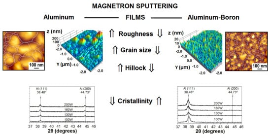
3. Results and Discussion
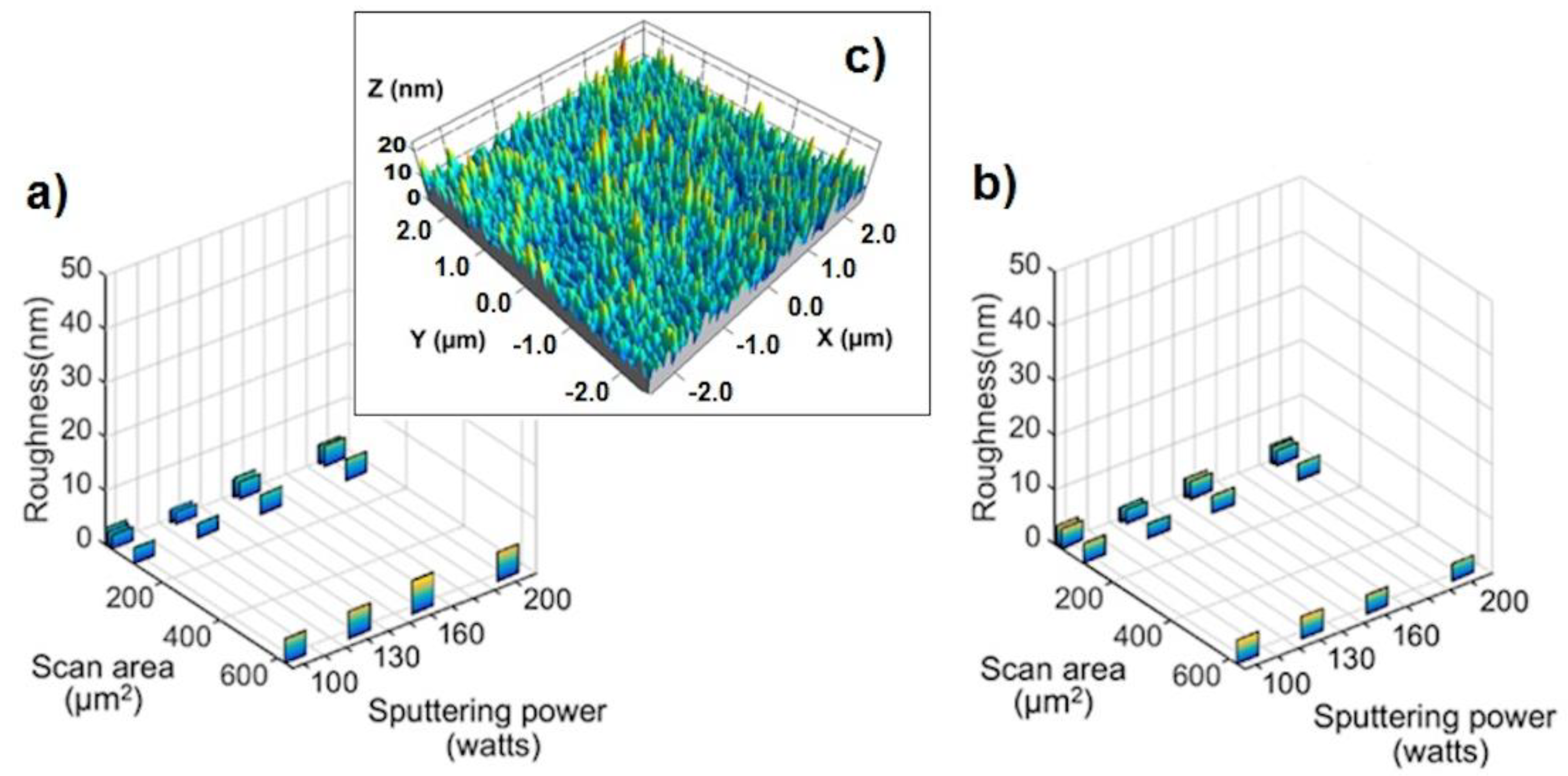
3.1. Surface Morphology
3.1.1. RMS Assessment
3.1.2. Substrate Effects
3.1.3. Average Grain Size
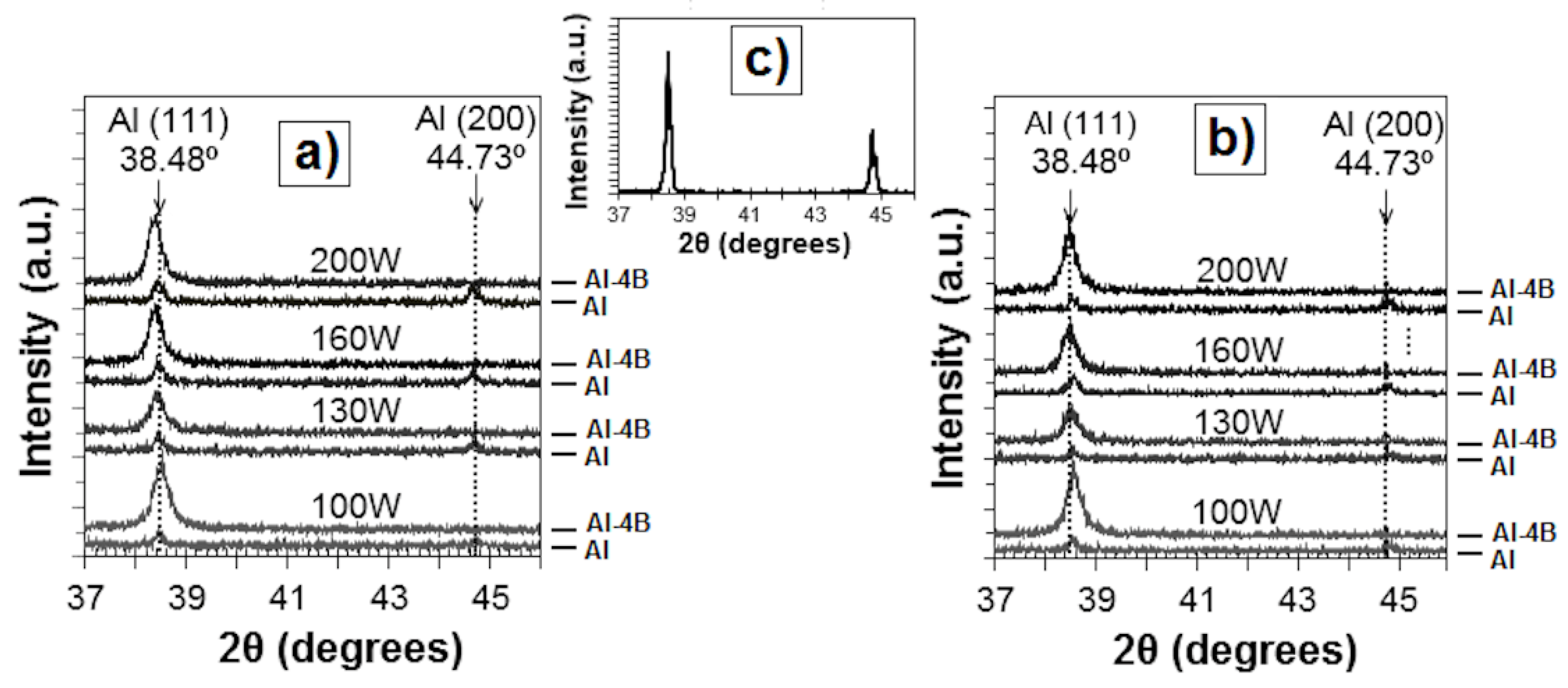
3.2. Structural Evaluation
4. Conclusions
Author Contributions
Funding
Institutional Review Board Statement
Informed Consent Statement
Data Availability Statement
Acknowledgments
Conflicts of Interest
Appendix A

References
- Khachatryana, H.; Leeb, S.-N.; Kimc, K.-B.; Kimd, H.-K.; Kim, M. Al thin film: The effect of substrate type on Al film formation and morphology. J. Phys. Chem. Solids 2018, 122, 109–117. [Google Scholar] [CrossRef]
- Ottone, C.; Laurenti, M.; Bejtka, K.; Sanginario, A.; Cauda, V. The Effects of the Film Thickness and Roughness in the Anodization Process of Very Thin Aluminum Films. J. Mater. Sci. Nanotechnol. 2014, 1, 1–9. [Google Scholar] [CrossRef]
- Hwang, S.; Lee, J.; Jeong, C.; Joo, Y. Effect of film thickness and annealing temperature on hillock distributions in pure Al films. Scr. Mater. 2007, 56, 17–20. [Google Scholar] [CrossRef]
- Quintana, P.; Oliva, A.I.; Ceh, O.; Corona, J.E. Thickness effects on aluminum thin films. Superf. Vacío. 1999, 9, 280–282. Available online: https://www.fis.cinvestav.mx/~smcsyv/supyvac/9/sv928099.pdf (accessed on 31 March 2021).
- Kang, T.J.; Kim, J.-G.; Lee, H.-Y.; Lee, J.-S.; Lee, J.-H.; Hahn, J.-H.; Kim, Y.H. Modification of Optical and Mechanical Surface Properties of Sputter-Deposited Aluminum Thin Films through Ion Implantation. Int. J. Precis. Eng. Man. 2014, 15, 889–894. [Google Scholar] [CrossRef]
- Kylner, C.; Mattsson, L. Enhanced optical performance of aluminum films by copper inclusion. Thin Solid Film 1999, 348, 222–226. [Google Scholar] [CrossRef]
- Barron, L.W.; Neidrich, J.; Kurinec, S.K. Optical, electrical, and structural properties of sputtered aluminum alloy thin films with copper, titanium and chromium additions. Thin Solid Films 2007, 515, 3363–3372. [Google Scholar] [CrossRef]
- Basaran, C.; Lin, M. Damage mechanics of electromigration induced failure. Mech. Mater. 2008, 40, 66–79. [Google Scholar] [CrossRef]
- Onoda, H.; Narita, T.; Touchi, K.; Hashimoto, K. Effects of insulator surface roughness on Al-alloy film properties and electromigration performance in Al-alloy/Ti insulator layered interconnects. J. Vac. Sci. Technol. B 1996, 14, 2645–2655. [Google Scholar] [CrossRef]
- Black, J.R. Electromigration failure modes in aluminum metallization for semiconductor devices. Proc. IEEE 1969, 57, 1587–1594. [Google Scholar] [CrossRef]
- Ramos, G.; Suárez, O.M. Characterization of sputtered Al-B-Si thin films produced with composite targets for device applications. Sci. Eng. Compos. Mater. 2012, 19, 93–99. [Google Scholar] [CrossRef]
- Onishi, T.; Iwamura, E.; Takagi, K. Effects of Nd content in Al thin films on hillock formation. J. Vac. Sci. Technol. A 1997, 15, 2339–2348. [Google Scholar] [CrossRef]
- Wu, Z.; Bai, Y.; Qu, W.; Wu, A.; Zhang, D.; Zhao, J.; Jiang, X. Al-Mg-B thin films prepared by magnetron sputtering. Vacuum 2010, 85, 541–545. [Google Scholar] [CrossRef]
- Draissia, M.; Boudemagh, H.; Debili, M.Y. Structure and Hardness of the Sputtered Al-Cu Thin Films System. Phys. Scr. 2004, 69, 348–350. [Google Scholar] [CrossRef]
- Ishiguro, T.; Miyamura, K. Controllability of Mesoscopic Surface Roughness of Sputtered Al and Al-N Films. Mater. Trans. 2005, 46, 3037–3043. [Google Scholar] [CrossRef][Green Version]
- Melgarejo, Z.H.; Suárez, O.M.; Sridharan, K. Microstructure and properties of functionally graded Al-Mg-B composites fabricated by centrifugal casting. Compos. Part A Appl. Sci. Manuf. 2008, 39, 1150–1158. [Google Scholar] [CrossRef]
- Adelakin, T.K.; Suárez, O.M. Study of Boride-Reinforced Aluminum Matrix Composites Produced via Centrifugal Casting. Mater. Manuf. Process 2011, 26, 338–345. [Google Scholar] [CrossRef]
- Barajas-Valdes, U. Study of Light Weight, High Strength, Multifunctional Composite Material: Aluminum Reinforced with AlB2 Particles. Ph.D. Dissertation, Departmente of Civil Engineering, University of Puerto Rico, Mayaguez, Puerto Rico, 2017. Available online: https://scholar.uprm.edu/handle/20.500.11801/910 (accessed on 31 March 2021).
- Barajas-Valdes, U.; Suárez, O.M. Nanomechanical properties of thin films manufactured via magnetron sputtering from pure aluminum and aluminum-boron targets. Thin Solid Films 2020, 693, 137670–137679. [Google Scholar] [CrossRef]
- Bordo, K.; Rubahn, H. Effect of Deposition Rate on Structure and Surface Morphology of Thin Evaporated Al Films on Dielectrics and Semiconductors. Mater. Sci. Medzg. 2012, 18, 313–317. [Google Scholar] [CrossRef]
- Jang, K.-H.; Hwang, S.-J.; Joo, Y.-C. Effect of capping layer on hillock formation in thin Al films. Met. Mater. Int. 2008, 14, 147–150. [Google Scholar] [CrossRef]
- Barron, L.W. High-Reflectance, Sputter-Deposited Aluminum Alloy Thin Films for Micro-Electro-Mechanical Systems. Master’s Thesis, Department of Materials Science and Engineering, Rochester Institute of Technology, Rochester, NY, USA, 2005. Available online: https://scholarworks.rit.edu/theses/5760/ (accessed on 31 March 2021).
- Kim, D.; Heiland, B.; Nix, W.D.; Arzt, E.; Deal, M.D.; Plummer, J.D. Microstructure of thermal hillocks on blanket Al thin films. Thin Solid Films 2000, 371, 278–282. [Google Scholar] [CrossRef]
- Martin, B.C.; Tracy, C.J.; Mayer, J.W.; Hendrickson, L.E. A comparative study of hillock formation in aluminum films. Thin Solid Films 1995, 271, 64–68. [Google Scholar] [CrossRef]
- Raić, K.T. An explanation of hillock growth in thin Al films. Surf. Eng. 2016, 32, 1–6. [Google Scholar] [CrossRef]
- Smith, D. Thin-Film Deposition. Principles and Practice; McGraw-Hill: New York, NY, USA, 1995; pp. 178–301. [Google Scholar]
- Ohring, M. The Materials Science of Thin Films, 2nd ed.; Academic Press: San Diego, CA, USA, 2002; pp. 403–449. [Google Scholar]
- Aceto, S.; Chang, C.Y.; Vook, R.W. Hillock growth on aluminum and aluminum alloy films. Thin Solid Films 1992, 219, 80–86. [Google Scholar] [CrossRef]
- Aurongzeb, D.; Washington, E.; Basavaraj, M.; Berg, J.M.; Temkin, H.; Holtz, M. Nanoscale surface roughening in ultrathin aluminum films. Appl. Phys. 2006, 100, 11–14. [Google Scholar] [CrossRef]
- Montgomery, D.C.; Runger, G.C. Applied Statistics and Probability for Engineers, 3rd ed.; John Wiley & Sons: New York, NY, USA, 2003; pp. 207–219. [Google Scholar]
- Paul, A.; Wingbermu, J. Surface morphology for ion-beam sputtered Al layer with varying sputtering conditions. Appl. Surf. Sci. 2006, 252, 8151–8155. [Google Scholar] [CrossRef]
- Le, M.-T.; Sohn, Y.-U.; Lim, J.-W.; Choi, G.-S. Effect of Sputtering Power on the Nucleation and Growth of Cu Films Deposited by Magnetron Sputtering. Mater. Trans. 2010, 51, 116–120. [Google Scholar] [CrossRef]
- Ramos-Rivera, G. Fabrication, Characterization and Testing of Functionally Graded Aluminum-based Targets for Sputtering Deposition of Hybrid Composites. Master’s Thesis, Department of Mechanical Engineering, University of Puerto Rico, Mayagüez, Puerto Rico, 2011. Available online: https://scholar.uprm.edu/handle/20.500.11801/429 (accessed on 31 March 2021).
- Venables, J.; Spiller, G.; Hanbucken, M. Nucleation and growth of thin films. Rep. Prog. Physic. 1984, 47, 399–459. Available online: https://iopscience.iop.org/article/10.1088/0034-4885/47/4/002 (accessed on 31 March 2021). [CrossRef]
- Reichelt, K. Nucleation and Growth of Thin Films. Vacuum 1988, 38, 1083–1099. [Google Scholar] [CrossRef]
- Franssila, S. Thin-film Growth and Structure. In Introduction to Microfabrication, 1st ed.; Franssila, S., Ed.; John Wiley & Sons: England, UK, 2004; pp. 73–90. [Google Scholar]
- Jeong, S.H.; Kho, S.; Jung, D.; Lee, S.B.; Boo, J. Deposition of aluminum-doped zinc oxide films by RF magnetron sputtering and study of their surface characteristics. Surf. Coat. Technol. 2003, 175, 187–192. [Google Scholar] [CrossRef]
- Thompson, C.V.; Carel, R. Texture development in polycrystalline thin films. Mater. Sci. Eng. B 1995, 32, 211–219. [Google Scholar] [CrossRef]
- Simon, A.H. Sputter Processing. In Handbook of Thin Film Deposition. Tech. Process. Technol, 3rd ed.; Seshan, K., Ed.; Elsevier Inc.: Oxford, UK, 2012; pp. 55–73. [Google Scholar]
- Chaoumead, A.; Sung, Y.W.; Kwak, D. The Effects of RF Sputtering Power and Gas Pressure on Structural and Electrical Properties of ITiO Thin Film. Adv. Condens. Matte Phys. 2012, 2012, 1–7. [Google Scholar] [CrossRef]
- Cullity, B.D.; Stock, S.R. Elements of X-ray Diffraction, 3rd ed.; Pearson New International: England, UK, 2014; pp. 237–239. [Google Scholar]
- Chen, Y.; Bakshi, S.R.; Agarwal, A. Correlation between nanoindentation and nanoscratch properties of carbon nanotube reinforced aluminum composite coatings. Surf. Coat. Technol. 2010, 204, 2709–2715. [Google Scholar] [CrossRef]


| Substrate | Silicon Wafer | Glass Slide | ||||||||
|---|---|---|---|---|---|---|---|---|---|---|
| Material | Al-4B films | |||||||||
| Sputtering Power | Scan Area (µm2) | Scan Area (µm2) | ||||||||
| (watts) | 2.25 | 9 | 25 | 100 | 625 | 2.25 | 9 | 25 | 100 | 625 |
| 100 | 3.11 | 3.21 | 3.63 | 3.48 | 4.31 | 3.11 | 2.63 | 2.57 | 2.75 | 4.45 |
| 130 | 2.14 | 2.17 | 2.51 | 2.48 | 4.12 | 1.75 | 2.11 | 2.26 | 2.74 | 5.03 |
| 160 | 2.82 | 2.96 | 3.16 | 3.09 | 3.36 | 2.92 | 3.09 | 3.29 | 3.51 | 6.01 |
| 200 | 2.91 | 2.74 | 2.66 | 2.93 | 3.14 | 3.20 | 3.62 | 3.95 | 3.96 | 5.28 |
| Error Bar | 0.09 | 0.17 | ||||||||
| RMS Average | 3.05 | 3.41 | ||||||||
| Material | Aluminum Films | |||||||||
| Sputtering Power | Scan Area (µm2) | Scan Area (µm2) | ||||||||
| (watts) | 2.25 | 9 | 25 | 100 | 625 | 2.25 | 9 | 25 | 100 | 625 |
| 100 | 20.35 | 21.20 | 46.13 | 19.27 | 27.86 | 14.52 | 17.34 | 23.12 | 33.53 | 29.36 |
| 130 | 15.94 | 14.75 | 25.66 | 33.71 | 33.39 | 17.43 | 15.94 | 17.99 | 31.90 | 35.91 |
| 160 | 9.39 | 13.93 | 32.35 | 29.60 | 28.48 | 11.90 | 12.85 | 16.24 | 26.32 | 31.99 |
| 200 | 17.68 | 27.29 | 31.57 | 30.47 | 25.49 | 18.50 | 23.93 | 29.09 | 31.45 | 29.93 |
| Error Bar | 1.34 | 1.19 | ||||||||
| RMS Average | 25.23 | 23.46 | ||||||||
| Film | Al-4B | Aluminum | ||||||
|---|---|---|---|---|---|---|---|---|
| Substrate | Silicon Wafer | Glass Slide | Silicon Wafer | Glass Slide | ||||
| Scan Area (µm2) | Thickness (nm) | Thickness (nm) | Thickness (nm) | Thickness (nm) | ||||
| 100 | 500 | 100 | 500 | 100 | 500 | 100 | 500 | |
| RMS roughness | RMS Roughness | |||||||
| 0.25 | 1.67 | 2.27 | 1.89 | 2.47 | 6.13 | 12.51 | 9.20 | 13.26 |
| 1.00 | 1.80 | 2.19 | 2.15 | 2.53 | 8.12 | 23.60 | 8.98 | 18.94 |
| 2.25 | 1.92 | 2.27 | 2.31 | 3.07 | 8.33 | 14.85 | 8.96 | 12.83 |
| 9.00 | 2.21 | 2.48 | 2.67 | 3.34 | 8.13 | 18.81 | 8.98 | 17.47 |
| 25.00 | 2.64 | 2.93 | 3.30 | 3.68 | 12.55 | 28.02 | 9.00 | 16.56 |
| Average RMS | 2.05 | 2.43 | 2.47 | 3.02 | 8.65 | 19.56 | 9.02 | 15.81 |
| Material | Al | Al-4B | ||||
|---|---|---|---|---|---|---|
| Sputtering Power | Diameter | STD | Cv | Diameter | STD | Cv |
| (Watts) | (nm) | (nm) | ||||
| 100 | 117.24 | 57.40 | 0.49 | 97.12 | 31.37 | 0.32 |
| 130 | 118.98 | 46.87 | 0.39 | 90.21 | 24.80 | 0.27 |
| 160 | 150.34 | 66.26 | 0.44 | 75.66 | 29.05 | 0.38 |
| 200 | 152.14 | 86.59 | 0.57 | 79.20 | 20.69 | 0.26 |
| Target Material | Al-4B | Al | ||||
|---|---|---|---|---|---|---|
| Substrate | Silicon Wafer | |||||
| Sputtering Power | 2θ | d | a | 2θ | d | a |
| (watts) | (degrees) | (nm) | (nm) | (degrees) | (nm) | (nm) |
| 100 | 38.581 | 0.2334 | 0.4042 | 38.562 | 0.2335 | 0.4044 |
| 130 | 38.531 | 0.2343 | 0.4047 | 38.557 | 0.2341 | 0.4044 |
| 160 | 38.492 | 0.2344 | 0.4051 | 38.549 | 0.2340 | 0.4045 |
| 200 | 38.489 | 0.2345 | 0.4051 | 38.559 | 0.2341 | 0.4044 |
| Substrate | Glass Slide | |||||
| Sputtering Power | 2θ | d | a | 2θ | d | a |
| (watts) | (degrees) | (nm) | (nm) | (degrees) | (nm) | (nm) |
| 100 | 38.507 | 0.2338 | 0.4049 | 38.461 | 0.2341 | 0.4054 |
| 130 | 38.422 | 0.2343 | 0.4058 | 38.455 | 0.2341 | 0.4055 |
| 160 | 38.405 | 0.2344 | 0.4060 | 38.446 | 0.2341 | 0.4055 |
| 200 | 38.378 | 0.2345 | 0.4062 | 38.445 | 0.2341 | 0.4056 |
Publisher’s Note: MDPI stays neutral with regard to jurisdictional claims in published maps and institutional affiliations. |
© 2021 by the authors. Licensee MDPI, Basel, Switzerland. This article is an open access article distributed under the terms and conditions of the Creative Commons Attribution (CC BY) license (https://creativecommons.org/licenses/by/4.0/).
Share and Cite
Barajas-Valdes, U.; Suárez, O.M. Morphological and Structural Characterization of Magnetron-Sputtered Aluminum and Aluminum-Boron Thin Films. Crystals 2021, 11, 492. https://doi.org/10.3390/cryst11050492
Barajas-Valdes U, Suárez OM. Morphological and Structural Characterization of Magnetron-Sputtered Aluminum and Aluminum-Boron Thin Films. Crystals. 2021; 11(5):492. https://doi.org/10.3390/cryst11050492
Chicago/Turabian StyleBarajas-Valdes, Ulises, and Oscar Marcelo Suárez. 2021. "Morphological and Structural Characterization of Magnetron-Sputtered Aluminum and Aluminum-Boron Thin Films" Crystals 11, no. 5: 492. https://doi.org/10.3390/cryst11050492
APA StyleBarajas-Valdes, U., & Suárez, O. M. (2021). Morphological and Structural Characterization of Magnetron-Sputtered Aluminum and Aluminum-Boron Thin Films. Crystals, 11(5), 492. https://doi.org/10.3390/cryst11050492