Review

Epitaxy of LiNbO3: Historical Challenges and Recent Success

by
Bill Zivasatienraj
1,
M. Brooks Tellekamp
2 and
W. Alan Doolittle
1,*
1
Georgia Institute of Technology, School of Electrical and Computer Engineering, Atlanta, GA 30332, USA
2
National Renewable Energy Laboratory, Materials, Chemical, and Computational Science Directorate, Golden, CO 80401, USA
*
Author to whom correspondence should be addressed.
Crystals 2021, 11(4), 397; https://doi.org/10.3390/cryst11040397
Submission received: 16 March 2021 / Revised: 2 April 2021 / Accepted: 6 April 2021 / Published: 9 April 2021
(This article belongs to the Special Issue New Trends in Lithium Niobate: From Bulk to Nanocrystals)

Abstract

:
High-quality epitaxial growth of thin film lithium niobate (LiNbO3) is highly desirable for optical and acoustic device applications. Despite decades of research, current state-of-the-art epitaxial techniques are limited by either the material quality or growth rates needed for practical devices. In this paper, we provide a short summary of the primary challenges of lithium niobate epitaxy followed by a brief historical review of lithium niobate epitaxy for prevalent epitaxial techniques. Available figures of merit for crystalline quality and optical transmission losses are given for each growth method. The highest crystalline quality lithium niobate thin film was recently grown by halide-based molecular beam epitaxy and is comparable to bulk lithium niobate crystals. However, these high-quality crystals are grown at slow rates that limit many practical applications. Given the many challenges that lithium niobate epitaxy imposes and the wide variety of methods that have unsuccessfully attempted to surmount these barriers, new approaches to lithium niobate epitaxy are required to meet the need for simultaneously high crystalline quality and sufficient thickness for devices not currently practical by existing techniques.

Graphical Abstract

1. Introduction

Lithium niobate (LiNbO3: LN) is a mature material that has been pivotal in the advancement of optical and acoustic technology. With excellent ferro-electric, electro-optic, and piezoelectric properties, LN is incorporated into devices such as waveguides, modulators, frequency-doubled lasers, surface acoustic wave (SAW) devices, optical switches, and acoustic resonators [1]. These applications typically require high-quality, single-crystal LN to avoid optical and acoustic propagation losses. Presently, bulk LN material is being grown via the Czochralski pulling method to ensure the highest quality material. However, realization of LN in the miniaturization of devices, integration into hybrid systems, and the lowering of operational voltages for various electro-optical or electro-acoustic devices require thin layers of high-quality material. Thus, the deposition of high-quality, single-crystal thin films of LN has been a topic of research for at least three decades.
Traditionally, optical waveguides are formed in bulk substrates by techniques such as titanium (Ti) in-diffusion [2,3,4]. Compared to theoretical epitaxial counterparts, Ti-in-diffused LN has increased optical losses and the inability to form sharp index profiles as well as a top only contact structure, which leads to large voltage requirements for index modulation [5,6]. In the absence of acceptable epitaxial deposition methods, the use of ion implantation to uniformly damage and slice thin layers of LN, known as smart-cut [7] or ion-sliced LN, is presently favored. Smart-cut LN can be bonded to metal electrodes or various dielectrics, enabling lower voltage and lower loss operation, but requires a significant minimum thickness (>300 nm) [8] for wafer bonding and the transfer of the thin film, is limited to less than a few microns due to the limitations in implant energies [9], and has associated straggle-related damage, which then requires treatment for the resulting rough surface and high-temperature thermal annealing to restore optoelectrical properties [7,9]. Smart-cut LN provides a final LN wafer quality similar to bulk LN, but the thickness range available is not ideally suitable for the coupling of light on and off the chip, for example, to/from large core fibers or nanoscale integrated optics. Promising work on direct etching of LN to fabricate compact optical devices with optical propagation losses as low as 0.027 dB/cm has been shown in a 250 nm thin LN slab, achieved by a dry etch process to pattern a 600 nm smart-cut film [10,11]. Thus, high-quality epitaxial thin film LN is desirable for smaller devices with lower power consumption; lower optical losses; tighter wave confinement; integrated devices; and engineered material advances, such as doping [12,13] or strain manipulation [14], analogous to compound semiconductor electronics technology.
In this work, we will discuss the epitaxy of LN, the challenges that researchers have faced, and review the major accomplishments in LN epitaxy to date. Since some researchers target optical usage, while others merely report structural figures of merit, film quality will be detailed via metrics of optical coupling loss; deviation from single crystallinity, such as texturing of near-crystalline material; and even polycrystalline or amorphous material and the existence of rotational domains, whenever these are reported. These factors prevent or limit the practical application of LN thin epitaxial films and are the consequence of imperfections during epitaxy. Of particular interest are the elimination of rotational domains, as this has been shown to strongly effect optical quality [15,16]. There are various epitaxial methods that have successfully grown LN, including liquid phase epitaxy (LPE) [17,18,19,20,21,22,23,24,25,26], sputtering [12,14,27,28,29,30,31,32,33,34,35,36,37,38,39,40], chemical vapor deposition (CVD) [41,42,43,44,45,46,47,48,49,50], pulsed laser deposition (PLD) [13,51,52,53,54,55,56,57,58,59,60,61,62,63,64,65], and molecular beam epitaxy (MBE) [66,67,68,69,70,71,72,73,74,75,76,77]. Herein, we will view each of the epitaxial methods mentioned above from a historical perspective with a brief projection of prospects. When growing crystals with hexagonal symmetry, it is commonly found that the basal plane—the highest atomic density plane—grows the slowest, and thus is the most stable for epitaxy. Therefore, the epitaxy of LiNbO3 is generally preferred along either the 0001 or the 000 1 ¯ orientation to avoid rapidly growing facets that lead to rough surfaces and domain formation. We note that MBE has achieved the highest crystalline perfection with respect to crystalline tilt, with X-ray diffraction rocking curve figures of merit as low as 8.6 arcseconds [77] for a basal plane, 0006 reflection, comparable to congruently grown bulk LN, as shown in Figure 1. However, to date, no method has simultaneously achieved the required quality needed for optical or acoustic devices along with practical deposition rates necessary for thick devices on the scale of optical (hundreds of nm) or acoustic wavelengths (microns).

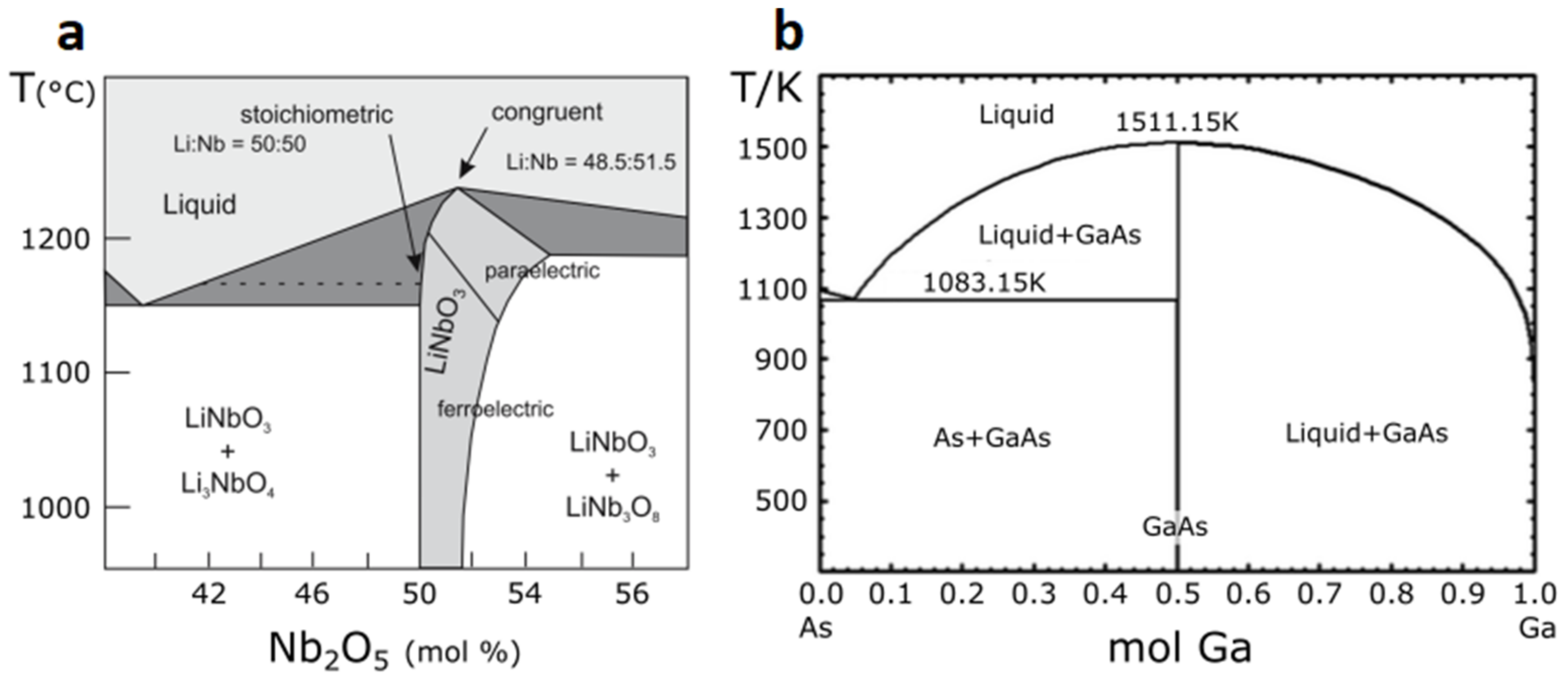
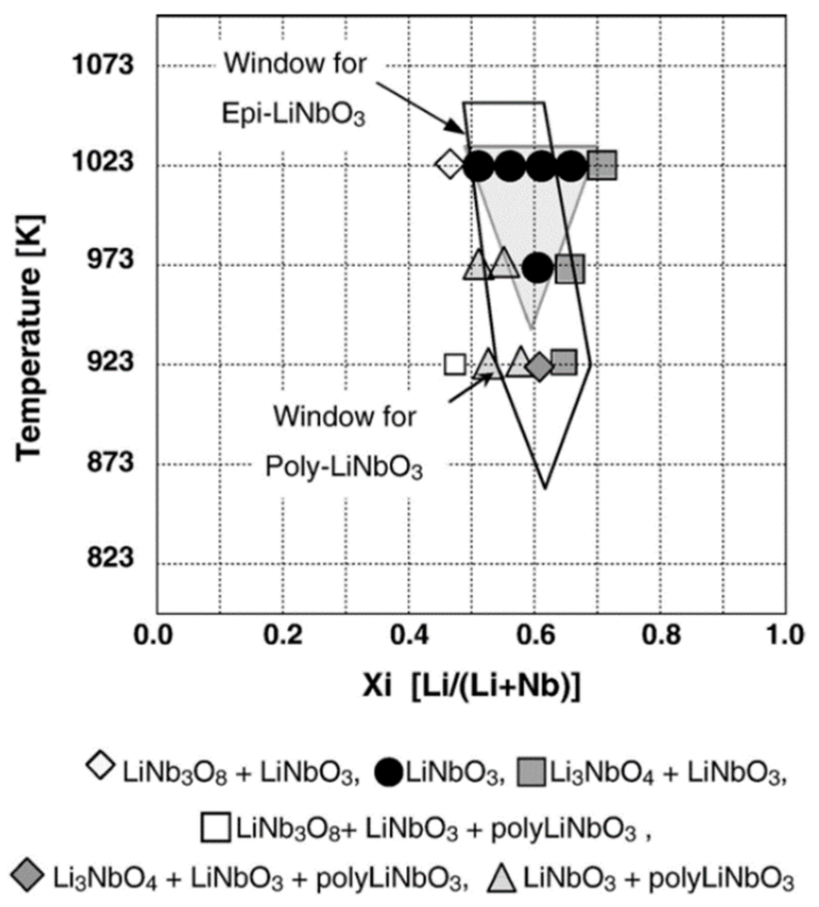
2. The Technical Challenge

Lithium niobate is a remarkable crystal and, in many ways, is anomalous in the chemical world. Lithium (Li) is among the most reactive elements known, has an enormous vapor pressure compared with most elements, and readily forms stable oxides. On the other hand, niobium (Nb) is very slow to form oxides [76] and has a negligible vapor pressure except at extreme temperatures. Furthermore, Nb forms compounds of various oxidation states leading to a strong tendency to form undesirable phases, often with overlapping phase space windows resulting in undesirable multi-phase films [78]. This complexity is further exemplified by the comparison of the phase diagrams of bulk LN [78] and gallium arsenide [79] (GaAs), as shown in Figure 2. LiNbO3 is not like most other crystals, as its congruent melting point favors a Li2O-deficient stoichiometry that is difficult to reproduce outside of bulk crystal growth. Creating particular difficulty is the fact that unlike all commercially successful materials that use epitaxy, exemplified by GaAs in Figure 2b, LiNbO3 does not have a line composition. Line compositions assure that regardless of the anion to cation ratio over a wide applicability range, nature takes care of forming the desired crystalline phase—GaAs in this example. In MBE, for instance, GaAs is formed whether the As to Ga flux ratio is 3:1 or 40:1. The difficulty of this lack of line composition for LN epitaxy cannot be understated. Thus, any change in the flux ratio of the cations to each other or cations to anions can result in a different stoichiometry or even multiple phases. Different ratios of Li to Nb form slightly differing material and this stoichiometry effects optical and acoustic properties as well as phase and crystal structure (LiNbO3, LiNbO2 [80,81], LiNb3O8 [39,49,80], Li3NbO4 [39,49,80]) by single digit percentage changes in fluxes. The lack of a line composition affects every aspect of LN epitaxial research, results in extreme tolerance limits on required flux ratios, and if commercial epitaxy is to ever be achieved, will dominate the challenges of scalability, uniformity, and yield.
In physical vapor deposition (PVD) methods, the disparity in vapor pressures between Li and Nb has not only resulted in difficult flux delivery challenges and the need for novel approaches, but the inability to keep Li on the surface without desorption typically results in the need for huge Li overpressures and surface coverages that are exponentially related to temperature, and thus, hard to control. Much of the success in recent years of the PVD methods (MBE, sputtering, and PLD) revolves around hybrid methods of generating Nb fluxes by, for example, using higher vapor pressure forms of Nb and/or using non-stoichiometric target chemistries. Contrarily, the primary challenge for CVD epitaxial methods is not generating high-vapor pressure Nb fluxes but controlling the diverse reactivity of the Nb and Li precursors that often react detrimentally with other byproducts, such as water or hydrocarbons. Each method of epitaxy deserves a full review to illuminate the subtleties in the techniques. Instead, this paper summarizes the key ideas and advances in each approach, allows the reader to compare figures of merit, and draws a conclusion on the present status of this now 48-year-old quest for high-quality LiNbO3 epitaxy, a quest that unfortunately remains unfulfilled. The order of discussion of historical results follows from the earliest work to the most successful recent work.

3. Liquid Phase Epitaxy (LPE)

In 1973, Miyazawa [82] tried to melt bulk LN crystals onto a LiTaO3 substrate to obtain a thin film of LN using a method he called epitaxial growth by melting (EGM). Although Miyazawa [82] was able to show some light propagation within the film, the crystal quality was poor, and optical losses were >5 dB/cm [19]. Miyazawa then decided to use LPE instead in Kondo et al. [20], looking at Li2O-V2O5 as a flux material, and was able to grow high-crystallinity single-crystal LN on LiTaO3 substrates, although the surface was rough and with many microcracks. Despite the film imperfections, the LPE growth in Kondo et al. [20] performed much better than EGM, with optical losses of 5 dB/cm, but at visible wavelengths, a 20–30 dB/cm optical loss was measured [19]. Ballman et al. [18] then looked at four additional flux systems, two with Li+ rich environments and two with a Nb+ rich environment. Ballman et al. [18] found that by using a Nb+ rich flux system and growing at a higher temperature, they could adjust the Li/Nb ratio in the melt to obtain lattice parameters that better matched the substrate. They also looked at different crystallographic orientations of the substrate and combined those results with an annealing process in order to grow smoother films. Ballman et al. [18] were largely successful at demonstrating optical waveguiding in LPE LN films, reporting optical losses of 1–5 dB/cm at 632.8 nm. The optical losses observed decreased with a higher crystallinity film due to scattering reduction [18,19]. Baudrant et al. [21] then used the flux system in Kondo et al. [19,82], Li2O-V2O5, and looked at different crystallographic orientations of the substrate to improve growth quality, thereby obtaining results that suggest a layer-by-layer growth mechanism of LN [21]. In 1991, Tamada et al. [22] used the same Li2O-V2O5 flux system to grow on lattice-matched (0.08% mismatch) MgO-doped LN substrates, achieving high-quality thin films with an XRD rocking curve of 11 arcseconds, but still saw large optical losses of 25 dB/cm at 514.5 nm. However, Tamada et al. [22] were able to characterize and reduce the optical losses caused by vanadium incorporation from the flux using a 600 °C ozone anneal. Later, Tamada et al. [22] produced a high-quality LN film with a low optical loss of 1.6 dB/cm, even though they were not able to remove all of the vanadium impurities. Consequently, Yamada et al. [23] later utilized a Li2O-B2O3 flux system to grow comparatively high-quality films with XRD rocking curves of 11.4 arcseconds, as shown in Figure 3, but this time without any detectable impurity inclusions and, therefore, lower optical losses of <1 dB/cm at 458 nm. Efforts toward the LPE epitaxy of LN continue and have looked at alternative growth parameters, such as using K2O fluxes [24], doping [25], and even using LPE to grow LN waveguides in laser cut channels [26] and continue as one of the lowest optical loss sources for single crystal epitaxial LN [23].

4. Sputtering

Following an unpublished work by Fukunishi et al. [27], Takada et al. [28] crushed LN single crystals into a powder to sinter into a sputtering target. Using an argon and oxygen gas mixture, Takada et al. [28] were able to sputter LN onto a heated sapphire substrate, and then demonstrate light propagation in the epitaxially grown c-axis-oriented film with optical losses of around 9 dB/cm. Jain and Hewig [29] later repeated the sputtering process by Fukunishi et al. [27], but onto a Gd3Ga5O12 substrate to phase-match with the LN for second-harmonic generation [29]. However, the films were still rough and polycrystalline, thereby contributing to higher (unreported) propagation losses. Hewig et al. [30] studied the sputtering of LN onto both amorphous and single-crystal substrates while using different deposition parameters to investigate how the various conditions affect the LN film. Hewig et al. [30] concluded that using higher temperatures and single-crystal substrates helped avoid amorphous LN films, but the resulting film was polycrystalline of 01 1 ¯ 2 -preferred orientation. The amorphous LN films showed lower optical losses of 3 dB/cm, while the polycrystalline films measured very high losses of about 10 dB/cm due to scattering at the grain boundaries. To obtain low-loss, monocrystalline material for waveguides, Hewig et al. [30] states that the use of lattice-matched single-crystal substrates is mandatory. In the quest to obtain monocrystalline LN, Meek et al. [31] were also unsuccessful. However, during their attempts, Meek et al. [31] made two important discoveries: all films sputtered from a stoichiometric target were lithium deficient, and a Li-rich or secondary lithium source can be used to make up the lithium deficiency. Consequently, Kanata et al. [32] used a Li2O target along with the LN target in order to compensate for the Li deficiency and succeeded in growing c-axis single-crystal LN thin films, although they do not report metrics for light propagation nor crystallinity. Similarly, Fujimura et al. [34] used a custom powder-pressed sputter target with a Li:Nb ratio of up to 3:1 instead of a sintered, stoichiometric LN target to compensate for lithium deficiency. Fujimura et al. [34] showed high-quality c-axis epitaxial LN films on sapphire without measurable rotational domains, although with twinned domains. Shimizu et al. [36] discovered that there were issues with using a powder-pressed target, and thus were able to improve on the technique used in Fujimura et al. [34] by creating a sputter target sintered from a mixture of Li2CO3 and Nb2O5 powders with a Li:Nb ratio ranging from 1 to 2. With the sintered target, Shimizu et al. [36] demonstrated monocrystalline LN films on various crystallographic orientations of Al2O3 and LiTaO3 substrates, as well as c-axis oriented LN films on amorphous substrates using ZnO (001) and Pt (111) buffer layers, with a minimum optical loss of 6.47 dB/cm of single-crystal LN on LiTaO3. In 2001, Lansiaux et al. [39] were able to grow thick c-axis monocrystalline LN films on Al2O3 substrates using a multi-step sputtering process from a LN target with added excess lithium of 10–20%, showing optical losses as low as 1.2 dB/cm [38]. Today, the sputtering of LN continues in research regarding doping [12], integrating and forming heterojunctions with silicon [40], tuning band gap [14], etc.

5. Chemical Vapor Deposition (CVD)

Before Curtis et al. [42], the lack of an appropriate vapor phase source of lithium prevented the epitaxial growth of LN via CVD. Following the use of 2,2,6,6-tetramethylheptane-3,5-dione (THD) for epitaxial garnet films [41], Curtis et al. [42] used the Li(THD) as a Li source and Niobium-pentamethylate [Nb(OMe)5] as a Nb source to attempt the growth of LN films on various substrates. However, epitaxial growth was only seen on LN and LiTaO3 substrates, and the films were a black color and amorphous. Although improvements were seen after an anneal procedure, an optical loss of about 40 dB/cm rendered this CVD technique impractical [42]. Wernberg et al. [43] used an equimolar mixture off niobium ethoxide [Nb(OEt)5] and lithium dipivaloylmethanate (Li-DPM) to create a single-source organometallic liquid precursor for the growth of LN on sapphire (Al2O3) substrates. They were able to grow c-axis oriented films that were visually transparent and specular, with a rocking curve of 1728 arcseconds with twinned planes present. Wernberg et al. [43] report that using their chemistry, higher growth temperatures result in higher quality epitaxial LN, but this is limited by the onset of a secondary, unknown phase discovered by X-ray diffraction analysis. Wernberg et al. [43] were not able to attain smooth, featureless films. Later, Wernberg et al. [44] decided to switch to LiNb(OEt)6 as a single-source precursor, thereby exchanging Li-DPM for Li(OEt) during the creation of the liquid precursor. Using the LiNb(OEt)6 precursor, Wernberg et al. [44] were able to minimize ligand–exchange reactions and thus lower the FWHM of the XRD rocking curve on their single-crystal films down to 1368 arcseconds with roughly 1% twinning. In a similar fashion, Feigelson et al. [45,46,47] mixed unequal parts of Li(THD) and Nb(THD)4 for their LN growths. A Li:Nb ratio of 65:35 was found to yield the highest quality single-phase, c-axis LN films, with FWHM values of 156 arcseconds on Al2O3 and 36 arcseconds on LiTaO3. Optical losses of 2 dB/cm were recorded at 632.8 nm, which were later optimized to 1.8 dB/cm following the addition of an initial growth stage to control the nucleation conditions separately from the bulk growth condition [47]. Feigelson et al. [45,46,47] also found no twinning in the LN films grown on LiTaO3 substrates, but epitaxial LN on sapphire substrates showed twinning that could be remedied by high-temperature annealing. Saulys et al. [48] performed a detailed study on the surface decomposition of many precursors used in LN MOCVD, providing enlightening results on the decomposition and dissociation of precursors due to their instability in vacuum or reaction with contaminants, such as water, which forms volatile byproducts that hinder growth. They found that water is both a reactant and a byproduct of the surface decomposition chemistry of both the Li and Nb precursors, which resulted in overall limited growth rates. Akiyama et al. [49] managed the Li and Nb feed composition by carefully controlling the flow of the precursors and varied the Li to Nb ratio with substrate temperature to find a growth window for single phase LN, as shown in Figure 4. However, Akiyama et al. [49] found polycrystals of LN within the epitaxial film and concluded that narrower operating conditions were required for high-quality single-crystal LN growth. Margueron et al. [50,83] studied the effect of deposition pressure on film quality, including a correlation with twinning. Twinning was reduced from 42% to 3% by an increase in reactor pressure from 5 to 760 Torr. A further reduction in twins was obtained by postgrowth anneals. Research on the epitaxial growth of high-quality LN via MOCVD is ongoing, including recently developed approaches, such as direct liquid injection MOCVD [84].

6. Pulsed Laser Deposition (PLD)

Ogale et al. [51] were the first to use an excimer laser to ablate a stoichiometric LN sintered target for the deposition of LN onto Si. Following the sputtering work of Hewig et al. [30], Ogale et al. [51] conducted PLD in a mixed environment of argon and oxygen, making Ogale et al. [51] among the first to attempt PLD in a mixed gas ambient. By optimizing the partial pressure ratios, Ogale et al. [51] were able to grow single-phase LN, although the films were polycrystalline. Shortly after, Shibata et al. [52,56] utilized the findings from the sputtering work of Meek et al. [31] and sintered a ceramic target from Li2CO3 and Nb2O5 powders, allowing them to control the Li:Nb ratio. After tuning the Li:Nb ratio, substrate temperature, and growth pressure, Shibata et al. [52,56] were able to grow single-phase 110 LN films aligned on 110 sapphire substrates with a rocking curve FWHM of 612 arcseconds, whereas the poor-quality sapphire substrate might have affected the results, as it had an FWHM of 540 arcseconds. Without the use of a Li enriched target, many subsequent attempts resulted in polycrystalline material, twinned films, or having rotational domains [54,55,58,59,60]. Although Aubert et al. [55,59] were able to grow single-phase, c-axis-oriented LN with XRD rocking curve FWHM values of 360 arcseconds, they still found grain misorientations that contributed heavily to optical losses. However, it was apparent from these works [54,55,56,57,58,59,60] that optimal growth conditions of LN via PLD existed within a very small window amongst deposition parameters. Kakehi et al. [61] focused on the effects of laser fluence on Li incorporation into the LN films, and Son et al. [62] performed a parametric study on the effects of deposition geometries, ambient pressures, target to substrate distance, and excess Li in the target. Accounting for all of these parameters, Kilburger et al. [63,64] were able to epitaxially grow single-phase, c-axis LN on Al2O3 with XRD rocking curve FWHM of 165.6 arcseconds from a stoichiometric LN target, with an optical loss of about 1 ± 0.5 dB/cm, as shown in Figure 5. Recently, Paldi et al. [65] mixed LN and Au powder to create a nanocomposite seed layer before growth using both stoichiometric and Li-enriched LN targets to epitaxially grow single-domain films.

7. Molecular Beam Epitaxy (MBE)

The first reported growth of LN via MBE was in 1985 by Betts and Pitt [66], 15 years after the first demonstration of GaAs by MBE [85,86], signifying the importance of LN as an opto-electronic material. Since Nb has a low vapor pressure and a high melting point of ~2400 °C, electron-beam evaporators were employed to produce elemental Nb and Li flux using heated sapphire or LN substrates. Upon optimization of flux values and substrate temperature, Betts and Pitt [66] were able to grow single crystal, c-axis LN films on LN substrates, but only the Li-rich phase (Li3NbO4) of LN grew epitaxially on sapphire substrates. The films also had a high optical propagation loss of ~15.7 dB/cm. As per the benefits of MBE, Betts and Pitt [66] characterized their growths in situ using a modified RHEED system [67]. While Sitar et al. [69] also employed RHEED, they recognized that finer control over the growth flux was necessary to grow high-quality LN films. Thus, Sitar et al. [69] interfaced a quadrupole mass spectrometer and the e-beam evaporator’s emission current with a PID controller, granting finer control of the Nb flux to >1% accuracy averaged over 10 s. In addition, an elemental Li flux was instead provided by a low temperature effusion cell. Sitar et al. [69] also incorporated an oxygen plasma source. With finer control over the metal fluxes and a more reactive oxygen species, Sitar et al. [69] were able to achieve the homo- and heteroepitaxial growth of c-axis-oriented LN and LiTaO3, including bilayers to form their superlattices. However, Sitar et al. [69] reported in-plane rotational domains. Matsubara et al. [70] combined the benefits of MBE with PLD to grow c-axis LN films via laser MBE, enjoying the high-vacuum growth seen in MBE, which enables fine control over the growth process and in situ characterization tools, such as RHEED, and the convenient transfer of target composition seen in PLD, avoiding the less controllable process of e-beam evaporation. Laser MBE enabled Matsubara et al. [70] to grow smooth LN thin films with an XRD rocking curve FWHM of only ~13 arcseconds. Unfortunately, Matsubara et al. [70] also reported rotation twins in their films. In 2011, Dabirian et al. [73] used a high vacuum process with chemical precursors to grow single-phase, c-axis LN thin films on sapphire. Dabirian et al. [73] evaporated Li(OBut) and Nb(OEt)4 precursors into prechambers and used Knudsen effusion sources to deliver carrier-free, collision-free, and Li-rich fluxes to the heated Al2O3 substrate. Dabirian et al. [73] were able to grow high-quality LN films with rocking curve FWHM values as low as 104 arcseconds. Recognizing the need for a more stable source of Nb, Doolittle et al. [71] investigated the use of NbCl5 in near room temperature effusion cells, effectively replacing e-beam evaporation. By 2012, the metal-chloride growth chemistry was established as an effective means of supplying low vapor pressure metals for growth fluxes [72,74,75,76]. Finally, in 2016, Tellekamp et al. [77] were able to grow high-quality, c-axis LN films on Al2O3 and LiTaO3 substrates using Li and NbCl5 as solid sources. As shown in Figure 1, the heteroepitaxial growth of LN on Al2O3 shows XRD rocking curve FWHM values of 8.6 arcseconds, approaching the 5.6 arcsecond peaks measured from the substrate. On the lattice matched substrate of LiTaO3, Tellekamp et al. [77] reported an FWHM of 193 arcseconds, closely matching the FWHM value of the substrate at 194 arcseconds. In all the films, rotational domains were not detectable [77]. This represents the best epitaxial LN grown to-date, with film quality that is comparable to bulk crystals, but the deposition rates achieved, ~75 nm/h, were limited by the ~1000 °C substrate temperature, making the thin film applications for this process limited by the practically obtainable thicknesses.

8. Conclusions

The inception of thin film epitaxial LN, the challenges faced along the way, and the results achieved by researchers were discussed, and are summarized in Table 1. Thin film LN allows for tighter wave confinement, more efficient and lower power devices, the integration of optical and acoustic systems of different scales, and even the potential for novel devices. As epitaxial techniques developed and more experiments were conducted, the phase purity, crystal quality, and optical propagation metrics improved and will likely continue to do so. Although the commercial market is currently reliant on smart-cut LN from a LN bulk crystal, the stringent thickness range of smart-cut LN obstructs some applications, and researchers have shown that epitaxial thin films of LN remain desirable. The crystal quality of state-of-the-art epitaxially grown LN has been able to match Czochralski pulled crystals using chlorinated Nb precursors and MBE. However, no present epitaxial technique has yet achieved both the film quality needed and the deposition rates (i.e., sufficient thickness in reasonable times) that make optical and acoustic devices via epitaxy practical. Although more work needs to be done on growing high-quality LN films with suitable thicknesses for system applications, the recent MBE results suggest that if specialized tooling is developed that enables higher deposition rates, the future of LN epitaxy could be promising.

Author Contributions

Data curation, B.Z. and M.B.T.; writing—review and editing, B.Z., M.B.T. and W.A.D.; supervision, W.A.D.; project administration, W.A.D.; funding acquisition, W.A.D. All authors have read and agreed to the published version of the manuscript.

Funding

This research was funded by the Air Force Office of Scientific Research (AFOSR) under award no. FA9550-18-1-0024.

Institutional Review Board Statement

Not applicable.

Informed Consent Statement

Not applicable.

Acknowledgments

Ali Sayir is the manager of the AFOSR MURI program.

Conflicts of Interest

The authors declare no conflict of interest.

References

  1. Weis, R.S.; Gaylord, T.K. Lithium niobate: Summary of physical properties and crystal structure. Appl. Phys. A 1985, 37, 191–203. [Google Scholar] [CrossRef]
  2. Sugii, K.; Fukuma, M.; Iwasaki, H. A study on titanium diffusion into LiNbO3 waveguides by electron probe analysis and X-ray diffraction methods. J. Mater. Sci. 1978, 13, 523–533. [Google Scholar] [CrossRef]
  3. Armenise, M.; Canali, C.; De Sario, M.; Carnera, A.; Mazzoldi, P.; Celotti, G. Ti Compound Formation During Ti Diffusion in LiNbO3. IEEE Trans. Compon. Hybrids Manuf. Technol. 1982, 5, 212–216. [Google Scholar] [CrossRef]
  4. Griffiths, G.; Esdaile, R. Analysis of titanium diffused planar optical waveguides in lithium niobate. IEEE J. Quantum Electron. 1984, 20, 149–159. [Google Scholar] [CrossRef]
  5. Hall, D.G.; Hutcheson, L.D. Loss Mechanisms in Planar and Channel Waveguides. In Integrated Optical Circuits and Components: Design and Applications; Marcel Dekker: New York, NY, USA, 1987. [Google Scholar]
  6. White, I.A.; Hutcheson, L.D.; Burke, J.J. Modal Fields and Curvature Losses in Ti-diffused LiNbO3 Waveguides. Guided Wave Opt. Surf. Acoust. Wave Devices Syst. Appl. 1981, 239, 74–80. [Google Scholar] [CrossRef]
  7. Bruel, M. Silicon on insulator material technology. Electron. Lett. 1995, 31, 1201. [Google Scholar] [CrossRef]
  8. Thin Films—Partow Technologies. Available online: http://www.partow-tech.com/thinfilms/ (accessed on 5 January 2021).
  9. Poberaj, G.; Hu, H.; Sohler, W.; Gunter, P. Lithium niobate on insulator (LNOI) for micro-photonic devices. Laser Photon Rev. 2012, 6, 488–503. [Google Scholar] [CrossRef]
  10. Honardoost, A.; Abdelsalam, K.; Fathpour, S. Rejuvenating a Versatile Photonic Material: Thin-Film Lithium Niobate. Laser Photon Rev. 2020, 14, 2000088. [Google Scholar] [CrossRef]
  11. Zhang, M.; Wang, C.; Cheng, R.; Shams-Ansari, A.; Lončar, M. Monolithic ultra-high-Q lithium niobate microring resonator. Optica 2017, 4, 1536–1537. [Google Scholar] [CrossRef]
  12. Zhao, L.; Shi, L.; Wang, J.; Yan, J.; Chen, Y.; Zheng, Y. Effect of doping Mg on the structure and optical properties of LiNbO3 films prepared by radio-frequency magnetron sputtering. Mater. Sci. Semicond. Process. 2020, 108, 104901. [Google Scholar] [CrossRef]
  13. Li, W.; Cui, J.; Wang, W.; Zheng, D.; Jia, L.; Saeed, S.; Liu, H.; Rupp, R.; Kong, Y.; Xu, J. P-Type Lithium Niobate Thin Films Fabricated by Nitrogen-Doping. Materials 2019, 12, 819. [Google Scholar] [CrossRef] [Green Version]
  14. Sumets, M.; Ovchinnikov, O.; Ievlev, V.; Kostyuchenko, A. Optical band gap shift in thin LiNbO3 films grown by radio-frequency magnetron sputtering. Ceram. Int. 2017, 43, 13565–13568. [Google Scholar] [CrossRef]
  15. Ballato, J.; Hawkins, T.; Foy, P.; Yazgan-Kokuoz, B.; McMillen, C.; Burka, L.; Morris, S.; Stolen, R.; Rice, R. Advancements in semiconductor core optical fiber. Opt. Fiber Technol. 2010, 16, 399–408. [Google Scholar] [CrossRef]
  16. Dauter, Z.; Jaskólski, M. Crystal pathologies in macromolecular crystallography. Postępy Biochem. 2017, 62, 401–407. [Google Scholar]
  17. Ballman, A.; Brown, H.; Tien, P.; Riva-Sanseverino, S. The growth of solid solution LiNbO3—LiTaO3 thin films for optical waveguides. J. Cryst. Growth 1975, 30, 37–41. [Google Scholar] [CrossRef]
  18. Ballman, A.; Brown, H.; Tien, P.; Riva-Sanseverino, S. The growth of LiNbO3 thin films by liquid phase epitaxial techniques. J. Cryst. Growth 1975, 29, 289–295. [Google Scholar] [CrossRef]
  19. Miyazawa, S.; Fushimi, S.; Kondo, S. Optical waveguide of LiNbO3 thin film grown by liquid phase epitaxy. Appl. Phys. Lett. 1975, 26, 8–10. [Google Scholar] [CrossRef]
  20. Kondo, S.; Miyazawa, S.; Fushimi, S.; Sugii, K. Liquid-phase-epitaxial growth of single-crystal LiNbO3 thin film. Appl. Phys. Lett. 1975, 26, 489–491. [Google Scholar] [CrossRef]
  21. Baudrant, A.; Vial, H.; Daval, J. Liquid phase epitaxial growth of LiNbO3 thin films. J. Cryst. Growth 1978, 43, 197–203. [Google Scholar] [CrossRef]
  22. Tamada, H.; Yamada, A.; Saitoh, M. LiNbO3 thin-film optical waveguide grown by liquid phase epitaxy and its application to second-harmonic generation. J. Appl. Phys. 1991, 70, 2536–2541. [Google Scholar] [CrossRef]
  23. Yamada, A.; Tamada, H.; Saitoh, M. LiNbO3 thin-film optical waveguide grown by liquid phase epitaxy using Li2O-B2O3 flux. Appl. Phys. Lett. 1992, 61, 2848–2850. [Google Scholar] [CrossRef]
  24. Lu, Y.; Johnston, B.; Dekker, P.; Dawes, J.M. Second Harmonic Generation in Lithium Niobate Planar Waveguides Grown by Liquid Phase Epitaxy. In Proceedings of the Conference on Lasers and Electro-Optics 2009, Baltimore, MD, USA, 31 May–5 June 2009; The Optical Society: Washington, DC, USA, 2009; pp. 1–2. [Google Scholar]
  25. Lu, Y.; Dekker, P.; Dawes, J.M. Growth and characterization of lithium niobate planar waveguides by liquid phase epitaxy. J. Cryst. Growth 2009, 311, 1441–1445. [Google Scholar] [CrossRef]
  26. Lu, Y.; Johnston, B.; Dekker, P.; Withford, M.J.; Dawes, J.M. Channel Waveguides in Lithium Niobate and Lithium Tantalate. Molecules 2020, 25, 3925. [Google Scholar] [CrossRef]
  27. Fukunishi, S.; Kawana, S.; Uchida, N. No Title. In Proceedings of the 9th International Congress on Crystallography, Kyoto, Japan, 26 August–7 September 1972. [Google Scholar]
  28. Takada, S.; Ohnishi, M.; Hayakawa, H.; Mikoshiba, N. Optical waveguides of single-crystal LiNbO3 film deposited by rf sputtering. Appl. Phys. Lett. 1974, 24, 490–492. [Google Scholar] [CrossRef]
  29. Jain, K.; Hewig, G. Phase-matched second-harmonic generation at 440 nm in a LiNbO3 -Gd3Ga5O12 waveguide with a tunable stimulated Raman source. Opt. Commun. 1981, 36, 483–486. [Google Scholar] [CrossRef]
  30. Hewig, G.; Jain, K.; Sequeda, F.; Tom, R.; Wang, P.-W. R.F. Sputtering of LiNbO3 thin films. Thin Solid Film. 1982, 88, 67–74. [Google Scholar] [CrossRef]
  31. Meek, P.; Holland, L.; Townsend, P. Sputter deposition of LiNbO3 films. Thin Solid Film. 1986, 141, 251–259. [Google Scholar] [CrossRef]
  32. Kanata, T.; Kobayashi, Y.; Kubota, K. Epitaxial growth of LiNbO3-LiTaO3 thin films on Al2O3. J. Appl. Phys. 1987, 62, 2989–2993. [Google Scholar] [CrossRef]
  33. Rost, T.A.; Baumann, R.C.; Stone, B.A.; Rabson, T.A. Physical characterization of RF sputtered lithium niobate films. In Proceedings of the 1990 IEEE 7th International Symposium on Applications of Ferroelectrics, Urbana-Champaign, IL, USA, 6–8 June 1990; IEEE: Piscataway, NJ, USA, 2002; pp. 125–128. [Google Scholar]
  34. Fujimura, N.; Ito, T.; Kakinoki, M. Heteroepitaxy of LiNbO3 and LiNb3O8 thin films on C-cut sapphire. J. Cryst. Growth 1991, 115, 821–825. [Google Scholar] [CrossRef]
  35. Rost, T.A.; Lin, H.; Rabson, T.A.; Baumann, R.C.; Callahan, D.L. Deposition and analysis of lithium niobate and other lithium niobium oxides by rf magnetron sputtering. J. Appl. Phys. 1992, 72, 4336–4343. [Google Scholar] [CrossRef]
  36. Shimizu, M.; Furushima, Y.; Nishida, T.; Shiosaki, T. Preparation and Optical Waveguide Properties of LiNbO3 Thin Films by RF Magnetron Sputtering. Jpn. J. Appl. Phys. 1993, 32, 4111–4114. [Google Scholar] [CrossRef]
  37. Kingston, J.J.; Fork, D.K.; Leplingard, F.; Ponce, F.A. C Outgrowths in C+ Thin Films of LiNbO3 on Al2O3-c. MRS Online Proc. Libr. Arch. 1994, 341, 289–294. [Google Scholar] [CrossRef]
  38. Dogheche, E.-H.; Lansiaux, X.; Rémiens, D. Growth and optical waveguiding properties of rf sputtered lithium niobate thin films on sapphire substrates. Integr. Ferroelectr. 1999, 25, 47–59. [Google Scholar] [CrossRef]
  39. Lansiaux, X.; Dogheche, E.; Remiens, D.; Guilloux-Viry, M.; Perrin, A.; Ruterana, P. LiNbO3 thick films grown on sapphire by using a multistep sputtering process. J. Appl. Phys. 2001, 90, 5274–5277. [Google Scholar] [CrossRef]
  40. Sumets, M.; Dybov, V.; Serikov, D.; Belonogov, E.; Seredin, P.; Goloshchapov, D.; Grebennikov, A.; Ievlev, V. Effect of reactive gas composition on properties of Si/LiNbO3 heterojunctions grown by radio-frequency magnetron sputtering. J. Sci. Adv. Mater. Devices 2020, 5, 512–519. [Google Scholar] [CrossRef]
  41. Cowher, M.E.; Sedgwick, T.O.; Landermann, J. Epitaxial garnet films by organometallic chemical vapor deposition. J. Electron. Mater. 1974, 3, 621–633. [Google Scholar] [CrossRef]
  42. Curtis, B.; Brunner, H. The growth of thin films of lithium niobate by chemical vapour de position. Mater. Res. Bull. 1975, 10, 515–520. [Google Scholar] [CrossRef]
  43. Wernberg, A.A.; Gysling, H.J.; Filo, A.J.; Blanton, T.N. Epitaxial growth of lithium niobate thin films from a single-source organometallic precursor using metalorganic chemical vapor deposition. Appl. Phys. Lett. 1993, 62, 946–948. [Google Scholar] [CrossRef]
  44. Wernberg, A.A.; Gysling, H.J. MOCVD deposition of epitaxial lithium niobate, LiNbO3, thin films using the single source precursor lithium niobium ethoxide, LiNb(OEt)6. Chem. Mater. 1993, 5, 1056–1058. [Google Scholar] [CrossRef]
  45. Lu, Z.; Hiskes, R.; DiCarolis, S.; Route, R.; Feigelson, R.; Leplingard, F.; Fouquet, J. Epitaxial LiNbO3 thin films on sapphire substrates grown by solid source MOCVD. J. Mater. Res. 1994, 9, 2258–2263. [Google Scholar] [CrossRef]
  46. Feigelson, R. Epitaxial growth of lithium niobate thin films by the solid source MOCVD method. J. Cryst. Growth 1996, 166, 1–16. [Google Scholar] [CrossRef]
  47. Lee, S.; Feigelson, R. Reduced optical losses in MOCVD grown lithium niobate thin films on sapphire by controlling nucleation density. J. Cryst. Growth 1998, 186, 594–606. [Google Scholar] [CrossRef]
  48. Saulys, D.; Joshkin, V.; Khoudiakov, M.; Kuech, T.; Ellis, A.; Oktyabrsky, S.; McCaughan, L. An examination of the surface decomposition chemistry of lithium niobate precursors under high vacuum conditions. J. Cryst. Growth 2000, 217, 287–301. [Google Scholar] [CrossRef]
  49. Akiyama, Y.; Shitanaka, K.; Murakami, H.; Shin, Y.-S.; Yoshida, M.; Imaishi, N. Epitaxial growth of lithium niobate film using metalorganic chemical vapor deposition. Thin Solid Film. 2007, 515, 4975–4979. [Google Scholar] [CrossRef]
  50. Margueron, S.; Bartasyte, A.; Plausinaitiene, V.; Abrutis, A.; Boulet, P.; Kubilius, V.; Saltyte, Z. Effect of deposition conditions on the stoichiometry and structural properties of LiNbO3 thin films deposited by MOCVD. In Oxide-based Materials and Devices IV; International Society for Optics and Photonics: Bellingham, WA, USA, 2013; Volume 8626, p. 862612. [Google Scholar]
  51. Ogale, S.B.; Nawathey-Dikshit, R.; Dikshit, S.J.; Kanetkar, S.M. Pulsed laser deposition of stoichiometric LiNbO3 thin films by using O2 and Ar gas mixtures as ambients. J. Appl. Phys. 1992, 71, 5718–5720. [Google Scholar] [CrossRef]
  52. Shibata, Y.; Kaya, K.; Akashi, K.; Kanai, M.; Kawai, T.; Kawai, S. Epitaxial growth of LiNbO3 thin films by excimer laser ablation method and their surface acoustic wave properties. Appl. Phys. Lett. 1992, 61, 1000–1002. [Google Scholar] [CrossRef]
  53. Fork, D.K.; Anderson, G.B. Epitaxial MgO on GaAs(111) as a buffer layer for z-cut epitaxial lithium niobate. Appl. Phys. Lett. 1993, 63, 1029–1031. [Google Scholar] [CrossRef]
  54. Marsh, A.M.; Harkness, S.D.; Qian, F.; Singh, R.K. Pulsed laser deposition of high quality LiNbO3 films on sapphire substrates. Appl. Phys. Lett. 1993, 62, 952–954. [Google Scholar] [CrossRef]
  55. Aubert, P.; Garry, G.; Bisaro, R.; López, J.G. Structural properties of LiNbO3 thin films grown by the pulsed laser deposition technique. Appl. Surf. Sci. 1995, 86, 144–148. [Google Scholar] [CrossRef]
  56. Shibata, Y.; Kaya, K.; Akashi, K.; Kanai, M.; Kawai, T.; Kawai, S. Epitaxial growth and surface acoustic wave properties of lithium niobate films grown by pulsed laser deposition. J. Appl. Phys. 1995, 77, 1498–1503. [Google Scholar] [CrossRef]
  57. Afonso, C.N.; Gonzalo, J.; Vega, F.; Dieguez, E.; Cheang Wong, J.C.; Ortega, C.; Siejka, J.; Amsel, G. Correlation between optical properties, composition, and deposition parameters in pulsed laser deposited LiNbO3 films. Appl. Phys. Lett. 1995, 66, 1452–1454. [Google Scholar] [CrossRef] [Green Version]
  58. Lee, S.-H.; Song, T.K.; Noh, T.W.; Lee, J.-H. Low-temperature growth of epitaxial LiNbO3 films on sapphire (0001) substrates using pulsed laser deposition. Appl. Phys. Lett. 1995, 67, 43–45. [Google Scholar] [CrossRef]
  59. Aubert, P.; Garry, G.; Bisaro, R.; Olivier, J.; López, J.G.; Urlacher, C. Epitaxial growth of LiNbO3 thin films on (001) sapphire by Pulsed Laser Deposition. Microelectron. Eng. 1995, 29, 107–110. [Google Scholar] [CrossRef]
  60. Veignant, F.; Gandais, M.; Aubert, P.; Garry, G. Structural evolution of lithium niobate deposited on sapphire (0001): From early islands to continuous films. J. Cryst. Growth 1999, 196, 141–150. [Google Scholar] [CrossRef]
  61. Kakehi, Y.; Okamoto, A.; Sakurai, Y.; Nishikawa, Y.; Yotsuya, T.; Ogawa, S. Epitaxial growth of LiNbO3 thin films using pulsed laser deposition. Appl. Surf. Sci. 2001, 169–170, 560–563. [Google Scholar] [CrossRef]
  62. Son, J.-W.; Orlov, S.S.; Phillips, B.; Hesselink, L. Pulsed laser deposition of single phase LiNbO3 thin film waveguides. J. Electroceram. 2006, 17, 591–595. [Google Scholar] [CrossRef]
  63. Kilburger, S.; Chety, R.; Millon, E.; Di Bin, P.; Di Bin, C.; Boulle, A.; Guinebretière, R. Growth of LiNbO3 thin films on sapphire by pulsed-laser deposition for electro-optic modulators. Appl. Surf. Sci. 2007, 253, 8263–8267. [Google Scholar] [CrossRef]
  64. Kilburger, S.; Millon, E.; Di Bin, P.; Boulle, A.; Guinebretière, R.; Di Bin, C. Properties of LiNbO3 based heterostructures grown by pulsed-laser deposition for optical waveguiding application. Thin Solid Film. 2010, 518, 4654–4657. [Google Scholar] [CrossRef]
  65. Paldi, R.L.; Qi, Z.; Misra, S.; Lu, J.; Sun, X.; Phuah, X.L.; Kalaswad, M.; Bischoff, J.; Branch, D.W.; Siddiqui, A.; et al. Nanocomposite-Seeded Epitaxial Growth of Single-Domain Lithium Niobate Thin Films for Surface Acoustic Wave Devices. Adv. Photon Res. 2021, 2000149. [Google Scholar] [CrossRef]
  66. Betts, R.; Pitt, C. Growth of thin-film lithium niobate by molecular beam epitaxy. Electron. Lett. 1985, 21, 960–962. [Google Scholar] [CrossRef]
  67. Petrucci, M.; Pitt, C. Reflection high-energy electron diffraction from lithium niobate single-crystal surfaces for application in molecular beam epitaxy. Electron. Lett. 1986, 22, 637. [Google Scholar] [CrossRef]
  68. Petrucci, M.; Pitt, C.W.; Reynolds, S.R.; Milledge, H.J.; Mendelssohn, M.J.; Dineen, C.; Freeman, W.G. Growth of thin-film niobium and niobium oxide layers by molecular-beam epitaxy. J. Appl. Phys. 1988, 63, 900–909. [Google Scholar] [CrossRef]
  69. Sitar, Z.; Gitmans, F.; Liu, W.; Günter, P. Homo and Heteroepitaxial Growth of LiTaO3 and LiNbO3 by Mbe. MRS Online Proc. Libr. Arch. 1995, 401, 255–260. [Google Scholar] [CrossRef]
  70. Matsubara, K.; Niki, S.; Watanabe, M.; Fons, P.; Iwata, K.; Yamada, A. Growth of LiNbO3 epitaxial films by oxygen radical-assisted laser molecular beam epitaxy. Appl. Phys. A 1999, 69, S679–S681. [Google Scholar] [CrossRef]
  71. Doolittle, W.A.; Carver, A.G.; Henderson, W. Molecular beam epitaxy of complex metal-oxides: Where have we come, where are we going, and how are we going to get there? J. Vac. Sci. Technol. B Microelectron. Nanometer Struct. Process. Meas. Phenom. 2005, 23, 1272. [Google Scholar] [CrossRef]
  72. Doolittle, W.; Carver, A.; Henderson, W.; Calley, W. Molecular Beam Epitaxy of Lithium Niobate Multifunctional Materials Using a Chloride Refractory Metal Chemistry. ECS Trans. 2006, 2, 103–114. [Google Scholar] [CrossRef]
  73. Dabirian, A.; Harada, S.; Kuzminykh, Y.; Sandu, S.C.; Wagner, E.; Benvenuti, G.; Brodard, P.; Rushworth, S.; Muralt, P.; Hoffmann, P. Combinatorial Chemical Beam Epitaxy of Lithium Niobate Thin Films on Sapphire. J. Electrochem. Soc. 2011, 158, D72–D76. [Google Scholar] [CrossRef]
  74. Henderson, W.E.; Calley, W.L.; Carver, A.G.; Chen, H.; Doolittle, W.A. A versatile metal-halide vapor chemistry for the epitaxial growth of metallic, insulating and semiconducting films. J. Cryst. Growth 2011, 324, 134–141. [Google Scholar] [CrossRef]
  75. Greenlee, J.D.; Calley, W.L.; Henderson, W.; Doolittle, W.A. Halide based MBE of crystalline metals and oxides. Phys. Status Solidi C 2011, 9, 155–160. [Google Scholar] [CrossRef]
  76. Tellekamp, M.B.; Greenlee, J.D.; Shank, J.C.; Doolittle, W.A. Molecular beam epitaxy growth of niobium oxides by solid/liquid state oxygen source and lithium assisted metal-halide chemistry. J. Cryst. Growth 2015, 425, 225–229. [Google Scholar] [CrossRef]
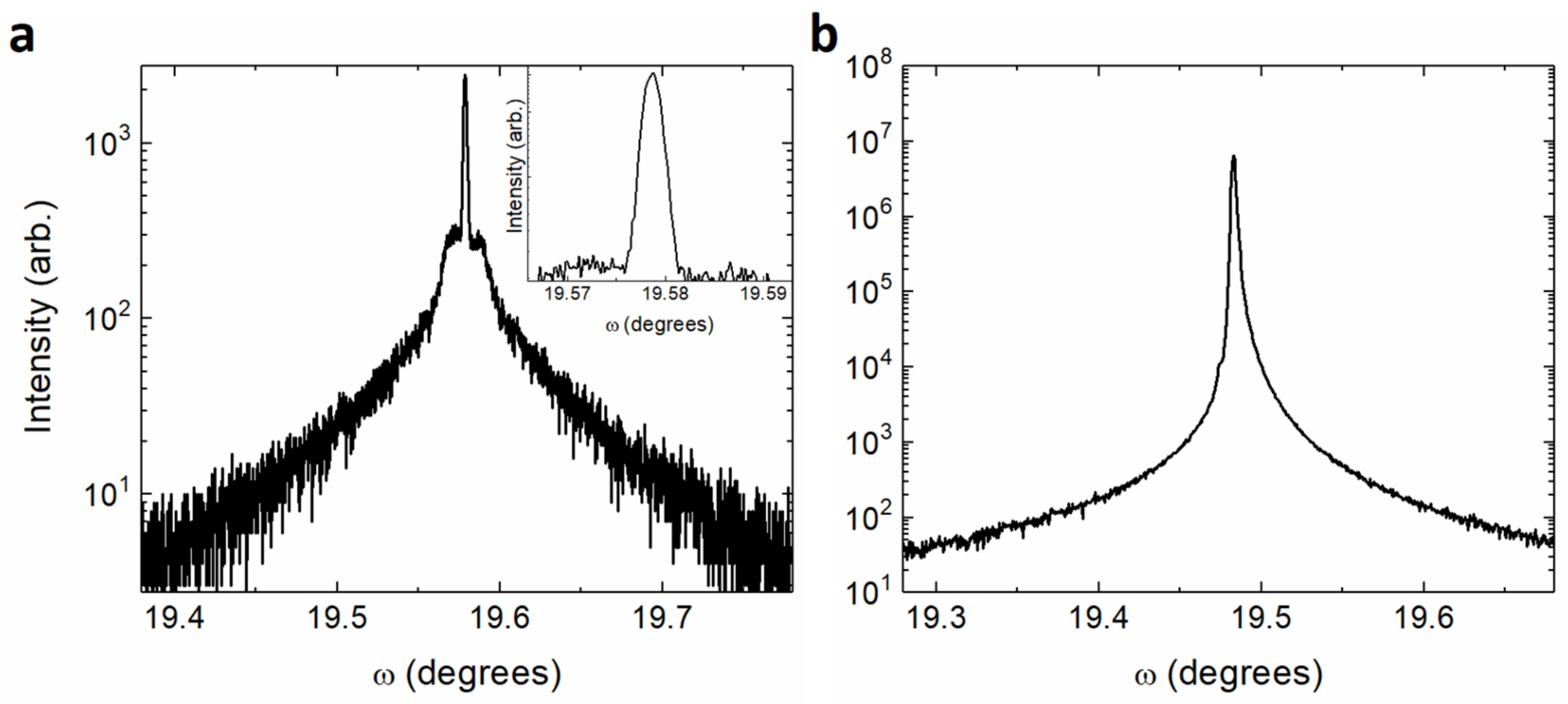
  77. Tellekamp, M.B.; Shank, J.C.; Goorsky, M.S.; Doolittle, W.A. Molecular Beam Epitaxy Growth of High Crystalline Quality LiNbO3. J. Electron. Mater. 2016, 45, 6292–6299. [Google Scholar] [CrossRef]
  78. Volk, T.; Wöhlecke, M. Lithium Niobate: Defects, Photorefraction and Ferroelectric Switching; Springer: Berlin/Heidelberg, Germany, 2008; Volume 115. [Google Scholar]
  79. Liu, D.; Zha, G.; Hu, L.; Jiang, W. Recovery of Gallium and Arsenic from Gallium Arsenide Semiconductor Scraps. In TMS Annual Meeting & Exhibition; Springer: Berlin/Heidelberg, Germany, 2018; pp. 319–330. [Google Scholar]
  80. Tellekamp, M.B.; Shank, J.C.; Doolittle, W.A. Molecular Beam Epitaxy of lithium niobium oxide multifunctional materials. J. Cryst. Growth 2017, 463, 156–161. [Google Scholar] [CrossRef] [Green Version]
  81. Zivasatienraj, B.; Tellekamp, M.B.; Weidenbach, A.S.; Ghosh, A.; McCrone, T.M.; Doolittle, W.A. Temporal versatility from intercalation-based neuromorphic devices exhibiting 150 mV non-volatile operation. J. Appl. Phys. 2020, 127, 084501. [Google Scholar] [CrossRef]
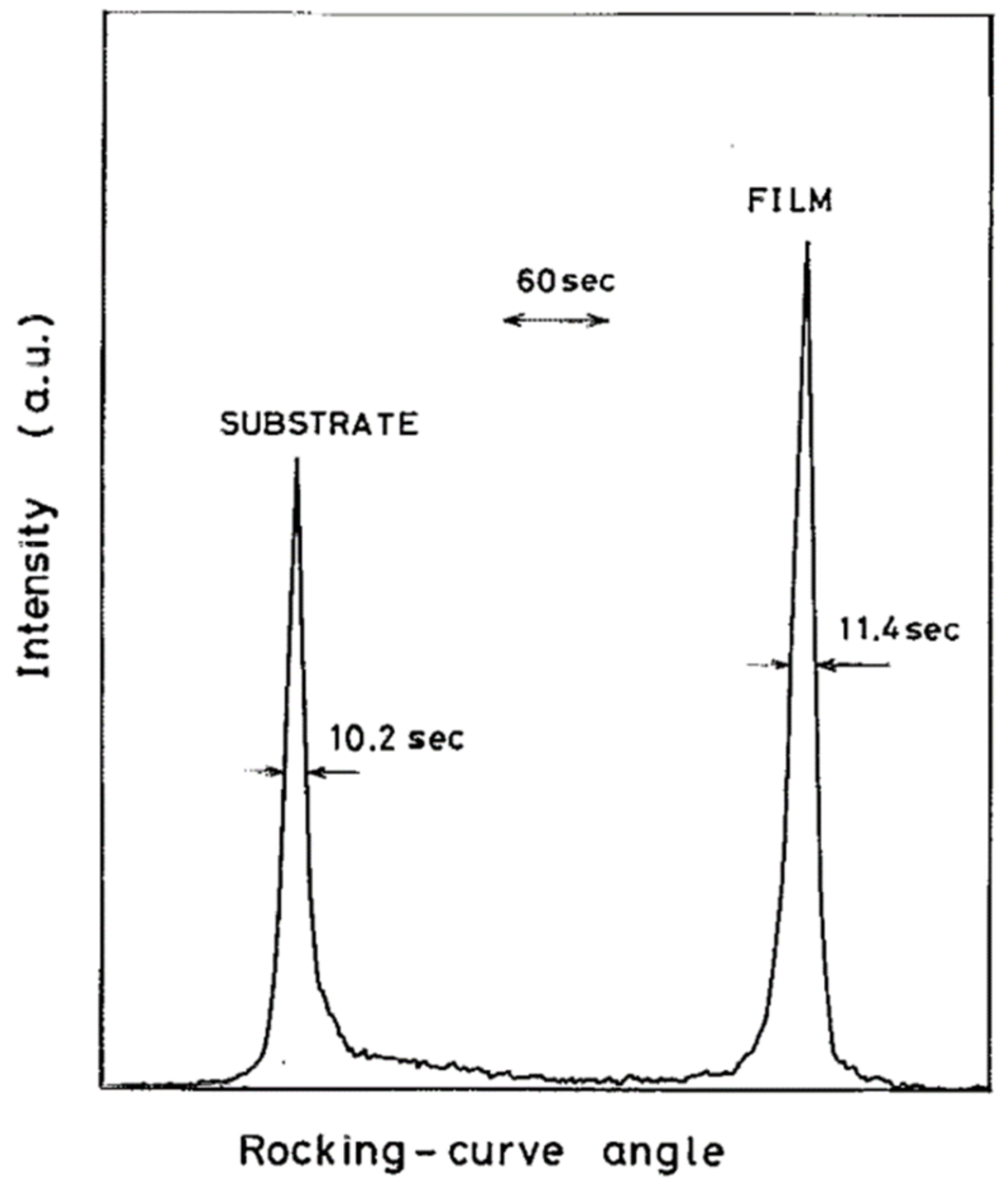
  82. Miyazawa, S. Growth of LiNbO3single-crystal film for optical waveguides. Appl. Phys. Lett. 1973, 23, 198–200. [Google Scholar] [CrossRef]
  83. Bartasyte, A.; Plausinaitiene, V.; Abrutis, A.; Stanionyte, S.; Margueron, S.; Boulet, P.; Kobata, T.; Uesu, Y.; Gleize, J. Identification of LiNbO3, LiNb3O8 and Li3NbO4 phases in thin films synthesized with different deposition techniques by means of XRD and Raman spectroscopy. J. Phys. Condens. Matter 2013, 25, 205901. [Google Scholar] [CrossRef]
  84. Astié, V.; Oliveri, S.; Millon, C.; Margueron, S.; Rachetti, M.; Decams, J.; Boulet, P.; Bartasyte, A. Towards stoichiometric LiNbO3 epitaxial thin films grown by DLI-MOCVD. In Proceedings of the GDR Oxydes Fonctionnels—des Matériaux Aux Dispositifs, Piriac sur Mer, France, 20–23 March 2018. [Google Scholar]
  85. Cho, A.Y. Morphology of Epitaxial Growth of GaAs by a Molecular Beam Method: The Observation of Surface Structures. J. Appl. Phys. 1970, 41, 2780–2786. [Google Scholar] [CrossRef]
  86. Cho, A.Y.; Panish, M.B.; Hayashi, I. Molecular beam epitaxy of GaAs, AlxGa1-xAs and GaP. Proc. Symp. GaAs Relat. Compd. 1970, 2, 18–29. [Google Scholar]
Figure 1. (a) X-ray diffraction rocking curve of epitaxial LN grown on sapphire via molecular beam epitaxy [77], with an 8.6 arcsec FWHM indicating a high-quality crystal strained to the sapphire substrate. The inset shows a well-resolved, narrow peak. (b) X-ray diffraction rocking curve of a bulk-grown LN wafer, with an FWHM of 10.4 arcsec.
Crystals 11 00397 g001
Figure 2. (a) The phase diagram of bulk LN adapted from Volk and Wohlecke [78] shows complex phase spaces and a narrow growth window for monophasic LN. The distinct lack of a convenient line composition creates many challenges, culminating in the need for finer control over the many growth parameters during LN epitaxy. (b) By comparison to LN, the phase diagram of bulk GaAs adapted from Liu et al. [79] shows that monophasic GaAs is grown, regardless of the growth ratio of As to Ga, ultimately making the epitaxial process less challenging.
Crystals 11 00397 g002
Figure 3. X-ray diffraction rocking curve with an FWHM of 11.4 arcseconds from a LN thin film grown in 1992 via liquid phase epitaxy (LPE) by Yamada et al. [23], juxtaposed with the MgO-doped LN substrate.
Crystals 11 00397 g003
Figure 4. A pseudo-phase diagram varying the Li and Nb feed composition with growth temperature that shows growth windows for single and multiple phase LN epitaxy via MOCVD by Akiyama et al. [49].
Crystals 11 00397 g004
Figure 5. Light injected into a LN thin film grown on sapphire via pulsed laser deposition (PLD) by Kilburger et al. [63,64] shows low propagation losses that indicate a high-quality crystalline film.
Crystals 11 00397 g005
Table 1. Comparison of optical loss and X-ray diffraction rocking curve full width at half maximum (FWHM) metrics for different epitaxial techniques as reported. Unless specified otherwise, optical losses are measured in the TE0 mode at wavelength λ = 632.8 nm.
Epitaxial TechniqueOptical Loss (dB/cm)XRD FWHM (Arcseconds)NotesReference
LPE5-20–30 dB/cm losses at visible wavelengths.Kondo et al. [20]
<5--Ballman et al. [18]
1.611Significant vanadium impurities. λ = 514.5 nm.Tamada et al. [22]
<111.4λ = 458 nm.Yamada et al. [23]
Sputter9--Takada et al. [28]
3-Amorphous film.Hewig et al. [30]
6.47--Shimizu et al. [36]
1.2648Multi-step process.Lansiaux et al. [39]
CVD-1368Twinning detected.Wernberg et al. [44]
1.836No twinning detected.Feigelson et al. [46]
PLD-612-Shibata et al. [56]
-360-Aubert et al. [59]
<1.5165.6-Kilburger et al. [64]
MBE15.7-Electron-beam evaporated sources.Betts and Pitt [66]
-13Twinning detected. Laser assisted.Matsubara et al. [70]
-104Metal–organic precursors.Dabirian et al. [73]
-8.6No twinning detected. Metal–halide sources.Tellekamp et al. [77]
Publisher’s Note: MDPI stays neutral with regard to jurisdictional claims in published maps and institutional affiliations.

