Article

Combinatorial Materials Design Approach to Investigate Adhesion Layer Chemistry for Optimal Interfacial Adhesion Strength

1
Empa, Swiss Federal Laboratories for Materials Science and Technology, Laboratory for Mechanics of Materials and Nanostructures, Feuerwerkerstrasse 39, 3602 Thun, Switzerland
2
Department of Metallurgical and Materials Engineering, Colorado School of Mines, 1500 Illinois St., Golden, CO 80401, USA
3
Materials Department, University of California, Santa Barbara, Engineering II Building, 1355, Santa Barbara, CA 93106, USA
4
Institute of Applied Laser, Photonics and Surface Technologies ALPS, BFH, Bern University of Applied Sciences, Quellgasse 21, 2502 Biel, Switzerland
*
Author to whom correspondence should be addressed.
Equally contributing.
Crystals 2021, 11(4), 357; https://doi.org/10.3390/cryst11040357
Submission received: 16 March 2021 / Revised: 23 March 2021 / Accepted: 26 March 2021 / Published: 30 March 2021
(This article belongs to the Special Issue Advanced Nanoindentation in Materials)

Abstract

:
A combinatorial material adhesion study was used to optimize the composition of an adhesion promoting layer for a nanocrystalline diamond (NCD) coating on silicon. Three different adhesion promoting metals, namely W, Cr, and Ta, were selected to fabricate arrays of co-sputtered binary alloy films, with patches of seven different, distinct alloy compositions for each combination, and single element reference films on a single Si wafer (three wafers in total; W–Cr, Cr–Ta, Ta–W). Scratch testing was used to determine the critical failure load and practical work of adhesion for the NCD coatings as a function of adhesion layer chemistry. All tested samples eventually exhibit delamination of the NCD coating, with buckles radiating perpendicularly away from the scratch track. Application of any of the presented adhesion layers yields an increase of the critical failure load for delamination as compared to NCD on Si. While the influence of adhesion layers on the maximum buckle length is less pronounced, shorter buckles are obtained with pure W and Cr–Ta alloy layers. As a general rule, the addition of an adhesion layer showed a 75% improvement in the measured adhesion energies of the NCD films compared to the NCD coating without an adhesion layer, with specific alloys and compositions showing up to 125% increase in calculated practical work of adhesion.

1. Introduction

The ability to design and realize materials with an optimum property profile is essential for the development of future technologies, promoting for instance the environment sparing use of resources or sustainable and efficient generation and use of energy [1,2,3]. Ideally, material discovery and design efforts involve close coupling between materials prediction, synthesis, and characterization [2]. Combinatorial thin film science is one optimization method for material properties, whether they be mechanical, functional, or interfacial, using significantly fewer resources than a traditional bulk analysis technique and conducted in substantially less time [4,5,6]. The method combines high-throughput synthesis and subsequent characterization of multinary material libraries on a single wafer, allowing for screening of unique properties or the optimization of specific properties for a desired application. Regarding fabrication of such libraries, physical vapor deposition (PVD) such as magnetron sputtering with different targets is a common technique, using either co-deposition [5,7,8,9,10,11] or wedge-deposited multilayered thickness gradients of different elements combined with post-deposition annealing treatments for alloying [3,6,12]. Thereby, programmable shutter systems incorporated into the sputter chamber allow the realization of wedge geometries [3,6,12], as well as 2D patterning of the alloys into discrete arrays, facilitating the subsequent characterization and categorization of properties based on their different chemical compositions.
This characterization of resulting material properties typically demands methods with adequate lateral resolution. It includes correlation of the chemical composition to the atomic structure and development of resulting structure-property relationships impacting e.g., formability [13], toughness [11], oxidation resistance [3] or interfacial adhesion [6]. The latter property is a critical factor for any thin film application, regardless of the specific coating application. From the variety of methods available to measure interfacial adhesion (overview found in [14,15]) only a few fulfill the combinatorial requirements of high spatial resolution, time efficiency and quantitative results. Recently, the potential of nanoindentation induced blisters for combinatorial adhesion studies has been demonstrated by the authors [6], with some compromises on quantification of the results.
Another adhesion method deemed suitable for this purpose is scratch testing [16,17,18,19,20,21,22]. It can be automated, relatively fast and small-scale. However, the analysis based on the nature of the generated scratch trace is rarely straightforward. Depending on the coating-substrate combination, different failure modes can occur, namely plastic deformation and extrusion of the coating (soft coatings/hard substrates) or coating fracture, spallation, and buckling (hard coatings/hard substrates) [17,19]. As a results, scratch testing is often used as a semi-quantitative or comparative adhesion test, based on the critical coating failure load, Lc. As long as the failure mode remains consistent across different samples and the point of failure can be determined, it is also possible to quantify scratch test results and determine the adhesion energy of the system. When quantifying the results, many intrinsic and extrinsic factors affecting the failure mode need to be considered. Certain intrinsic factors (e.g., loading rate, indenter tip radius, machine stiffness) can be kept constant for one given set of measurements, allowing for valid comparisons to be made between different systems. Similarly, the extrinsic factors relating to coating and substrate properties are measurable and can be incorporated into existing adhesion models [21]. In certain cases, quantitative analysis based on buckle geometry or spallation is also permitted [23,24].
In this work, we report the use of scratch testing to measure interfacial adhesion of nanocrystalline diamond coatings (NCD) as a function of combinatorially designed, adhesion promoting interlayers. NCD coatings can combine a very low surface roughness with the outstanding properties of diamond such as high hardness, wear and corrosion resistance, low self-friction coefficient, and biotolerance. This makes NCD coatings suitable for many applications and attractive to numerous industries [25,26]. However, depending on the type of substrate, they also exhibit a weak interface bonding strength, requiring the application of adhesion promoting interlayers [27,28,29]. Therefore, a unique shutter system allowing for precise control over coating design has been integrated into a conventional physical vapor deposition (PVD) system to produce a matrix of single element and co-sputtered binary metallic alloy compositions, based on established adhesion promoting elements (Ta, W, Cr) [24,30,31,32,33,34] on single Si wafers. The combination of individual elements offers the potential for further optimization of adhesive strength and an overall improved property profile. Based on comparisons of the observed NCD scratch behavior as a function of adhesion layer composition, recommendations and guidelines for interlayer design can be derived in a time- and resource-efficient manner.

2. Materials and Methods

2.1. Calculation of Practical Work of Adhesion from Critical Load

According to the Laugier model for scratch testing [21] the interfacial adhesion energy or practical work of adhesion is a combination of the intrinsic stress in the film, σ i n t ( x ) and the applied stress, σ a p p l ( x ) , needed to delaminate the coating from the substrate. Thereby, the variable x defines the position along the scratch trace on the thin film surface. The applied stress due to a sliding spherical contact that causes delamination of the coating during scratch testing can be described as [35]:
σ a p p l ( x ) = L c 2 π a 2 { ( 4 + ν s ) 3 π f 8 ( 1 2 ν s ) }
where Lc is the applied critical failure load, f is the coefficient of friction (COF) between the coating and the indenter tip, ν s is the Poisson ratio of the substrate, and a is the radius of the contact circle. This contact circle radius, a, is calculated using Hertzian contact theory:
a 3 =   3 4 L R ( 1 ν s 2 E s + 1 ν i 2 E i )
where R is the radius of curvature of the indenter, L is the applied load, ν s   and   ν i are the Poisson ratio of the substrate and indenter, respectively, and E s   and   E i are the Young’s modulus of the substrate and indenter, respectively. The elastic constants of the utilized Berkovich diamond indenter tip are: Ei = 1140 GPa and vi = 0.07 [36]. Regarding the elastic constants of the substrate, only contributions from the Si wafer were considered, with Es = 160 GPa and νs = 0.22 [37] for all calculations. While for single NCD films on Si this assumption is fully valid, the addition of an adhesion layer requires further considerations. It has been observed that in the bilayer systems (NCD + adhesion layer) delamination during scratch testing typically occurs at the NCD-adhesion layer interface. Therefore, the adhesion layers can be ascribed to the substrate side in terms of adhesion mechanics. However, due to their continuously varying elastic properties across the different bilayer systems, an inherent feature of the combinatorial design strategy, the simplification of only considering elastic properties of the Si substrate was introduced. Furthermore, based on the limited thickness of the utilized adhesion layers (~50 nm) they are assumed to not substantially affect the elastic properties of the Si substrate. The potential impact of this simplification will be discussed in detail in the discussion section of the manuscript.
Based on the applied stress at the critical load (Equation (1)), the work of adhesion, W, required to delaminate a coating (film thickness, h, Young’s modulus, Ec) from the substrate can be approximated by:
W = { σ a p p ( x ) } 2 2 E c h
assuming that the internal stress in the coating, σ i n t ( x ) is zero. This simplification of the adhesion model is adopted as the actual internal stress state in the NCD coatings is unknown. Assuming that this internal stress state is at least comparable between the different material systems (similar microstructure, further detailed in the discussion section), the induced error still allows for a relative comparison of adhesion energies. NCD coating thickness values, h, as a function of the different adhesion layers are summarized in the results section of the manuscript (Section 3.1). The modulus of the NCD coating was measured as Ec = 210 GPa from nanoindentation experiments. Since selective post-mortem cross-sectioning of the obtained buckles indicates delamination at the NCD-adhesion layer interface, the different adhesion layers do not require consideration in terms of relevant coating properties (h, Ec).
In summary, the adhesion values stated in this work, obtained from scratch testing with the above described simplified adhesion model, should be treated as qualitative indicators for better and worse interfacial adhesion, rather than absolute quantitative numbers.

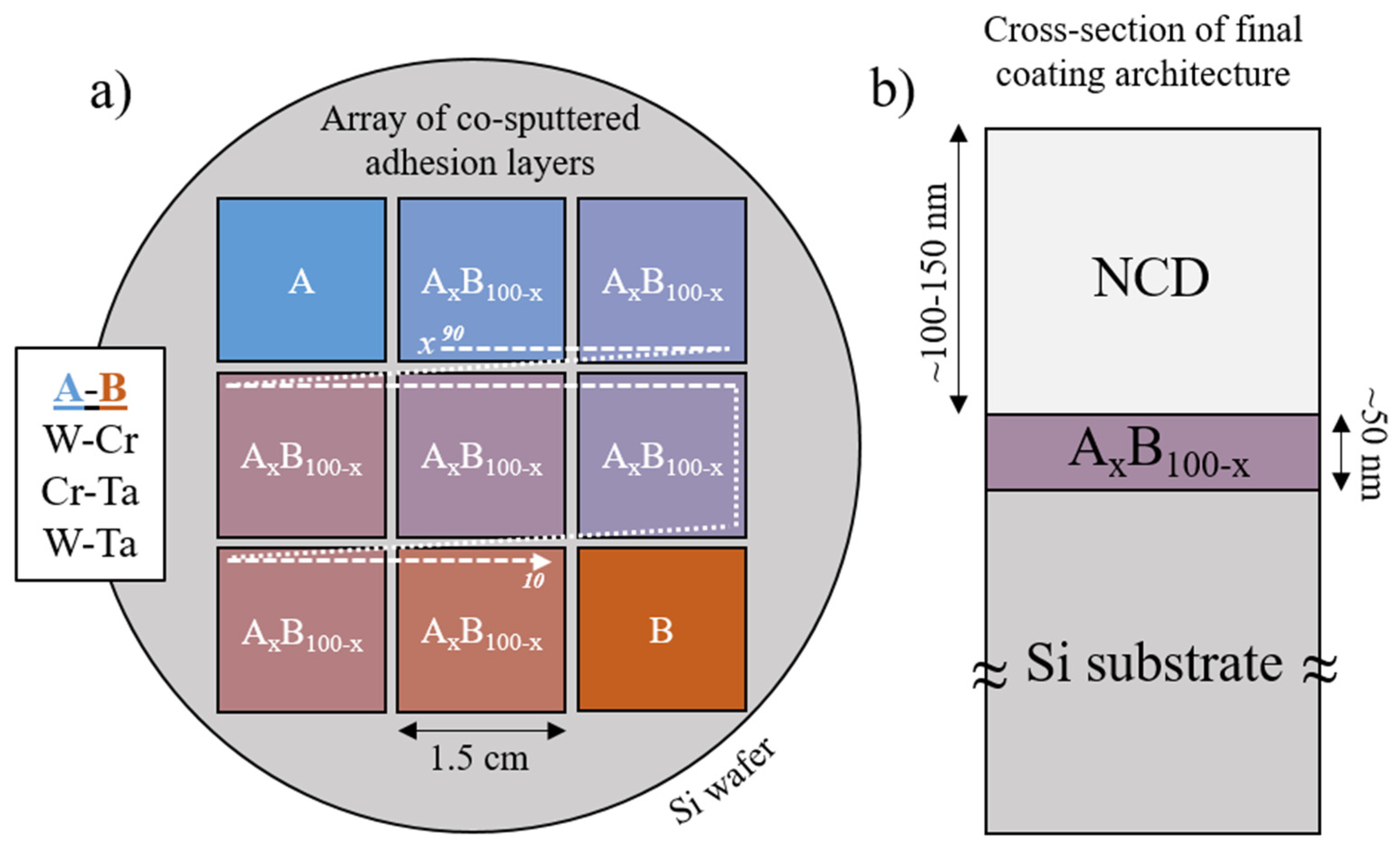
2.2. Experimental Details

A unique shutter control system allowing for precise control over coating design was integrated into a Mantis Deposition Ltd. QPrep physical vapor deposition (PVD) system with three magnetron sputtering targets for combinatorial synthesis of the adhesion layers. A detailed description of the shutter system can be found in Ref. [6]. A combination of W, Cr, and Ta was used to create (3 × 3) matrices of single element and binary alloy adhesion layers with different compositions on single 2” passivated Si wafers, schematically shown in Figure 1a. The movement of the shutter system required to form these specific matrix structures is shown in the supplementary video file S1.
Each 1.5 cm square in the 3 × 3 matrix (Figure 1a) was deposited using magnetron sputtering from elemental targets (W, Cr and Ta) at a base pressure of 3 × 10⁻⁵ Pa and a process pressure of 5 × 10⁻¹ Pa with 20 sccm Ar flow, to a thickness of approximately 50 nm. Binary adhesion layers were co-sputtered, whereby the power at each individual elemental target was adjusted for each square to vary their chemical composition, following pre-determined deposition recipes. For single element films only the respective target was active during deposition. The composition and thickness of each adhesion layer square, summarized in Table 1, were measured using X-ray fluorescence (XRF) on a Fischerscope X-ray XDV with a W source and accelerating voltage of 30 kV.
After deposition of the adhesion layers, a nanocrystalline diamond top coating (NCD, 110–150 nm thickness) was deposited (schematic cross-section of final bilayer architecture, Figure 1b). Therefore, each wafer containing the adhesion layers was first seeded at NeoCoat SA, using a proprietary process, by immersing the wafers in a liquid containing 10 nm diamond nanoparticles in suspension [38]. Previous investigations of the seeding density from this process on bare Si substrate showed an average cluster distance of 20 nm and surface coverage of approximately 66% [39]. Prior to NCD diamond deposition, all samples were exposed to pure H2 plasma with increasing microwave power for approximately 1 h. The NCD diamond was deposited using a Matrix Elementary Plasma Source [40] in a home-made Matrix Elementary Plasma Source (MEPS) system using four microwaves antennas, Hi-Wave applicators from SAIREM [41], positioned in a square configuration with an axis distance of 80 mm. The coating was deposited at a substrate temperature of 350 °C. The microwave power to sustain the plasma was delivered by 4 solid-state microwave generators (Sairem GMS 200), each coupled via a coaxial cable to a plasma source. The microwave power during the deposition process was 800 W total, 200 W per source. To obtain reproducible deposition conditions, the reflected power is reduced to a level below 5 W, by automatically, individually frequency tuning each generator. The process gas is a mixture of 6% CH4 in 94% H2, at a pressure of 50 Pa. Microstructure and thicknesses of the resulting NCD coatings were investigated with cross-sectional SEM (Hitachi S-4800) imaging and bright field scanning transmission electron microscopy (BF-STEM, JEOL 2200FS). The thickness values of the NCD films ranged between 110 and 150 nm, as summarized in the results section of the manuscript (Section 3.1) 3 Quasi-static nanoindentation was performed on a Hysitron UBI system equipped with a Berkovich diamond indenter to determine the Young’s modulus and hardness of the NCD films based on the Oliver-Pharr method [36]. The films were indented to a depth of 30 nm on areas without an adhesion layer (i.e., grown on top of bare silicon between the squares).
Scratch testing was performed at room temperature on a NanoIndenter XP system using a 2 µm radius conical diamond tip with a 120° opening angle. Three ramped load scratch tests (0–100 mN) were applied at a loading rate of 10 µm/s for 500 µm, with the peak load occurring after 432 µm. The scratch profiles were then imaged in a cold field emission scanning electron microscope (SEM, Hitachi S-4800) to determine the critical load, Lc, and maximum buckle length, Wb, for each adhesion layer compositions. Lc is defined as the load at which delamination/buckles are first observed at the scratch trace, Wb is the maximum distance those buckles propagate, perpendicular to the scratch trace. Typically, buckle formation or delamination also correspond to an abrupt variation in lateral force or friction coefficient during scratch testing. As the measurement of these two quantities was not permitted with the utilized setup, Lc had to be determined through post mortem visual SEM inspection of the scratch traces. Focused ion-beam (FIB, Tescan Lyra/XMU dual-beam) cross-sections at the onset of buckle formation were cut from three different compositions and imaged to determine the buckle geometries and delaminating interfaces.

3. Results

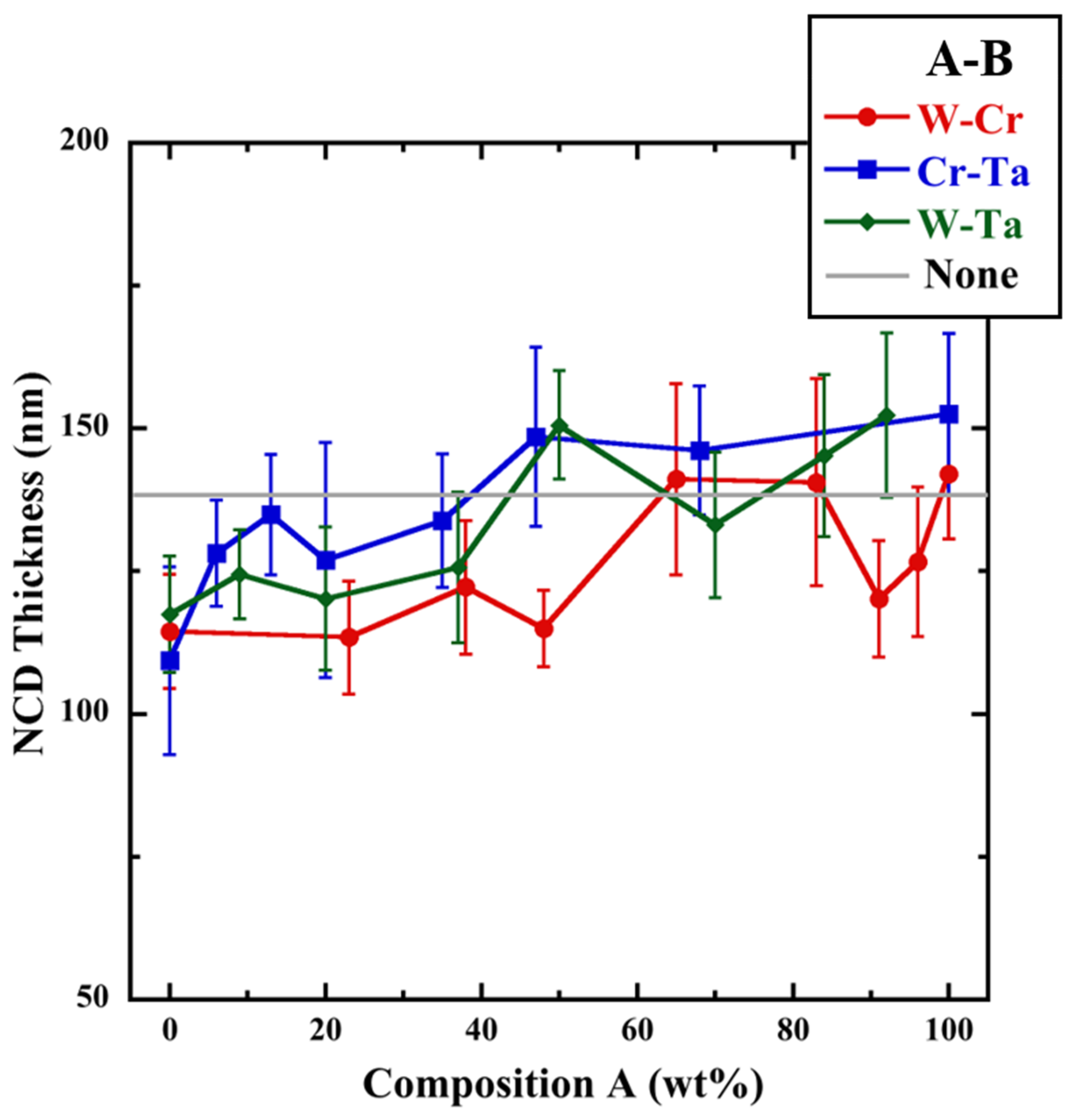
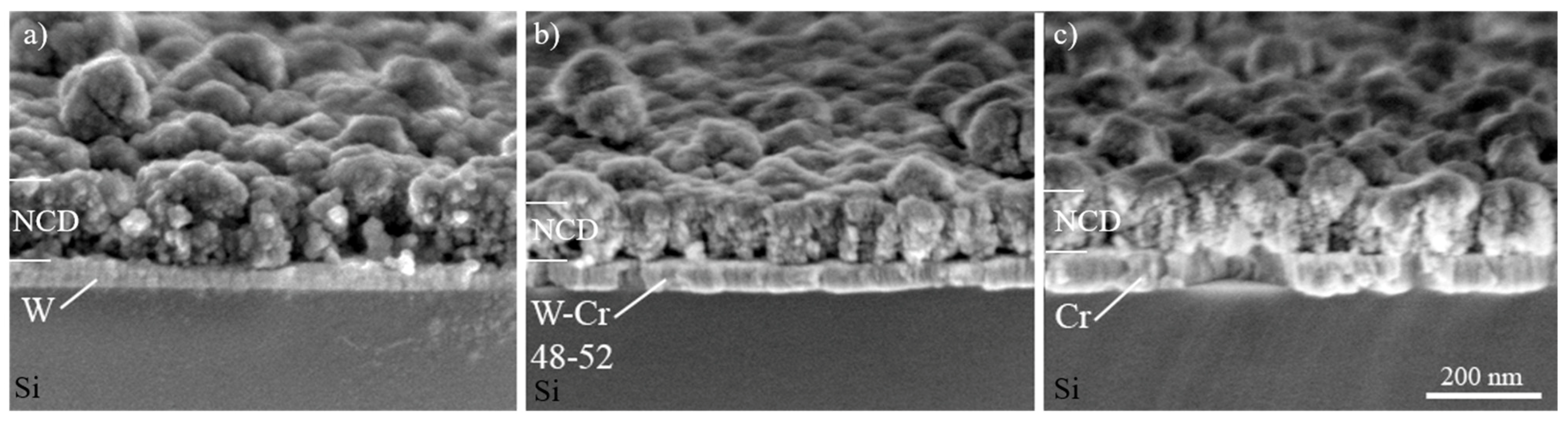
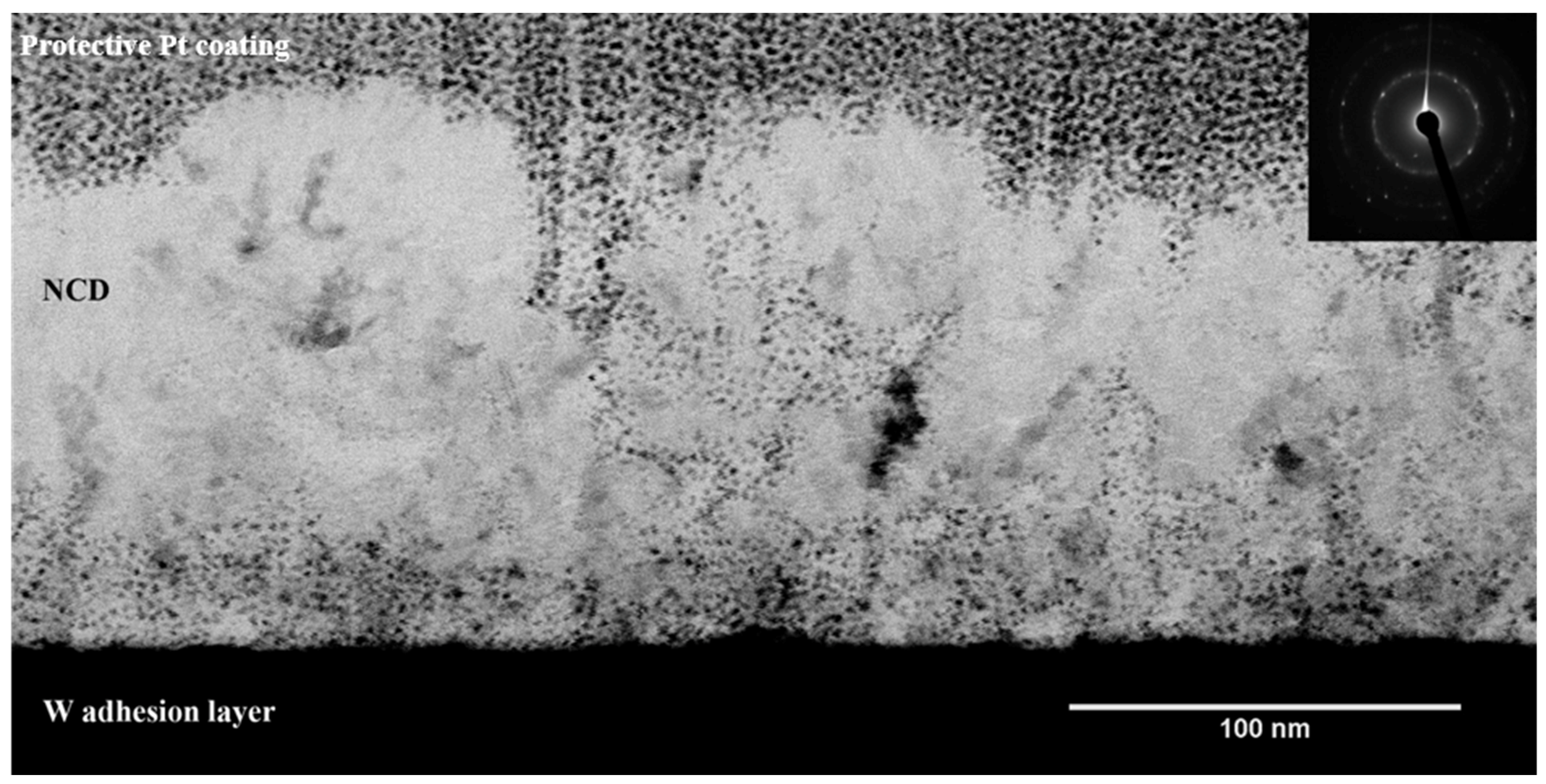
3.1. NCD Microstructure

Cross-sectional SEM images taken on cleaved sections of the samples showed a slight spatial or compositional dependence of NCD growth on the adhesion layer chemistry. Figure 2 shows these cleaved sections, imaged at 70°, for three different compositions of the binary adhesion layer system W–Cr: pure W, W–Cr alloy with composition 48–52 wt%, and pure Cr. The NCD coating thickness was measured to be 150 ± 16 nm, 120 ± 12 nm and 117 ± 14 nm for pure W, W–Cr, alloy and pure Cr, respectively. For comparison, on pure Ta (not pictured), the NCD coating thickness was measured as 120 ± 14 nm.
This variation of the NCD coating thickness as a function of adhesion layer composition is summarized in Figure 3, for all three binary material systems under investigation. The presented thickness values apply to the NCD layer only, and do not include the thickness of the underlying adhesion layer. For comparison, the NCD thickness measured on Si without adhesion layer (labelled “none”) is also included. For each binary alloy a similar moderate trend of an approximately linear thickness increase is observed as the concentration of element A (W or Cr depending on the alloy) increases. However, these variations in NCD growth rate and resulting film thickness across the wafers are most likely not directly related to the underlying adhesion layer chemistry. Instead, local variations of deposition conditions inside the NCD deposition chamber are thought responsible for causing the obtained variations in NCD thickness. Since the position of each adhesion layer square on a Si wafer (Figure 1a) corresponds to a specific position inside the NCD chamber during deposition as well as a specific change in adhesion layer composition and chemistry, it is difficult to unambiguously determine the underlying reasons for the different NCD growth rates. However, since the variation in NCD coating thickness is later accounted for in the adhesion energy model it does not affect the comparative analysis.
Aside from the thickness varying slightly across the samples, the microstructure of the NCD coating is consistent with clusters of smaller diamond grains, resembling a cauliflower-like structure, through the entire thickness of the coating (Figure 2). Such cauliflower-like morphology has been reported in literature for NCD coatings and MCD/NCD dual layer composites (MC = microcrystalline) [42,43]. No major inconsistencies of different grain or cluster sizes were observed across the different adhesion layer compositions. A substantial amount of porosity is observed in between the diamond grain clusters, and particularly at the bottom of the NCD films, close to the NCD- adhesion layer interface, as can be seen in both cross-sectional SEM (Figure 2) and bright field STEM images (Figure 4).
The representative bright field STEM (BF-STEM) image in Figure 4 shows a cross-section of an NCD coating on a pure W adhesion layer (Figure 4). It is clearly visible that the originally open, porous structure of the NCD coating has been progressively filled up with Pt-C during the TEM lift-out sample preparation process. The focused electron beam deposited Pt-C layer, used to protect the coating surface during the lift-out preparation, is clearly visible at the top of the TEM image with a distinctly dark, speckled contrast. The fact that this Pt-C deposit is also observed in the interior of the NCD coating and particularly at the interface to the adhesion layer (similar speckled contrast) indicates diffusion paths for the organometallic Pt-C precursor. Furthermore, the BF-STEM image also shows clusters of small crystalline diamond grains, approximately 10 nm in diameter. The flat surface of the W layer confirms that a smooth and uniform deposition of the adhesion layers was achieved with the integrated shutter system for composition control. The selected area diffraction (SAD) pattern included in Figure 4 (top right corner) further demonstrates the nanocrystalline nature of the diamond coating. The rings of diffracted spots seen in the pattern correspond to the {111}, {200} and {220} reflections of diamond, the uniform distribution of intensity within the rings indicates that the NCD has an equiaxed structure, at least at this length-scale.
The substantial porosity of the NCD coating can negatively affect the elastic modulus, which is an important parameter in the calculated work of adhesion using the present model. Porosity appears to be a result of the chosen NCD growth process, and is independent of the substrate or adhesion layer chemistry, based on cross-sectional SEM and TEM analyses. Therefore, the average elastic modulus and hardness of the NCD films without adhesion layers, measured with nanoindentation as 210 GPa and 11 GPa, respectively, indicate a relative density of ρ* = 0.45 according to the relationship:
E * E D ( ρ * ρ D ) 2
where E* and ρ* are the measured Young’s modulus and relative density of the porous NCD coating, respectively (E* equal to Ec in Equation (3)) and ED = 1050 GPa [44] is the Young’s modulus of diamond with a relative density of ρD = 1.

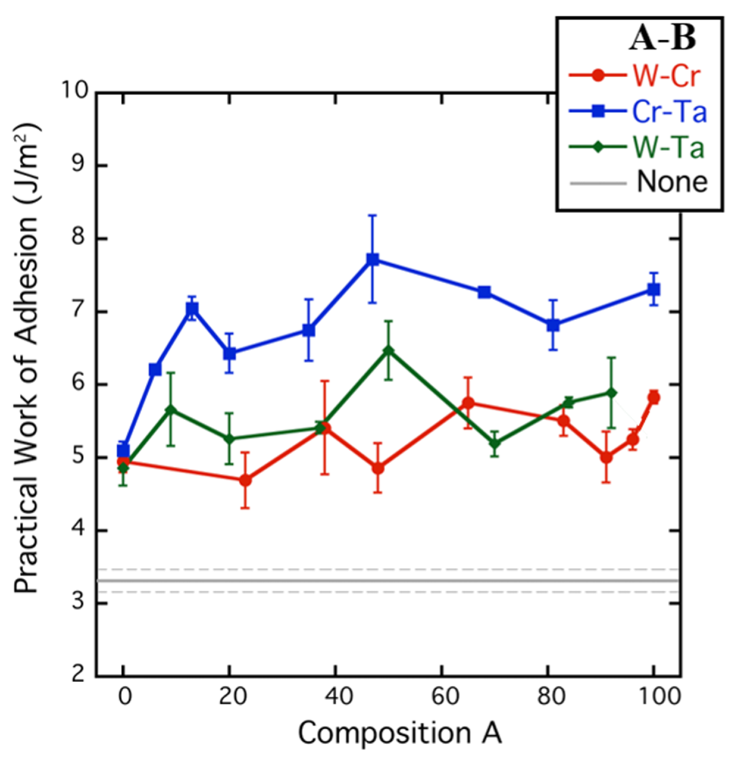
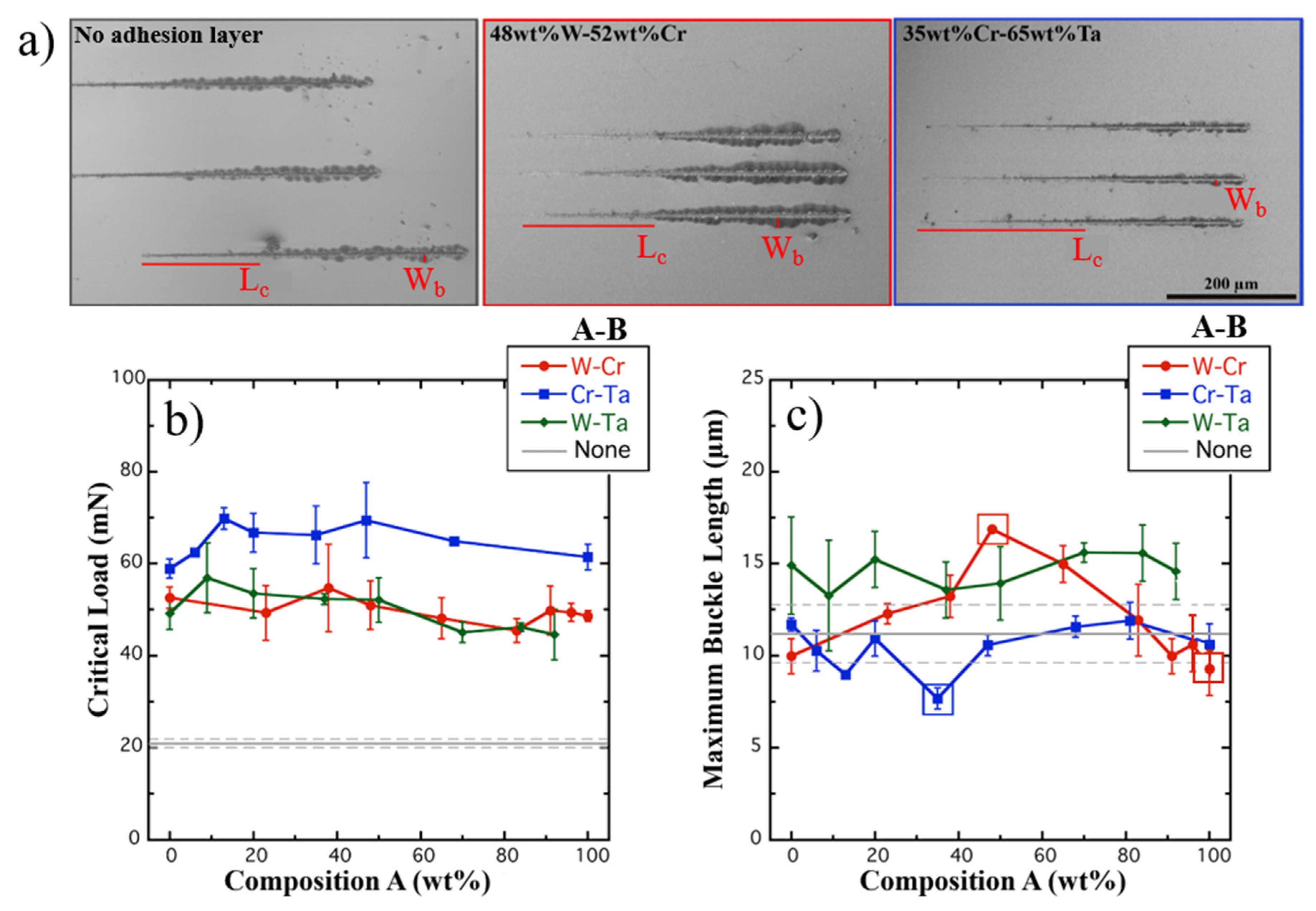
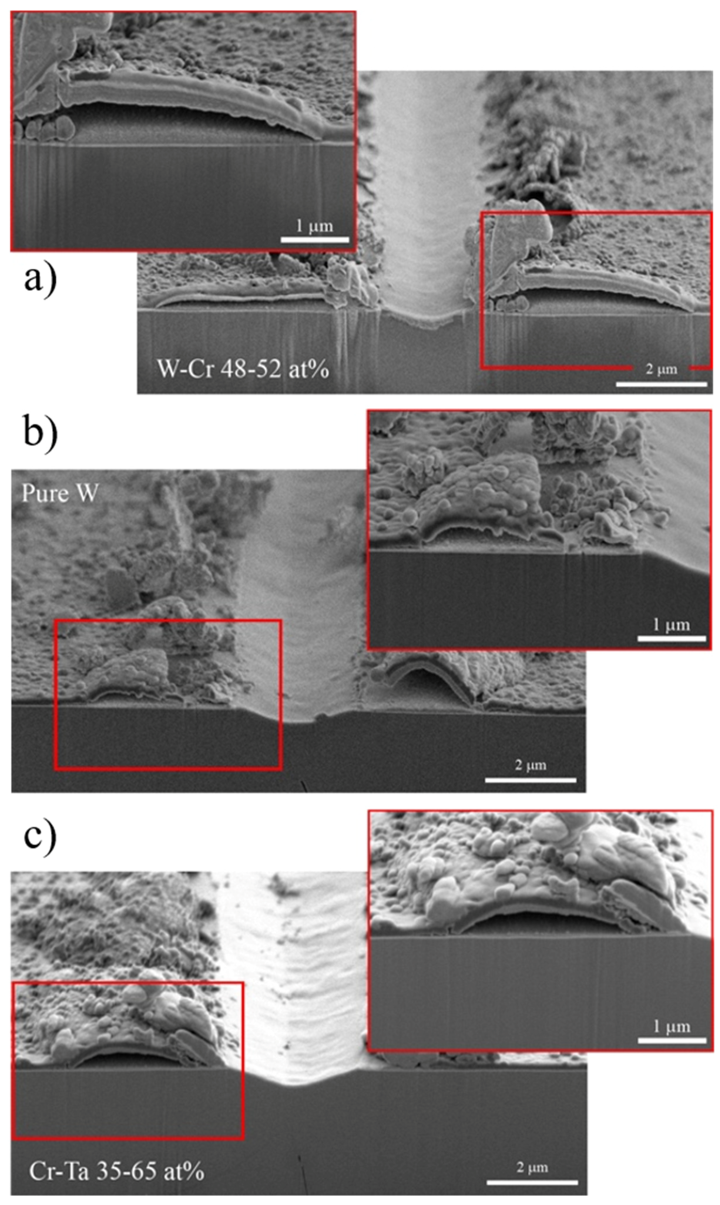
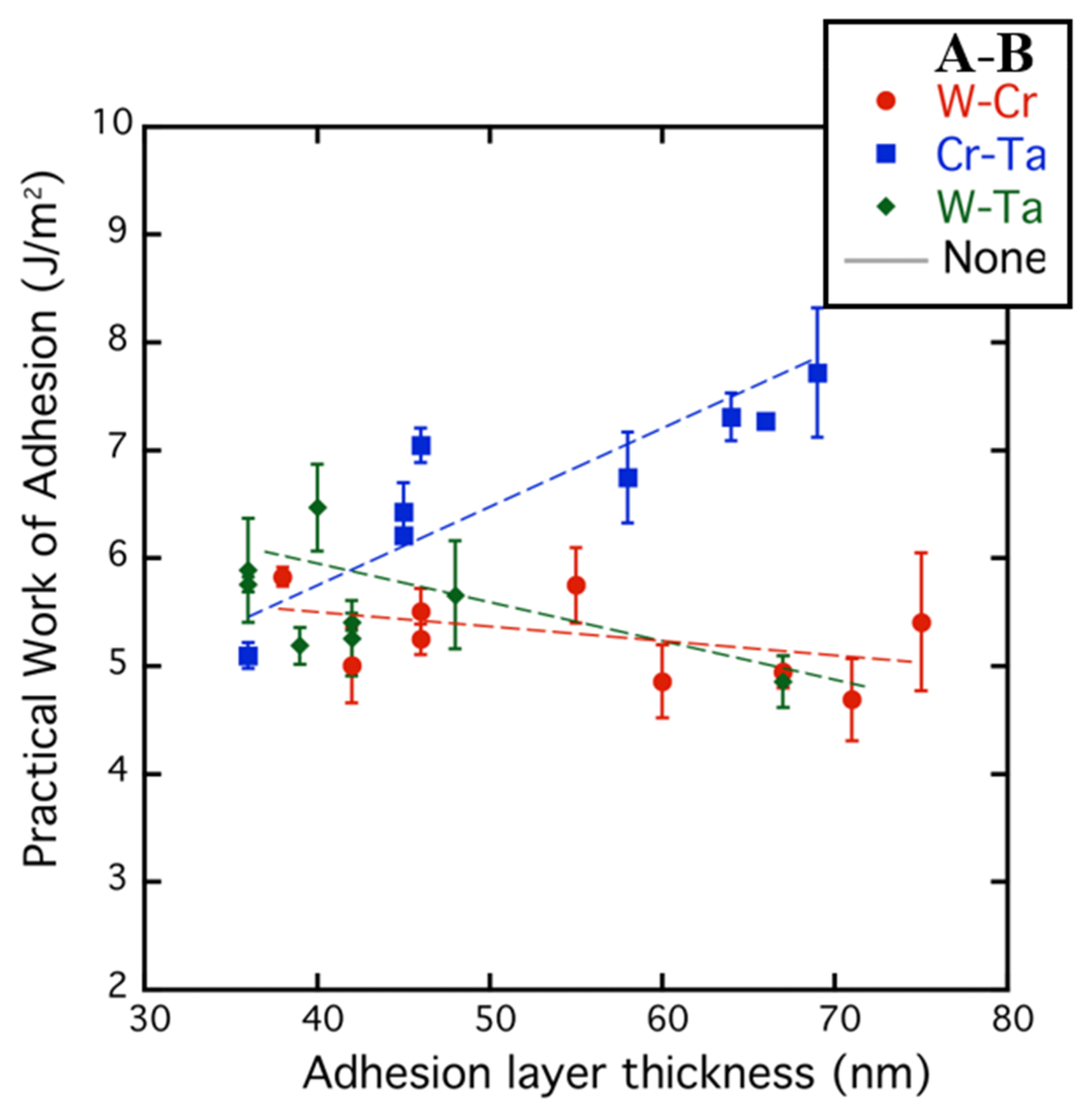
3.2. Scratch Testing: Critical Load and Buckle Length

The adhesion strength of the NCD coatings as a function of the different adhesion layer composition was evaluated using the scratch test method. Thereby, the experimentally determined critical failure load can be directly related to the adhesion energy of the system. In the presented film systems, the coatings failed by scratch-induced delamination in the form of buckles, radiating perpendicularly away from the scratch trench. Depending on the composition of the adhesion layer, these buckles are first observed at different critical failure loads, Lc, and propagate until reaching a maximum buckle length, Wb, referring to the distance of the edge of the scratch track to the edge of the largest buckle. The two quantities Lc and Wb were determined from SEM micrographs, as indicated in Figure 5a. The representative SEM images in Figure 5a show the scratch tracks obtained for an NCD film without adhesion layer and for NCD with two different adhesion layer compositions. Within one thin film system, three consecutively performed scratch tests yield a very similar response (same appearance of the scratch track). This indicates a good lateral homogeneity of the films and interfaces, despite the absence of substrate rotation during deposition which was prevented by the utilized shutter system, and a good reproducibility of the test method. Individual scratch traces are placed far enough apart in order not to influence each other (depending on Wb, min. 60 μm). Even at a quick glance, differences in the scratch response between the three film systems shown in Figure 5a are noticeable.
Figure 5b,c summarize the critical failure load, Lc, and the maximum buckle length, Wb, as a function of all investigated adhesion layer compositions. Particularly noticeable in Figure 5b is the increase of the critical failure load Lc in all of the samples with an adhesion layer when compared to the NCD grown directly on passivated Si (grey lines labeled as "None"). Among the three adhesion layers Cr–Ta exhibits the highest Lc values across the entire composition range. Furthermore, Cr additions of more than 10 wt% seem to slightly increase Lc as compared to pure Ta. For W–Cr and W–Ta very similar, generally lower Lc values are obtained, which remain, considering error bar, more or less constant over the whole compositional range, indicating no substantial benefit of alloying as compared to the single element adhesion layers. Regarding the maximum buckle length (Figure 5c), general trends as a function of adhesion layer composition are less straightforward. Consistent with higher critical loads, shorter buckles are observed for the Cr–Ta alloys and also for pure W adhesion layers (100 wt% Composition A, W–Cr and W–Ta).
Since adhesion energies are determined from the critical load at the first buckle formation Lc, three characteristic buckles were FIB cross-sectioned to determine the failing/delaminating interfaces. The adhesion layer compositions for cross-sectioning were chosen in order to represent three specific cases within the investigated spectrum of adhesive properties: (i) a low critical load and the largest maximum buckle length (poorest adhesion, 48 wt%W-52 wt%Cr), (ii) a low critical load but a shorter maximum buckle length (potentially better adhesion, even though not reflected in the calculation of adhesion enery, pure W) and (iii) the smallest maximum buckle length and largest critical load (best adhesion, 35 wt%Cr-65wt%Ta). These three compositions are also highlighted with squares in Figure 5c. Importantly, the SEM cross-sections presented in Figure 6 show that in all three cases delamination occurs at the interface between the NCD coating and the adhesion layer. The sample with the poorest interfacial adhesion (W–Cr adhesion layer, Figure 6a) shows flat buckle geometries with a large ratio of buckle height to length, which generally indicates that interfacial cracking can propagate easily. For the two other adhesion layer compositions (Figure 6b,c), the buckle geometries are quite similar with a smaller buckle height to length ratio and fracture of the NCD coating at the edges of the buckles, both of which indicate generally better adhesion as compared to the W–Cr sample.

4. Discussion

Scratch testing is best used as a qualitative measure of adhesion, mainly for determining a comparative improvement in adhesion for a set system. Traditionally this technique is used as a pass/fail criteria for industrial coatings, based on specifying critical loads at which cracking and spalling can occur. Actual adhesion values are rarely assigned to the measurements due to the extremely complicated stress state applied during the scratch process. Furthermore, the method is highly dependent on both substrate and coating properties. Some adhesion models exist for scratch testing of hard coatings on hard substrates, but are related to and dependent on a specific failure mode of the coating. Since the NCD coatings investigated in this work do not fail by spallation, any model requiring a measurement of the spalled region cannot be used [23]. Even though buckling has been observed, these specific types of parallel buckles are not suitable for existing adhesion models [24,45]. In contrast to spontaneous buckles growing away from the scratch trace, their formation parallel to scratch trace is due to a combination of many different deformation mechanisms.
Therefore, a more simplistic model developed by Laugier [21] was used to quantify the previously discussed scratch results based on the critical failure load. Since the NCD coating microstructure and properties do not change by a large amount as the adhesion layer composition changes, a comparison between the different cases is principally permitted. However, as outlined in Section 2.1 of the manuscript, several further simplifications and assumptions had to be made to the existing model to account for unknown parameters and inevitably changing properties of the adhesion layers. The impact of these assumptions will be discussed in detail in the following paragraphs. As a results, readers are encouraged to interpret the stated adhesion energies as qualitative comparisons, rather than absolute quantitative numbers. Figure 7 summarizes the work of adhesion values calculated using the simplified Laugier model as a function of adhesion layer composition and compared to the NCD coating deposited on the bare Si wafer (grey line, labeled ‘none’). Despite numerous simplifications, the obtained adhesion energies appear to be a reasonable order of magnitude [46].
Since scratch testing is highly dependent on the morphology of each surface, and on the coefficient of friction (COF) value between the two bodies (thin film and indenter tip) [18,22], it is important to use an appropriate value when attempting to quantify the adhesion energy (Equation (1)). In the case of these NCD films, the cauliflower-like microstructure leads to roughness values (Ra) of around 20 nm. A study conducted by Hayward et al. [47] specifically measured the effect of CVD diamond coating roughness on the COF values, with values ranging from 0.05 to 0.5 for coatings with roughness values of 2 nm and 200 nm, respectively. Based on the reported correlation between wear track roughness and friction coefficient (Figure 4 of Ref [47]) a COF of f = 0.18 is assumed for a coating with approximately Ra = 20 nm, as actual measurement of the COF vs. time curves was not permitted with the utilized scratch setup. A point of contention here is that for NCD films, which have a large fraction of atoms at the grain boundaries containing disordered sp²-hybridized carbon atoms, hydrocarbons and impurities [48], COF values can be significantly different and not comparable to high-quality diamond films [47]. In any case, the COF of our NCD coatings likely does not change as a function of adhesion layer chemistry since the microstructure is consistent across the different samples. Therefore, the error generated by the differences between actual and assumed COF affects all adhesion measurements equally (Equation (1)), thus still allowing for relative comparisons.
In general, the work of adhesion (Figure 7) is improved by the addition of any adhesion layer, with all samples showing at least a 50% improvement over the NCD coatings with no adhesion layer. In particular, the majority of the Cr–Ta alloy compositions show at least a factor of two improvement in the work of adhesion, consistent with their higher critical loads (Figure 5b). In previous adhesion studies, an apparent increase in the adhesion of hard coatings was observed in systems with a more compliant substrate or adhesion layer, due to the ability of these layers to plastically deform and absorb some of the energy [49]. Similarly, brittle films have been shown to propagate interfacial cracks [32] and can thus actually lead to reduced coating performance. While Cr–Ta alloy is not known as a ductile material, it is possible that it is less brittle than the W–Ta and W–Cr alloys, or that the Cr2Ta phase (laves phase), which is located in the 35–38 at% Ta region of the phase diagram, contributes to significant toughening of the adhesion layer [50]. Figure 7 also indicates that the adhesion energy obtained for the pure Cr interlayer is very different between the W–Cr and the Cr–Ta system, while for the other single element areas the values compare relatively well to one another. Since the thickness of pure Cr is also similar in both cases (67 nm vs. 64 nm, Table 1), the observed differences between the two adhesion layer patches are most likely due to their respective position in NCD chamber, as they are located on opposite ends of the adhesion layer arrays. The influence of adhesion layer thickness will be further discussed in Figure 8.
The simplified adhesion model presented in Section 2.1 makes a number of assumptions that need to be addressed:
Firstly, the model in general does not take into account multiple layers but rather assumes a single coating on an infinite substrate. However, in the current study there is the main coating of interest, the NCD (120–150 nm), as well as the underlying adhesion layer (35–75 nm) which results in two different interfaces as well as two different coating properties to incorporate into the model. The thickness of the interlayers is between 20–35 % of the total coating thickness. Even though it proves impossible to cross-section a buckle in every single scratch trace, there is evidence that delamination in the investigated systems predominantly occurs at the NCD-adhesion layer interface (Figure 6). Therefore, ignoring the effect of the adhesion layers while calculating the practical work of adhesion with the Laugier model is justified to some extent. However, a closer look at the work of adhesion values as a function of adhesion layer thickness indicates a potentially interesting trend (Figure 8). This variation of adhesion layer thickness is an unintended result of modulating sputter power and chemical composition for individual adhesion layer squares (Figure 1a), which also slightly influenced the deposition rates.
For the Cr–Ta system, a strong positive correlation between the work of adhesion and the adhesion layer thickness is observed. However, there is no correlation for the W–Cr case, and potentially a slightly negative trend with increasing thickness for W–Ta. Since it is not possible to de-convolute the effect of adhesion layer thickness and composition for this particular study, it is unclear if the increased adhesion energy observed with Cr–Ta is due to a change in the adhesion layer composition, the layer thickness, or a combination of both effects. While it is not possible to determine the extent of the effect adhesion layer thickness has on the adhesion energy calculation, the results do exemplify why this combinatorial method is such an important method for rapid investigations to improve upon the adhesion promoting capabilities of the system.
Secondly, the effect of internal stresses in both the NCD coating as well as the adhesion layer have been ignored for this study. Although the internal stress of the NCD coatings was not measured, one could imagine that under the employed deposition conditions, the NCD films do not have a large build-up of stress, as their significant porosity could allow for stress relaxation of the coating as a whole. However, it is also well known that in very porous thin films intrinsic tensile stress may arise due to interatomic forces across the under-dense regions [51,52]. Typically, tensile residual stresses are associated with coating fragmentation, while compressive residual stresses facilitate buckling and delamination [53]. A substantial amount of internal stress could therefore lead to delamination at lower (or higher) critical loads [54], since the work required to delaminate the coating is a combination of the applied stress and internal stress in the coating [21]. To clarify that point, a more detailed investigation of NCD films stresses would be required. However, since microstructure and porosity of the NCD films are consistent throughout the different material combinations, one can at least assume their stress states to be comparable. Therefore, the error introduced by neglecting intrinsic NCD stresses still allows for relative comparison between the different adhesion layers. The effect of any internal stresses in the adhesion layers themselves was also not considered and can likely have a profound effect on the results, even though they are considered as part of the substrate from a delamination point of view and therefore would not directly enter into the adhesion calculation (Equation (3)). In addition to chemical composition and thickness, different residual stress states in the adhesion layers can affect the mechanical behavior and associated absorption of energy at a certain applied load, thereby influencing the critical coating failure load during scratch testing. Due to the limited thickness of the adhesion layers, characterization of internal stresses was not permitted, thus making it impossible to infer the magnitude of the effect on adhesion energy.
Besides the potential influence of NCD porosity on residual coating stresses, significant porosity at the NCD-adhesion layer interface (Figure 4) can directly impact coating adhesion. Interface porosity is mainly a result of the chosen deposition parameters and was observed for all NCD coatings, independent of adhesion layer composition. Compared to a homogeneous and dense interface structure, the interface porosity could facilitate crack propagation along the interface and contribute to the consistently observed delamination behavior at the NCD-adhesion layer interface. In comparison, the delamination behavior of dense Al2O3 on combinatorial adhesion layers changes as a function of adhesion layer chemistry, resulting in a change of the delaminating interface across the wafer [6]. When comparing the obtained adhesion energy values to industrially relevant applications, interface roughness of both the NCD coating to adhesion layer as well as the adhesion layer to Si substrate need to be considered. It is well documented that increased interface roughness increases the practical adhesion of a coating to the substrate [55,56,57], so the atomically smooth silicon wafer used as a substrate in this investigation will give lower values of adhesion energy than if the same experiment were repeated on an engineering substrate.
Another important discussion point is the possible formation of carbides in the adhesion layers during NCD deposition, which can significantly alter their ductility and mechanical properties. All of the refractory metals used as combinatorial interlayers (Ta, W, Cr) form stable carbides in the presence of carbon or hydrocarbons [58,59]. However, due to the high carbide stability and the low solubility of carbon in these metals, no carbon diffusion into the volume of interlayer is expected at the modest deposition temperature of 350 °C. Instead, an intermediate carbide surface layers forms, whereby the layer growth rate is influenced mainly by the substrate temperature, the carbon concentration and diffusion coefficient in the particular carbide. Diamond nucleation starts readily after the adhesion layer surface is carburized [58]. Cross-sectional SEM and TEM analysis did not reveal carbide layers of significant thickness on the surface of the adhesion layers. Therefore, carbide formation is considered to be negligible in this case.
Ultimately, the presented combinatorial adhesion method provides a fast and useful comparison between adhesion promoting layers, even if it is nontrivial to isolate specific contributions of individual parameters or quantify a specific value for interfacial adhesion. Even though in this particular case no direct benefit of binary adhesion layers compared to their single element counterparts has been observed in terms of critical failure load, the evolution of the maximum buckle length does indicate potential beneficial and harmful alloy compositions. Furthermore, alloying allows for adaptation of the interlayers to specific processing or application requirements or design and improve their overall property profile, combining i.e., adhesion promotion with thermal stability, low diffusivity or specific optical properties in the case of transparent top coatings.

5. Conclusions

A combinatorial material design method was utilized to help facilitate a quick and efficient way of testing different compositions of an adhesion-promoting layer for a nanocrystalline diamond (NCD) coating on a silicon substrate. Seven different binary compositions together with their single element counterparts were deposited for each material combination (W–Ta, W–Cr, and Cr–Ta), followed by MEPS-NCD deposition and scratch testing to compare the relative adhesion strengths of the resulting bilayer thin films. In general, the addition of any adhesion layer showed a 75% improvement in the practical work of adhesion compared to the NCD coating without an adhesion layer and consistently, delamination was observed at the NCD-adhesion layer interface. Among the tested alloys, the majority of Cr–Ta compositions exhibit the highest critical failure loads and shortest buckle lengths during scratch testing, equating to improved interfacial adhesion. In summary, scratch testing has been proven to be a valuable analysis method and alternative to nanoindentation for combinatorial adhesion studies. While it remains challenging to quantify adhesion, the method is more versatile in terms of observed failure morphologies suitable to evaluate and compare adhesion energies over a wide range of different materials systems and direct subsequent detailed analysis towards an overall improved property profile.

Supplementary Materials

The following are available online at https://www.mdpi.com/article/10.3390/cryst11040357/s1, Video S1: Movement of the shutter system producing a 2D array of adhesion layers.

Author Contributions

Conceptualization, A.A.T., T.N., and J.M.; methodology, R.L.S., A.A.T., L.P., K.T., and O.A.; investigation, R.L.S., A.A.T., K.T., and L.P.; formal analysis, R.L.S., B.P., and A.A.T.; resources, T.N. and J.M.; writing—original draft preparation, R.L.S. and B.P.; writing—review and editing, all authors; visualization, R.L.S., B.P., and A.A.T.; supervision, T.N. and J.M.; funding acquisition, R.L.S., A.A.T., B.P., J.M., and T.N. All authors have read and agreed to the published version of the manuscript.

Funding

This work has been financially supported by the Swiss Federal Commission for Technology and Innovation (CTI) project 16867.2PFNM-NM. Further funding was obtained from the Empa Postdoc program co-funded by FP7: Marie Curie Actions (R.L.S. and A.A.T.) and the EMPAPOSTDOCS-II program (B.P.), which received funding from the European Union’s Horizon 2020 research and innovation program under the Marie Skłodowska-Curie grant agreement number 754364.

Institutional Review Board Statement

Not applicable.

Informed Consent Statement

Not applicable.

Data Availability Statement

The data presented in this study are available on request from the corresponding author. The data are not publicly available due to technical or time limitations.

Conflicts of Interest

The authors declare no conflict of interest.

References

  1. Ludwig, A. Discovery of new materials using combinatorial synthesis and high-throughput characterization of thin-film materials libraries combined with computational methods. NPJ Comput. Mater. 2019, 5. [Google Scholar] [CrossRef]
  2. Alberi, K.; Nardelli, M.B.; Zakutayev, A.; Mitas, L.; Curtarolo, S.; Jain, A.; Fornari, M. The 2019 materials by design roadmap. J. Photochem. Photobiol. A Chem. 2019, 52. [Google Scholar] [CrossRef]
  3. Naujoks, D.; Weiser, M.; Salomon, S.; Stein, H.; Virtanen, S.; Ludwig, A. Combinatorial Study on Phase Formation and Oxidation in the Thin Film Superalloy Subsystems Co–Al–Cr and Co–Al–Cr–W. ACS Comb. Sci. 2018, 20, 611–620. [Google Scholar] [CrossRef] [PubMed]
  4. Liu, J.; Liu, Y.; Gong, P.; Li, Y.; Moore, K.M.; Scanley, E.; Walker, F.; Broadbridge, C.C.; Schroers, J. Combinatorial exploration of color in gold-based alloys. Gold Bull. 2015, 48, 111–118. [Google Scholar] [CrossRef] [Green Version]
  5. Xiang, X. Combinatorial material synthesis and screening: An integrated materials chip approach to discovery and optimization of functional materials. Annu. Rev. Mater. Sci. 1999, 29, 149–171. [Google Scholar] [CrossRef]
  6. Schoeppner, R.; Ferguson, C.; Pethö, L.; Guerra-Nuñez, C.; Taylor, A.A.; Polyakov, M.; Putz, B.; Breguet, J.-M.; Utke, I.; Michler, J. Interfacial adhesion of alumina thin films over the full compositional range of ternary fcc alloy films: A combinatorial nanoindentation study. Mater. Des. 2020, 193. [Google Scholar] [CrossRef]
  7. Maier, W.F.; Stowe, K.; Sieg, S. Combinatorial and high-throughput materials science. Angew. Chem. Int. Ed. 2007, 46, 6016–6067. [Google Scholar] [CrossRef]
  8. Furrer, A.; Spolenak, R. Colors of thin films of binary and ternary gold- and platinum-based alloys. Acta Mater. 2014, 66, 241–250. [Google Scholar] [CrossRef]
  9. Guerin, S.; Hayden, B.E. Physical vapor deposition method for the high-throughput synthesis of solid-state material libraries. J. Comb. Chem. 2006, 8, 66–73. [Google Scholar] [CrossRef]
  10. Barber, Z.H.; Blamire, M.G. High Throughput Thin Film Materials Science. Mater. Sci. Technol. 2008, 24, 757–770. [Google Scholar] [CrossRef]
  11. Evertz, S.; Kirchlechner, I.; Soler, R.; Kirchlechner, C.; Kontis, P.; Bednarcik, J.; Gault, B.; Dehm, G.; Raabe, D.; Schneider, J.M. Electronic structure based design of thin film metallic glasses with superior fracture toughness. Mater. Des. 2020, 186, 108327. [Google Scholar] [CrossRef]
  12. Rar, A.; Frafjord, J.J.; Fowlkes, J.D.; Specht, E.D.; Rack, P.D.; Santella, M.L.; Bei, H.; George, E.P.; Pharr, G.M. PVD synthesis and high-throughput property characterization of Ni–Fe–Cr alloy libraries. Meas. Sci. Technol. 2005, 16, 46–53. [Google Scholar] [CrossRef]
  13. Li, Y.; Liu, Y.; Liu, Z.; Sohn, S.; Walker, F.J.; Schroers, J.; Ding, S. Combinatorial development of bulk metallic glasses. Nat. Mater. 2014, 13, 494–500. [Google Scholar] [CrossRef]
  14. Chen, Z.; Zhou, K.; Lu, X.; Lam, Y.C. A review on the mechanical methods for evaluating coating adhesion. Acta Mech. 2014, 225, 431–452. [Google Scholar] [CrossRef]
  15. Mittal, K.L. Adhesion Measurement of Thin Films. Electrocompon. Sci. Technol. 1976, 3, 21–42. [Google Scholar] [CrossRef]
  16. Cailler, M.; Lee, G.H. Scratch adhesion test of magnetron-sputtered copper coatings on aluminium substrates: Effects of the surface preparation. Thin Solid Film. 1989, 168, 193–205. [Google Scholar] [CrossRef]
  17. Bull, S.J.; Berasetegui, E.G. An overview of the potential of quantitative coating adhesion measurement by scratch testing. Tribol. Int. 2006, 39, 99–114. [Google Scholar] [CrossRef]
  18. Perry, A.J. Scratch adhesion testing of hard coatings. Thin Solid Film. 1983, 107, 167–180. [Google Scholar] [CrossRef]
  19. Bull, S.J. Failure modes in scratch adhesion testing. Surf. Coat. Technol. 1991, 50, 25–32. [Google Scholar] [CrossRef]
  20. Rabe, R.; Breguet, J.-M.; Schwaller, P.; Stauss, S.; Haug, F.-J.; Patscheider, J.; Michler, J. Observation of fracture and plastic deformation during indentation and scratching inside the scanning electron microscope. Thin Solid Film. 2004, 469–470, 206–213. [Google Scholar] [CrossRef]
  21. Laugier, M.T. An energy approach to the adhesion of coatings using the scratch test. Thin Solid Film. 1984, 117, 243–249. [Google Scholar] [CrossRef]
  22. Steinmann, P.A.; Tardy, Y.; Hintermann, H.E.; Diego, S.; Aeronautics, N. Adhesion testing by the scratch test method: The influence of intrinsic and extrinsic parameters on the critical load. Thin Solid Film. 2007, 154, 333–349. [Google Scholar] [CrossRef]
  23. Malzbender, J.; den Toonder, J.M.J.; Balkenende, A.R.; de With, G. Measuring mechanical properties of coatings: A methodology applied to nano-particle-filled sol-gel coatings on glass. Mater. Sci. Eng. R. Rep. 2002, 36, 47–103. [Google Scholar] [CrossRef]
  24. Kleinbichler, A.; Pfeifenberger, M.J.; Zechner, J.; Wöhlert, S.; Cordill, M.J. Scratch induced thin film buckling for quantitative adhesion measurements. Mater. Des. 2018, 155, 203–211. [Google Scholar] [CrossRef]
  25. Amaral, M.; Gomes, P.S.; Lopes, M.A.; Santos, J.D.; Silva, R.F.; Fernandes, M.H. Nanocrystalline diamond as a coating for joint implants: Cytotoxicity and biocompatibility assessment. J. Nanomater. 2008, 2008. [Google Scholar] [CrossRef]
  26. Mitura, S.; Mitura, A.; Niedzielski, P.; Couvrat, P. Nanocrystalline diamond coatings. Chaos Solitons Fractals 1999, 10, 2165–2176. [Google Scholar] [CrossRef]
  27. Damm, D.D.; Contin, A.; Barbieri, F.C.; Trava-Airoldi, V.J.; Barquete, D.M.; Corat, E.J. Interlayers applied to CVD diamond deposition on steel substrate: A review. Coatings 2017, 7, 141. [Google Scholar] [CrossRef] [Green Version]
  28. Li, X.; He, L.; Li, Y.; Yang, Q. Diamond deposition on iron and steel substrates: A review. Micromachines 2020, 11, 719. [Google Scholar] [CrossRef]
  29. Li, Y.S.; Ye, F.; Corona, J.; Taheri, M.; Zhang, C.; Sanchez-Pasten, M.; Yang, Q. CVD deposition of nanocrystalline diamond coatings on implant alloy materials with CrN/Al interlayer. Surf. Coatings Technol. 2018, 353, 364–369. [Google Scholar] [CrossRef]
  30. Lu, N.; Wang, X.; Suo, Z.; Vlassak, J. Metal films on polymer substrates stretched beyond 50%. Appl. Phys. Lett. 2007, 91, 2–4. [Google Scholar] [CrossRef]
  31. Cordill, M.J. Flexible film systems: Current understanding and future prospects. Jom 2010, 62, 9–14. [Google Scholar] [CrossRef]
  32. Putz, B.; Schoeppner, R.L.; Glushko, O.; Bahr, D.F.; Cordill, M.J. Improved electro-mechanical performance of gold films on polyimide without adhesion layers. Scr. Mater. 2015, 102. [Google Scholar] [CrossRef] [PubMed] [Green Version]
  33. Putz, B.; Glushko, O.; Marx, V.M.; Kirchlechner, C.; Toebbens, D.M.; Cordill, M.J. Electro-mechanical performance of thin gold films on polyimide. MRS Adv. 2016, 773–778. [Google Scholar] [CrossRef]
  34. Lassnig, A.; Putz, B.; Hirn, S.; Többens, D.M.; Mitterer, C.; Cordill, M.J. Adhesion evaluation of thin films to dielectrics in multilayer stacks: A comparison of four-point bending and stressed overlayer technique. Mater. Des. 2021, 200, 109451. [Google Scholar] [CrossRef]
  35. Hamilton, G.M.; Goodman, L.E. The stress field created by a circular sliding contact. J. Appl. Mech. 1966, 33, 371–376. [Google Scholar] [CrossRef]
  36. Oliver, W.C.; Pharr, G.M. An improved technique for determining hardness and elastic modulus using load and displacement sensing indentation experiments. J. Mater. Res. 1992, 7, 1564–1583. [Google Scholar] [CrossRef]
  37. Hopcroft, M.A.; Nix, W.D.; Kenny, T.W. What is the Young’s Modulus of Silicon? J. Microelctromechanical Syst. 2010, 19, 229–238. [Google Scholar] [CrossRef] [Green Version]
  38. Mehedi, H.A.; Achard, J.; Rats, D.; Brinza, O.; Tallaire, A.; Mille, V.; Silva, F.; Provent, C.; Gicquel, A. Low temperature and large area deposition of nanocrystalline diamond films with distributed antenna array microwave-plasma reactor. Diam. Relat. Mater. 2014, 47, 58–65. [Google Scholar] [CrossRef]
  39. Antonin, O.; Schoeppner, R.; Gabureac, M.; Pethö, L.; Michler, J.; Raynaud, P.; Nelis, T. Nano crystalline diamond MicroWave Chemical Vapor Deposition growth on three dimension structured silicon substrates at low temperature. Diam. Relat. Mater. 2018, 83, 67–74. [Google Scholar] [CrossRef]
  40. Rats, D.; Provent, C. Method for a Diamond Vapor Deposition. U.S. Patent 20160032450A1, 4 February 2016. [Google Scholar]
  41. Latrasse, L.; Radoiu, M.; Nelis, T.; Antonin, O. Self-matching plasma sources using 2.45 GHz solid-state generators: Microwave design and operating performance. J. Microw. Power Electromagn. Energy 2017, 51, 237–258. [Google Scholar] [CrossRef]
  42. Zhang, J.; Yuan, Y.; Zhang, J. Cutting performance of microcrystalline, nanocrystalline and dual-layer composite diamond coated tools in drilling carbon fiber reinforced plastics. Appl. Sci. 2018, 8, 1642. [Google Scholar] [CrossRef] [Green Version]
  43. May, P.W.; Ludlow, W.J.; Hannaway, M.; Heard, P.J.; Smith, J.A.; Rosser, K.N. Raman and conductivity studies of boron-doped microcrystalline diamond, facetted nanocrystalline diamond and cauliflower diamond films. Diam. Relat. Mater. 2008, 17, 105–117. [Google Scholar] [CrossRef]
  44. Nie, A.; Bu, Y.; Li, P.; Zhang, Y.; Jin, T.; Liu, J.; Su, Z.; Wang, Y.; He, J.; Liu, Z.; et al. Approaching diamond’s theoretical elasticity and strength limits. Nat. Commun. 2019, 10. [Google Scholar] [CrossRef] [PubMed]
  45. Kleinbichler, A.; Zechner, J.; Cordill, M.J. Buckle induced delamination techniques to measure the adhesion of metal dielectric interfaces. Microelectron. Eng. 2017, 167, 63–68. [Google Scholar] [CrossRef]
  46. Guo, H.; Xiao, X.; Qi, Y.; Xu, Z.H.; Li, X. Enhance diamond coating adhesion by oriented interlayer microcracking. J. Appl. Phys. 2009, 106. [Google Scholar] [CrossRef] [Green Version]
  47. Hayward, I.P.; Singer, I.L.; Seitzman, L.E. Effect of roughness on the friction of diamond on cvd diamond coatings. Wear 1992, 157, 215–227. [Google Scholar] [CrossRef]
  48. Azevedo, A.F.; Matsushima, J.T.; Vicentin, F.C.; Baldan, M.R.; Ferreira, N.G. Surface characterization of NCD films as a function of sp2/sp3 carbon and oxygen content. Appl. Surf. Sci. 2009, 255, 6565–6570. [Google Scholar] [CrossRef]
  49. Cordill, M.J.; Moody, N.R.; Bahr, D.F. The effects of plasticity on adhesion of hard films on ductile interlayers. Acta Mater. 2005, 53, 2555–2562. [Google Scholar] [CrossRef]
  50. Brady, M.P.; Zhu, J.H.; Liu, C.T.; Tortorelli, P.F.; Walker, L.R. Oxidation resistance and mechanical properties of Laves phase reinforced Cr in-situ composites. Intermetallics 2000, 8, 1111–1118. [Google Scholar] [CrossRef]
  51. Koch, R. Stress in Evaporated and Sputtered Thin Films—A Comparison. Surf. Coat. Technol. 2010, 204, 1973–1982. [Google Scholar] [CrossRef]
  52. Hoffman, R.W. Stresses in thin films: The relevance of grain boundaries and impurities. Thin Solid Film. 1976, 34, 185–190. [Google Scholar] [CrossRef]
  53. Marx, V.M.; Toth, F.; Wiesinger, A.; Berger, J.; Kirchlechner, C.; Cordill, M.J.; Fischer, F.D.; Rammerstorfer, F.G.; Dehm, G. The influence of a brittle Cr interlayer on the deformation behavior of thin Cu films on flexible substrates: Experiment and model. Acta Mater. 2015, 89, 278–289. [Google Scholar] [CrossRef] [PubMed] [Green Version]
  54. Yang, B.; Li, H.; Yu, B.; Huang, N.; Liu, L.; Jiang, X. Deposition of highly adhesive nanocrystalline diamond films on Ti substrates via diamond/SiC composite interlayers. Diam. Relat. Mater. 2020, 108, 107928. [Google Scholar] [CrossRef]
  55. Diao, D.; Kandori, A. Finite element analysis of the effect of interfacial roughness and adhesion strength on the local delamination of hard coating under sliding contact. Tribol. Int. 2006, 39, 849–855. [Google Scholar] [CrossRef]
  56. Packham, D.E. Surface energy, surface topography and adhesion. Int. J. Adhes. Adhes. 2003, 23, 437–448. [Google Scholar] [CrossRef] [Green Version]
  57. Kim, W.-S.; Yun, I.-H.; Lee, J.-J.; Jung, H.-T. Evaluation of mechanical interlock effect on adhesion strength of polymer-metal interfaces using micro-patterned surface topography. Int. J. Adhes. Adhes. 2010, 30, 408–417. [Google Scholar] [CrossRef]
  58. Lux, B.; Haubner, R. Diamond substrate interactions and the adhesion of diamond coatings. Pure Appl. Chem. 1994, 66, 1783–1788. [Google Scholar] [CrossRef] [Green Version]
  59. Haubner, R.; Lindlbauer, A.; Lux, B. Diamond deposition on chromium, cobalt and nickel substrates by microwave plasma chemical vapour deposition. Diam. Relat. Mater. 1993, 2, 1505–1515. [Google Scholar] [CrossRef]
Figure 1. Schematic representation of the combinatorial deposition strategy and resulting thin film architecture. (a) 3 × 3 matrix of single element (A,B) and co-sputtered binary alloy adhesion layers with different chemical compositions (AxB100–x) on a single Si wafer, achieved with a unique shutter control system integrated into the PVD chamber. (b) Cross-section of the final bilayer thin film architecture, after the entire Si wafer underwent deposition of the nanocrystalline diamond top coating.
Crystals 11 00357 g001
Figure 2. SEM cross-sections of NCD coatings with different adhesion layers on passivated Si substrates. (a) pure W, (b) W–Cr 48–52 wt% and (c) pure Cr, all imaged at 70° tilt. The NCD film on the pure W adhesion layer is slightly thicker than on other compositions on the same wafer, by approximately 30 nm. The scale bar in Figure 2c also applies to Figure 2a,b.
Crystals 11 00357 g002
Figure 3. NCD coating thickness as a function of different adhesion layer compositions. The observed changes in the NCD thickness, measured from cross-sectional SEM micrographs, are most likely due to local variations of deposition conditions inside the NCD deposition chamber.
Crystals 11 00357 g003
Figure 4. Cross-sectional TEM analysis of NCD coatings. Representative BF-STEM image and SAD pattern (inset top right) of the NCD coating on a pure W adhesion layer, showing clusters of small crystalline diamond grains approximately 10 nm in diameter. Some of the protective Pt layer was able to infiltrate the coating during the TEM sample preparation, indicating a significant amount of open porosity in the coating.
Crystals 11 00357 g004
Figure 5. Scratch testing of NCD coatings as function of adhesion layer chemistry. (a) Representative SEM micrographs of NCD coatings with and without adhesion layers exemplifying their different response to scratch testing. Adhesion layer chemistry is stated at the top of the image. The scale bar included on the right side applies to all three SEM images. The critical failure load, Lc, corresponding to the location of the first buckle, and the maximum buckle length Wb, referring to the distance of the edge of the scratch track to the edge of the largest buckle, are indicated in red. (b) Critical failure load, Lc, and (c) maximum buckle length, Wb, summarized for NCD films with three different binary adhesion layers, as well as single NCD films on passivated Si without adhesion layer. The squares in (c) indicate the material systems selected for FIB cross-sectioning of obtained buckles.
Crystals 11 00357 g005
Figure 6. Cross-sectional FIB/SEM analysis of scratch profiles and induced buckling of NCD coatings on Si with different adhesion layers. The failure mode with (a) W–Cr 48–52% at adhesion layer (critical failure load Lc = 43 mN, maximum buckle length Wb ~ 17 μm), (b) pure W adhesion layer (Lc = 41 mN, Wb ~ 9 μm) and (c) Cr–Ta 35–65% at adhesion layer (Lc = 59 mN, Wb ~ 7.5 μm) is shown at two different magnifications each.
Crystals 11 00357 g006
Figure 7. Practical work of adhesion for the NCD coatings as a function of different adhesion layer compositions. The adhesion values are obtained from scratch testing, assuming a constant COF value of f = 0.18 between the NCD surface and the diamond tip during scratching. The grey line is the work of adhesion for the NCD coating without an additional adhesion layer.
Crystals 11 00357 g007
Figure 8. Effect of adhesion layer thickness on the practical work of adhesion of NCD coatings. Only Cr–Ta adhesion layers show a strong positive correlation with thickness. Dotted lines, corresponding to the different binary alloys, are added to guide the eye.
Crystals 11 00357 g008
Table 1. Composition and thickness of adhesion layers deposited using PVD magnetron co-sputtering, measured using XRF (n/a = not applicable).
W–Ta
Composition (wt%)100–092–884–1670–3052–4836–6422–789–910–100
Thickness (nm)n/a3636394042424867
W–Cr
Composition (wt%)100–094–691–983–1765–3548–5238–6223–770–100
Thickness (nm)384642465560757167
Cr–Ta
Composition (wt%)100–080–2068–3247–5335–6520–8013–876–940–100
Thickness (nm)64n/a66695845464536
Publisher’s Note: MDPI stays neutral with regard to jurisdictional claims in published maps and institutional affiliations.

