
Growth of High Quality GaN on Si (111) Substrate by Using Two-Step Growth Method for Vertical Power Devices Application

Abstract

1. Introduction
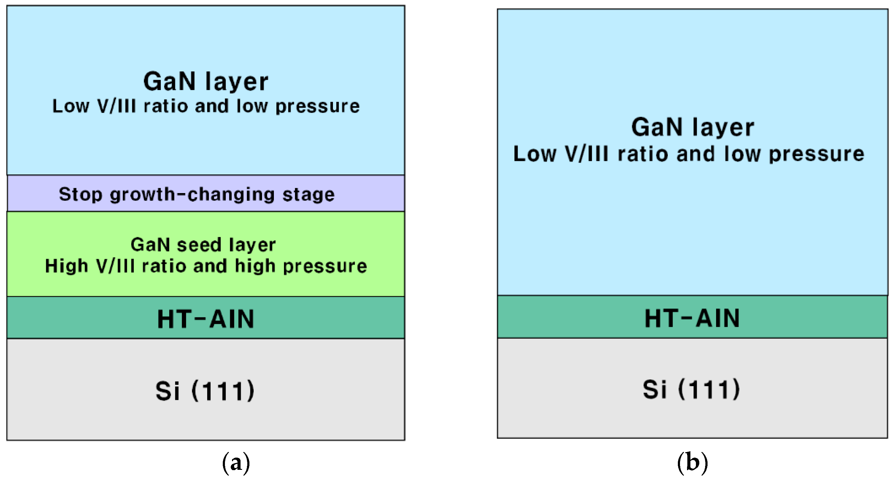
2. Experiments
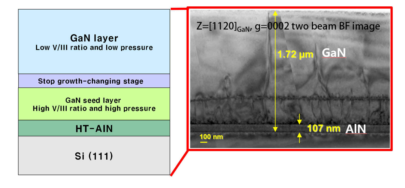
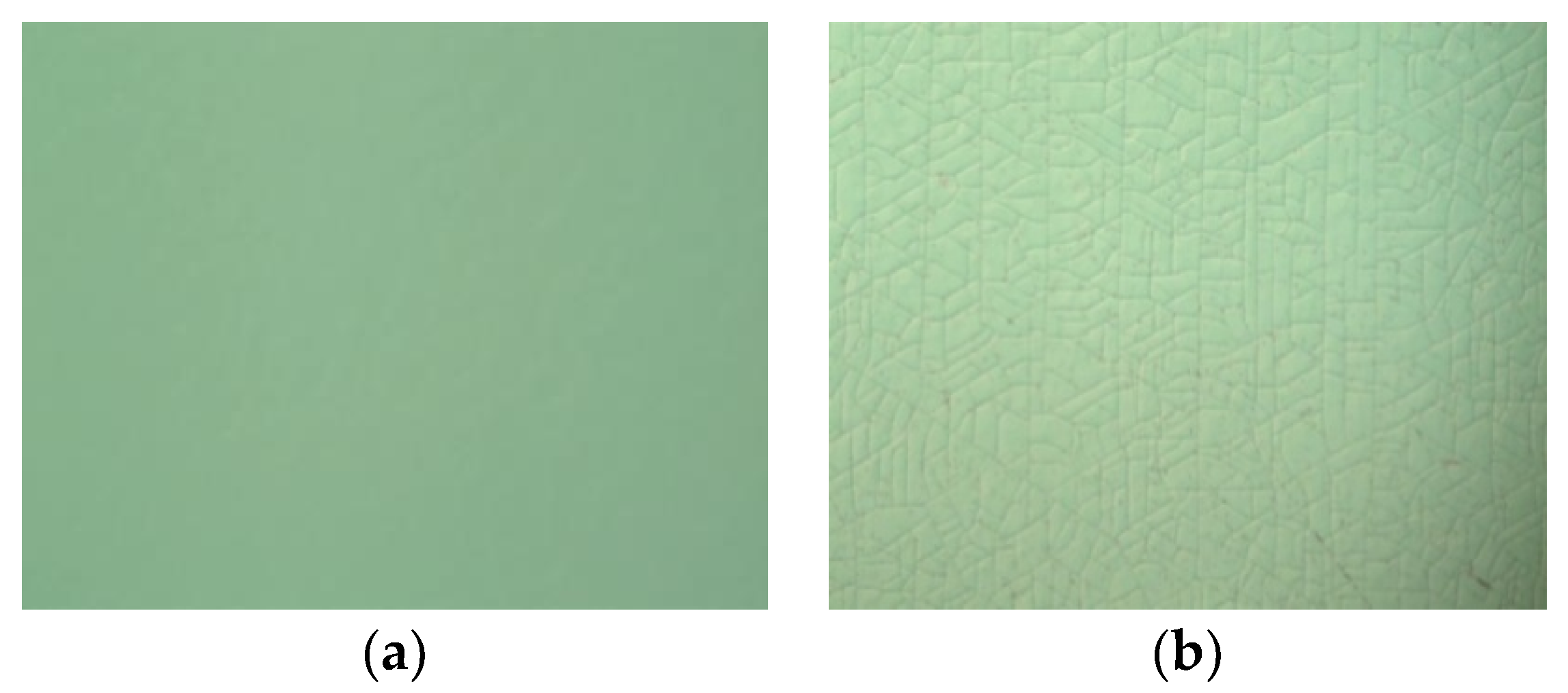
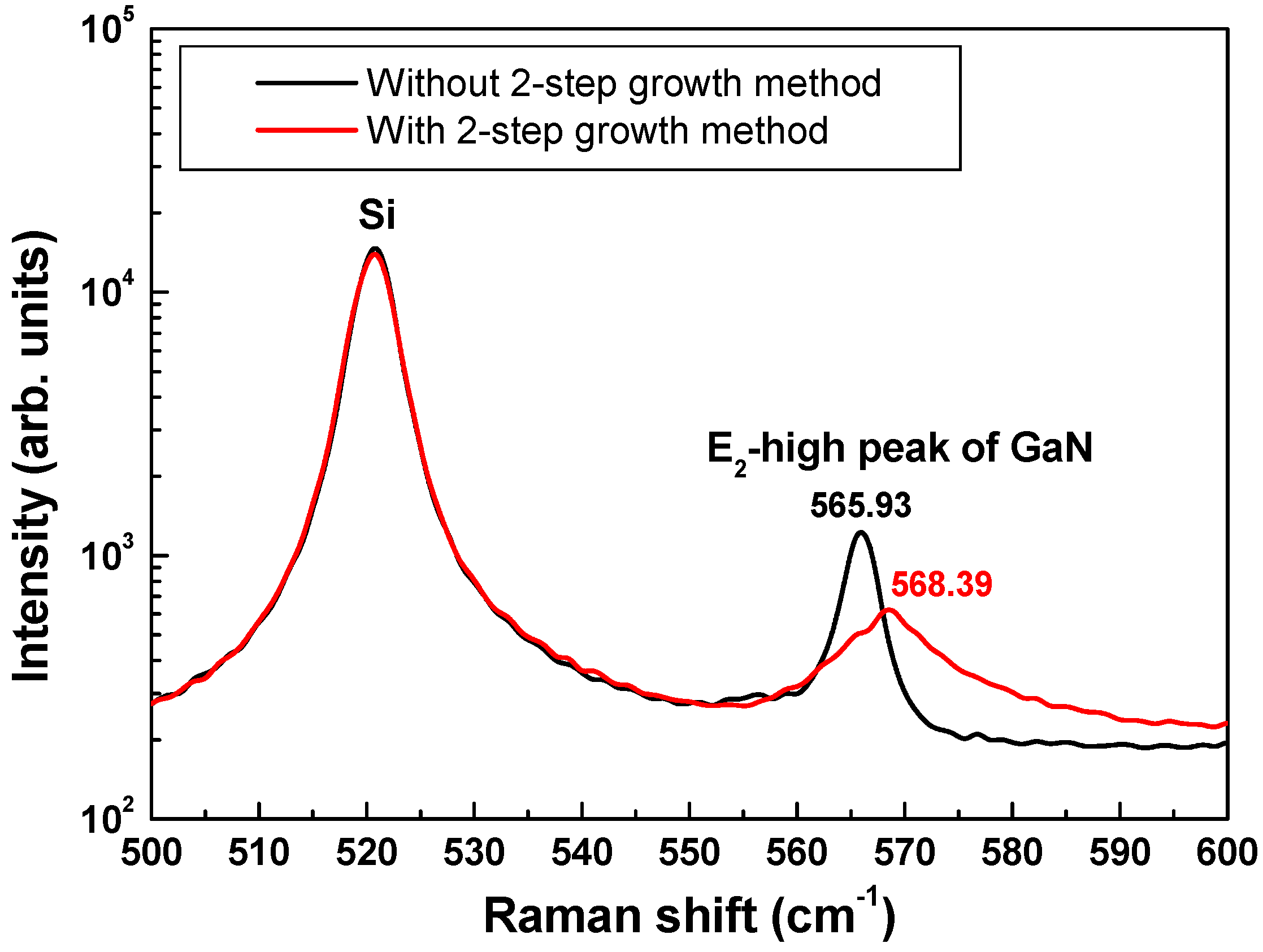
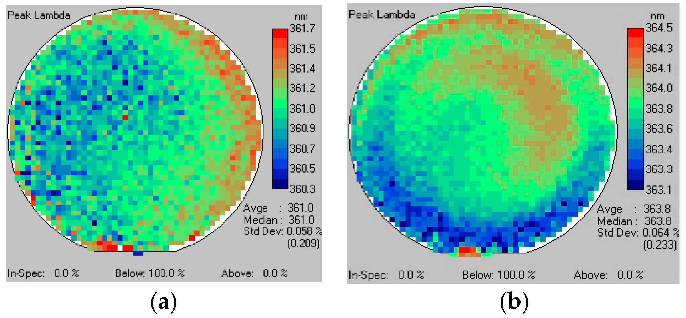
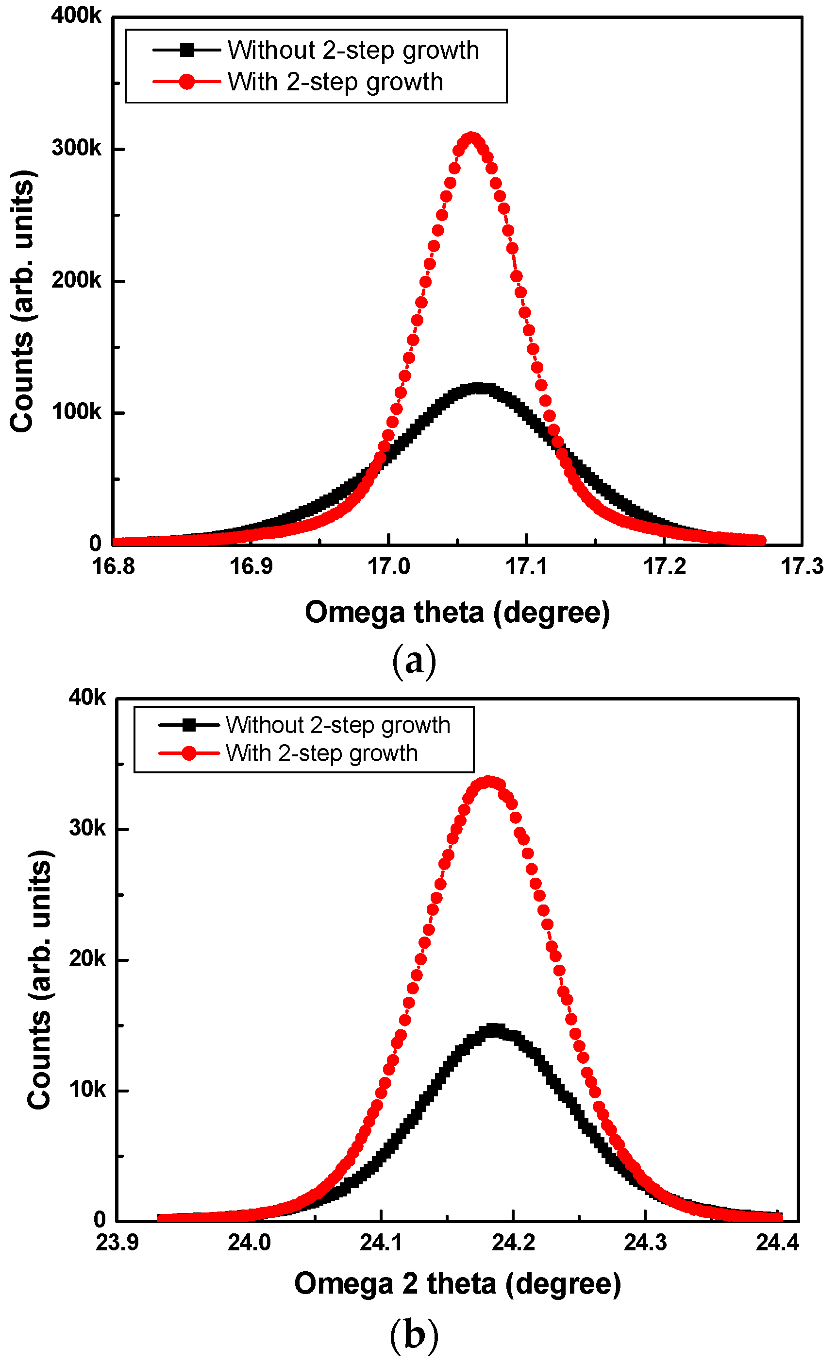
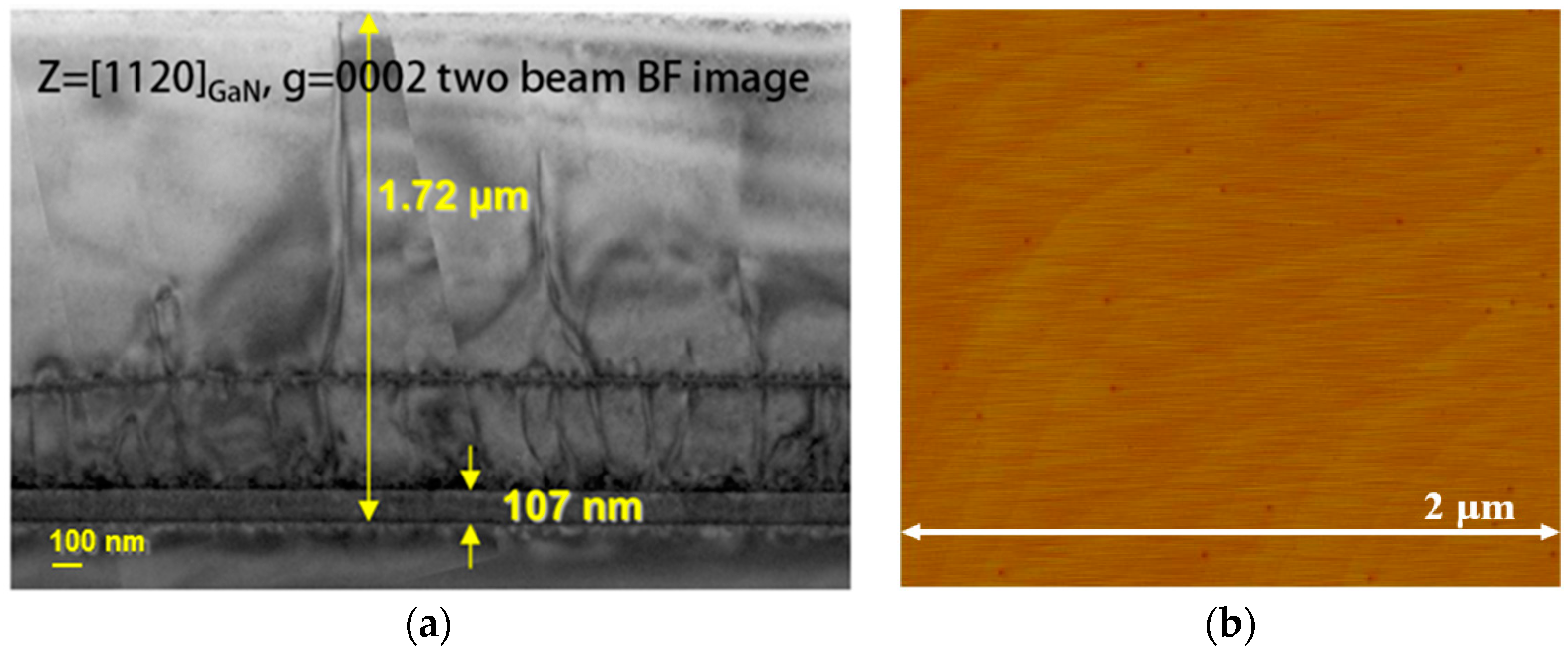
3. Results and Discussion
4. Conclusions
Author Contributions
Funding
Institutional Review Board Statement
Informed Consent Statement
Data Availability Statement
Acknowledgments
Conflicts of Interest
References
- Uemoto, Y.; Hikita, M.; Ueno, H.; Matsuo, H.; Ishida, H.; Yanagihara, M.; Ueda, T.; Tanaka, T.; Ueda, D. Gate injection transistor (GIT)-A normally-off AlGaN/GaN power transistor using conductivity modulation. IEEE Trans. Electron Devices 2007, 54, 3393. [Google Scholar] [CrossRef]
- Lee, J.-H.; Lee, D.Y.; Oh, B.W.; Lee, J.-H. Comparison of InGaN-based LEDs grown on conventional sapphire and cone-shape-patterned sapphire substrate. IEEE Trans. Electron Devices 2010, 57, 157. [Google Scholar] [CrossRef]
- Lee, J.-H.; Lee, J.-H. Abnormal Electrical and Optical Characteristics of InGaN-Based LEDs by Current Stress-Time-Dependent Annihilation. IEEE J. Quantum Electron. 2012, 48, 635. [Google Scholar] [CrossRef]
- Wu, Y.-F.; Kapolnek, D.; Ibbetson, J.P.; Parikh, P.; Keller, B.P.; Mishra, U.K. Very-high power density AlGaN/GaN HEMTs. IEEE Trans. Electron Devices 2001, 48, 586. [Google Scholar]
- Semond, F.; Lorenzini, P.; Grandjean, N.; Massies, J. High electron mobility AlGaN/GaN heterostructures grown on Si(111) by molecular beam epitaxy. Appl. Phys. Lett. 2001, 82, 335. [Google Scholar] [CrossRef]
- Wang, K.; Li, M.D.; Yang, Z.J.; Wu, J.J.; Yu, T.J. Stress control and dislocation reduction in the initial growth of GaN on Si (111) substrates by using a thin GaN transition layer. CrystEngComm 2019, 21, 4792. [Google Scholar] [CrossRef]
- Ma, J.; Zhu, X.; Wong, K.M.; Zou, X.; Lau, K.M. Improved GaN-based LED grown on silicon (111) substrates using stress/dislocation-engineered interlayers. J. Cryt. Growth 2013, 370, 265. [Google Scholar] [CrossRef]
- Cheng, K.; Leys, M.; Degroote, S.; Daele, B.; Boeykens, S.; Derluyn, J.; Germain, M.; Tendeloo, G.; Engelen, J.; Borghs, G. Flat GaN Epitaxial Layers Grown on Si(111) by Metalorganic Vapor Phase Epitaxy Using Step-Graded AlGaN Intermediate Layers. J. Electron. Mater. 2006, 35, 592. [Google Scholar] [CrossRef]
- Egawa, T.; Moku, T.; Ishikawa, H.; Ohtsuka, K.; Jimbo, T. Improved Characteristics of Blue and Green InGaN-Based Light-Emitting Diodes on Si Grown by Metalorganic Chemical Vapor Deposition. Jpn. J. Appl. Phys. 2002, 41, L663. [Google Scholar] [CrossRef]
- Zhang, Y.; Sun, M.; Piedra, D.; Azize, M.; Zhang, X.; Fujishima, T.; Palacios, T. GaN-on-Si Vertical Schottky and p-n Diodes. IEEE Electron Device Lett. 2014, 35, 618. [Google Scholar]
- Khadar, R.A.; Liu, C.; Zhang, L.; Xiang, P.; Cheng, K.; Matioli, E. 820-V GaN-on-Si Quasi-Vertical p-i-n Diodes With BFOM of 2.0 GW/cm2. IEEE Electron Device Lett. 2018, 39, 401. [Google Scholar] [CrossRef]
- Zou, X.; Zhang, X.; Lu, X.; Tang, C.W.; Lau, K.M. Fully Vertical GaN p-i-n Diodes Using GaN-on-Si Epilayers. IEEE Electron Device Lett. 2016, 37, 636. [Google Scholar] [CrossRef]
- Zhang, E.; Yuan, M.; Chowdhury, N.; Cheng, K.; Palacios, T. 720-V/0.35-mcm2 Fully Vertical GaN-on-Si Power Diodes by Selective Removal of Si Substrates and Buffer Layers. IEEE Electron Device Lett. 2018, 39, 715. [Google Scholar] [CrossRef]
- Lee, J.H.; Park, C.; Kim, K.W.; Kim, D.S.; Lee, J.-H. Performance of fully recessed AlGaN/GaN MOSFET prepared on GaN buffer layer grown with AlSiC precoverage on silicon substrate. IEEE Electron Device Lett. 2013, 34, 975. [Google Scholar] [CrossRef]
- Chen, P.; Zhang, R.; Zhao, Z.; Xi, D.; Shen, B.; Chen, Z.; Zhou, Y.; Xie, S.; Lu, W.; Zheng, Y. Growth of high quality GaN layers with AIN buffer on Si(111) substrates. J. Cryst. Growth 2001, 225, 2. [Google Scholar] [CrossRef]
- Lee, J.H.; Lee, J.H.; Cho, H.I. Nitride Based Semiconductor Device and Process for Preparing the Same. U.S. Patent No. 7319064 B2, 15 January 2008. [Google Scholar]
- Tripathy, S.; Chua, S.J.; Chen, P.; Miao, Z.L. Micro-Raman investigation of strain in GaN and AlxGa1−xN/GaN heterostructures grown on Si (111). J. Appl. Phys. 2002, 92, 3503. [Google Scholar] [CrossRef]
- Langea, A.P.; Mahajan, S. Influence of trimethylaluminum predoses on the growth morphology, filmsubstrate interface, and microstructure of MOCVD-grown AlN on (111) Si. J. Cryst. Growth 2019, 511, 106. [Google Scholar] [CrossRef]
- Lee, J.-H.; Lee, M.-B.; Hahm, S.-H.; Lee, Y.-H.; Lee, J.-H.; Bae, Y.-H.; Cho, H.K. Growth of Semi-insulating GaN Layer by Controlling Size of Nucleation Sites for SAW Device Applications. MRS Internet J. Nitride Semicond. Res. 2003, 8, 5. [Google Scholar] [CrossRef]


Publisher’s Note: MDPI stays neutral with regard to jurisdictional claims in published maps and institutional affiliations. |
© 2021 by the authors. Licensee MDPI, Basel, Switzerland. This article is an open access article distributed under the terms and conditions of the Creative Commons Attribution (CC BY) license (http://creativecommons.org/licenses/by/4.0/).
Share and Cite
Lee, J.-H.; Im, K.-S. Growth of High Quality GaN on Si (111) Substrate by Using Two-Step Growth Method for Vertical Power Devices Application. Crystals 2021, 11, 234. https://doi.org/10.3390/cryst11030234
Lee J-H, Im K-S. Growth of High Quality GaN on Si (111) Substrate by Using Two-Step Growth Method for Vertical Power Devices Application. Crystals. 2021; 11(3):234. https://doi.org/10.3390/cryst11030234
Chicago/Turabian StyleLee, Jae-Hoon, and Ki-Sik Im. 2021. "Growth of High Quality GaN on Si (111) Substrate by Using Two-Step Growth Method for Vertical Power Devices Application" Crystals 11, no. 3: 234. https://doi.org/10.3390/cryst11030234
APA StyleLee, J.-H., & Im, K.-S. (2021). Growth of High Quality GaN on Si (111) Substrate by Using Two-Step Growth Method for Vertical Power Devices Application. Crystals, 11(3), 234. https://doi.org/10.3390/cryst11030234