
Numerical Modelling Analysis for Carrier Concentration Level Optimization of CdTe Heterojunction Thin Film–Based Solar Cell with Different Non–Toxic Metal Chalcogenide Buffer Layers Replacements: Using SCAPS–1D Software


Abstract
:1. Introduction
2. Numerical Modeling and Material Parameters
2.1. Numerical Modeling
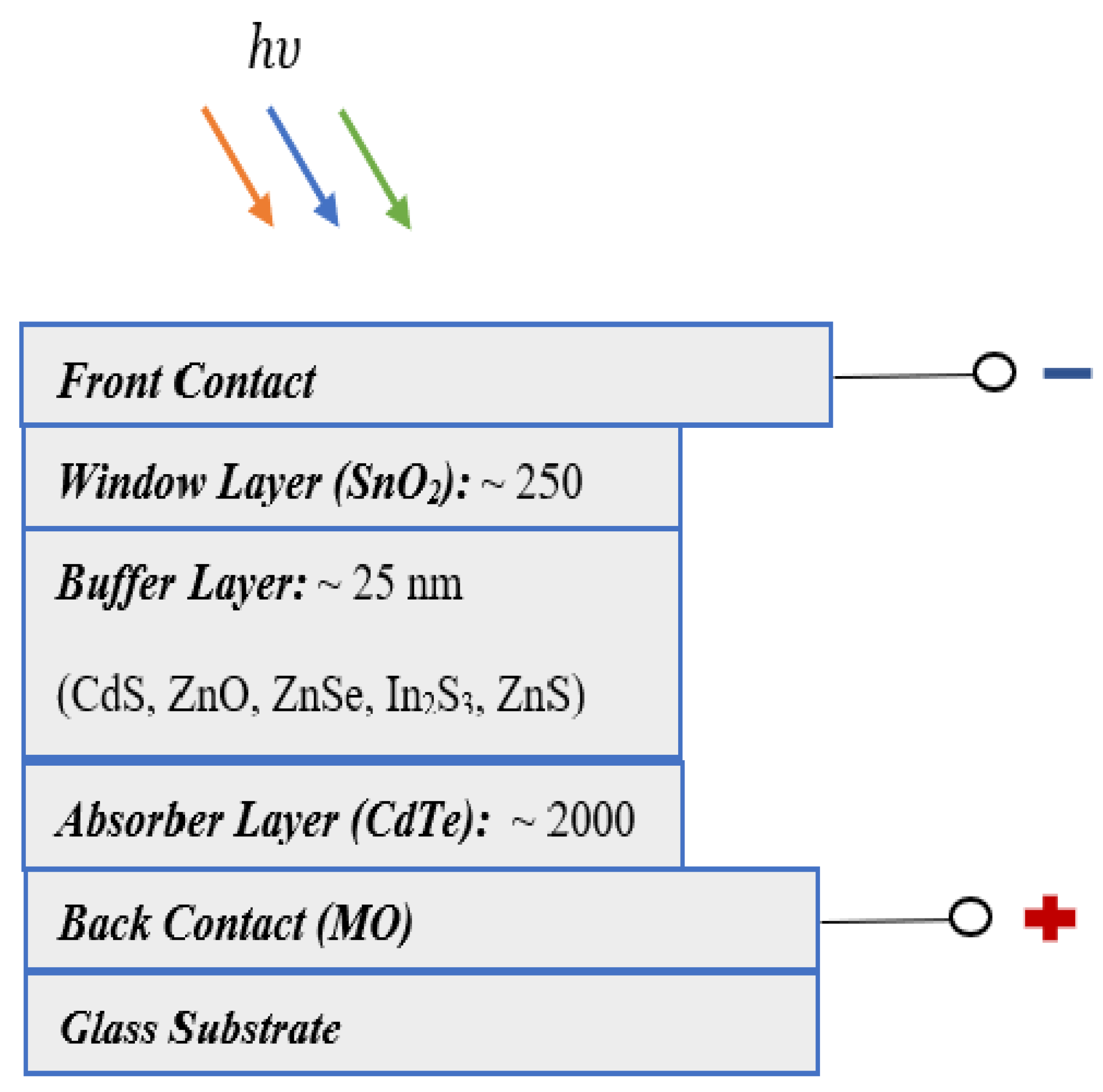
2.2. The Suggested Thin-Film Solar Cell Device Structure
2.3. Numerical Material Parameters
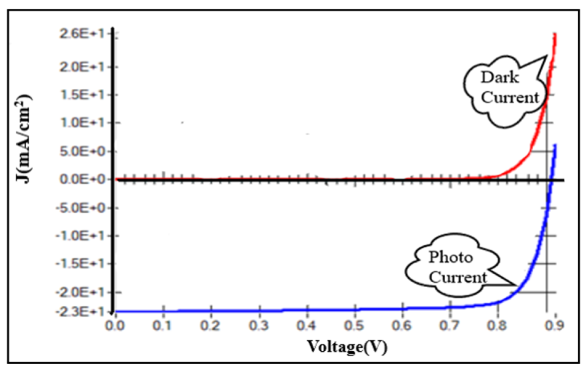
3. Results and Discussion
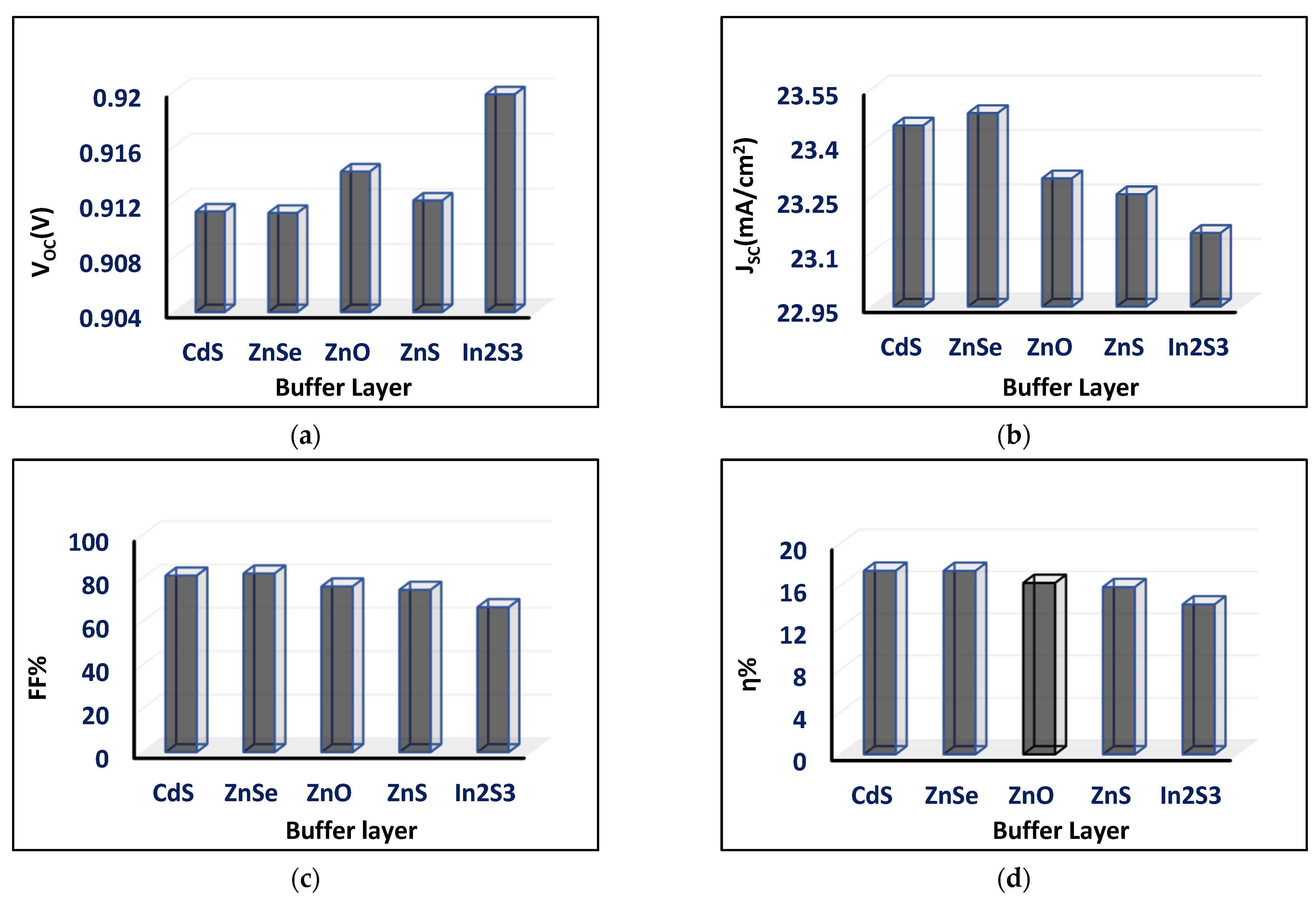
3.1. Effect of Different Buffer Layer on Thin Film-Based Solar Cell
3.2. Modelling and Optimization of CdTe Absorber Layer Doping Level
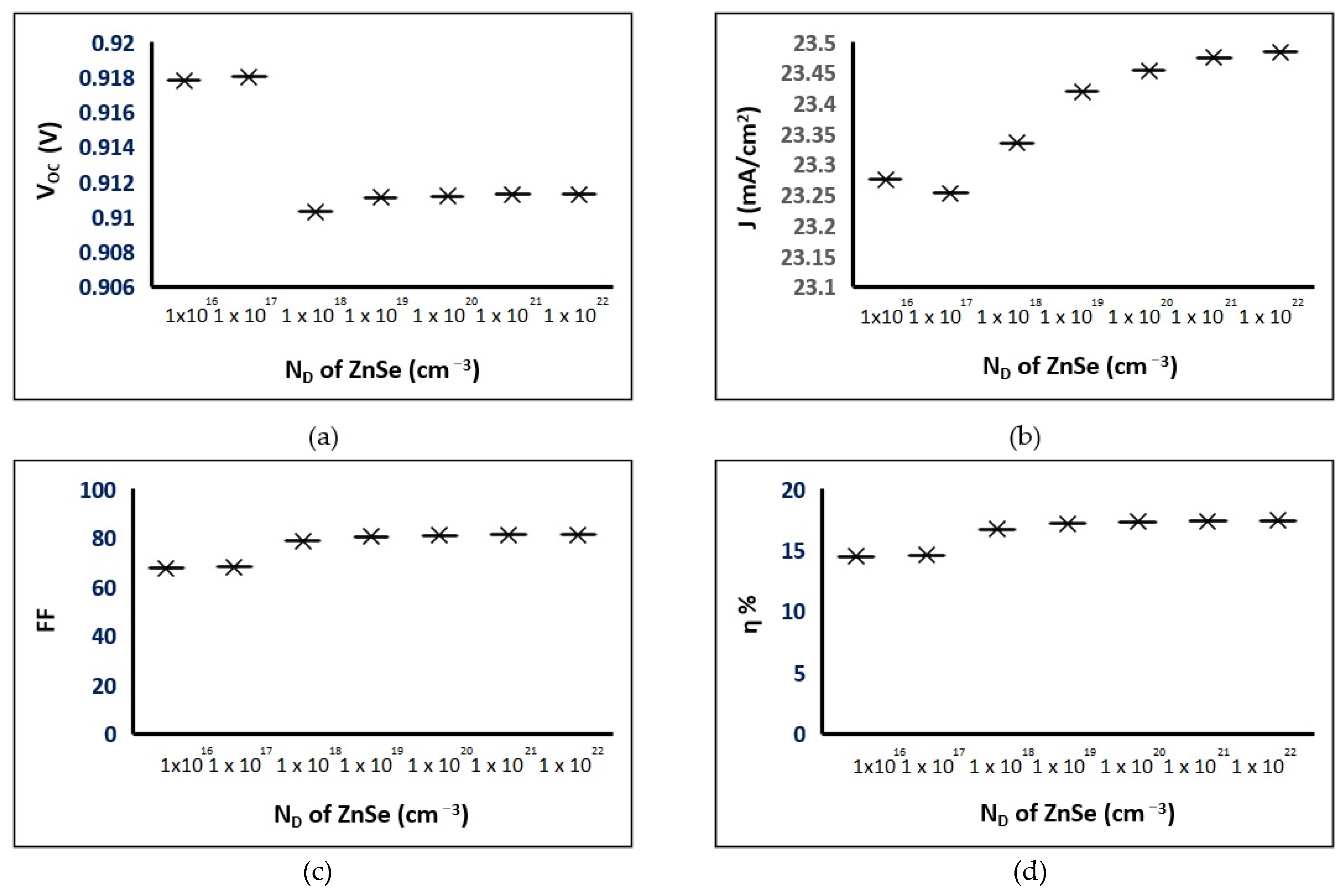
3.3. Modelling and Optimization of ZnSe Buffer Layer Doping Level
3.4. Optimization of the Mo/CdTe/ZnSe/SnO2 Thin Film-Based Solar Cell
3.4.1. Band Diagram
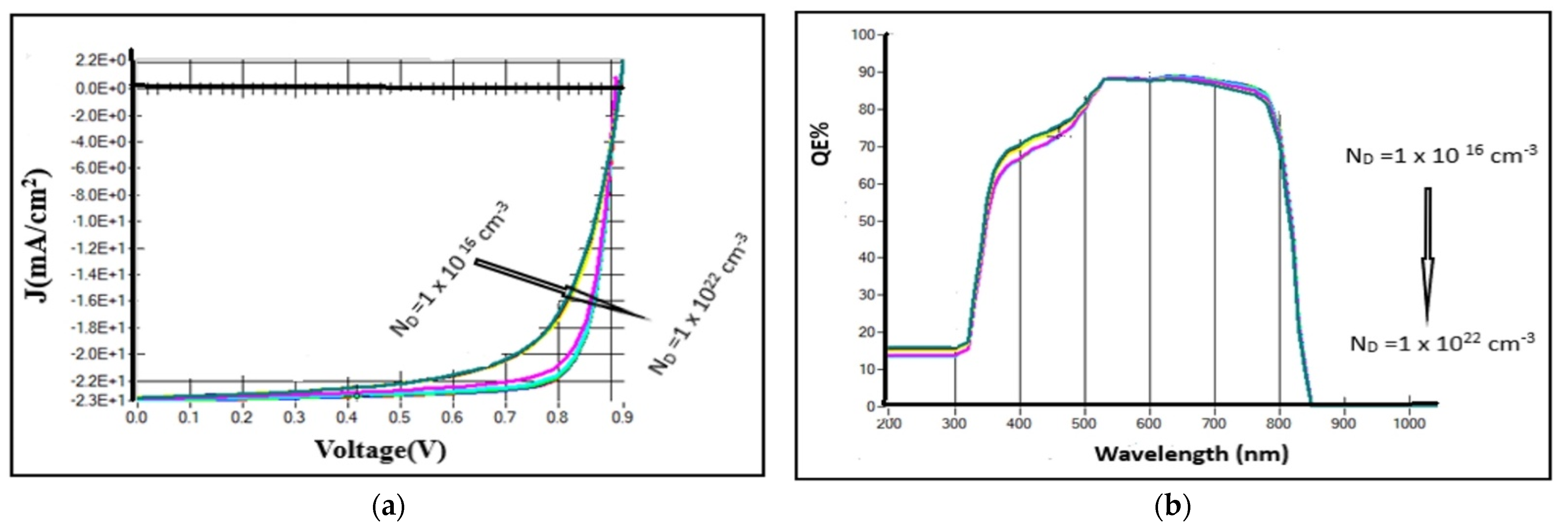
3.4.2. Current Mode
3.4.3. Quantum Efficiency
3.4.4. Effect of Transparent Conducting Layer (Window Layer)
3.5. Comparison between Recent Published Work and Proposed Work
4. Conclusions
Author Contributions
Funding
Acknowledgments
Conflicts of Interest
References
- Kruse, C.N.; Schäfer, S.; Haase, F.; Mertens, V.; Schulte-Huxel, H.; Lim, B.; Min, B.; Dullweber, T.; Peibst, R.; Brendel, R. Simulation–based roadmap for the integration of poly–silicon on oxide contacts into screen–printed crystalline silicon solar cells. Sci. Rep. 2021, 11, 996. [Google Scholar] [CrossRef]
- Zhuk, S.; Kushwaha, A.; Wong, T.K.; Masudy-Panah, S.; Smirnov, A.; Dalapati, G.K. Critical review on sputter–deposited Cu2ZnSnS4 (CZTS) based thin film photovoltaic technology focusing on device architecture and absorber quality on the solar cells performance. Sol. Energy Mater. Sol. Cells 2017, 171, 239–252. [Google Scholar] [CrossRef]
- Najm, A.S.; Ludin, N.A.; Abdullah, M.F.; Almessiere, M.A.; Ahmed, N.M.; Al-Alwani, M.A. Areca catechu extracted natural new sensitizer for dye–sensitized solar cell: Performance evaluation. J. Mater. Sci. Mater. Electron. 2020, 31, 3564–3575. [Google Scholar] [CrossRef]
- Arce-Plaza, A.; Sánchez-Rodriguez, F.; Courel-Piedrahita, M.; Galán, O.V.; Hernandez-Calderon, V.; Ramirez-Velasco, S.; López, M.O. CdTe thin films: Deposition techniques and applications. Coat. Thin Film Technol. 2018, 131–148. [Google Scholar] [CrossRef] [Green Version]
- Gutierrez ZB, K.; Zayas-Bazán, P.G.; De Melo, O.; Moure-Flores, D.; Andraca-Adame, J.A.; Moreno-Ruiz, L.; Martínez-Gutiérrez, H.; Gallardo, S.; Sastré-Hernández, J.; Contreras-Puente, G. CdS/CdTe heterostructures for applications in ultra–thin solar cells. Materials 2018, 11, 1788. [Google Scholar] [CrossRef] [PubMed] [Green Version]
- Maxwell, G.L. Characterization and Modeling of CdCl2 Treated CdTe/CdS Thin-Film Solar Cells; Colorado State University Libraries, Colorado State University: Colorado, CO, USA, 2010. [Google Scholar]
- Kwon, D. Studies of Sputtered Cadmium Telluride and Cadmium Selenide Solar Cells; The University of Toledo: Toledo, OH, USA, 2012. [Google Scholar]
- Hsiao, K.-J. Electron-Reflector Strategy for CdTe Thin-Film Solar Cells. Ph.D. Thesis, Colorado State University, Colorado, CO, USA, 2010. [Google Scholar]
- Emery, K.; Hishikawa, Y.; Warta, W.; Dunlop, E.; Levi, D.; Ho-Baillie, A. Solar cell efficiency tables (Version 46). Mat. Res. Soc. 2015, 23, 231–234. [Google Scholar]
- Bouroushian, M. Electrochemistry of the Chalcogens. In Electrochemistry of Metal Chalcogenides; Springer: Berlin/Heidelberg, Germany, 2010; pp. 57–75. [Google Scholar]
- Belmonte, R.; Angel, M. Quo Vadis Solar Energy Research? Appl. Sci. 2021, 11, 3015. [Google Scholar] [CrossRef]
- Bouloufa, A.; Djessas, K.; Zegadi, A. Numerical simulation of CuInxGa1−xSe2 solar cells by AMPS–1D. Thin Solid Film. 2007, 515, 6285–6287. [Google Scholar] [CrossRef]
- Guo, Y.; Deng, X. Electrodeposition of CdTe thin films and their photoelectrochemical behaviour. Sol. Energy Mater. Sol. Cells 1993, 29, 115–122. [Google Scholar] [CrossRef]
- Su, J.; Minegishi, T.; Katayama, M.; Domen, K. Photoelectrochemical hydrogen evolution from water on a surface modified CdTe thin film electrode under simulated sunlight. J. Mater. Chem. A 2017, 5, 4486–4492. [Google Scholar] [CrossRef]
- Echendu, O.; Okeoma, K.; Oriaku, C.; Dharmadasa, I. Electrochemical deposition of CdTe semiconductor thin films for solar cell application using two–electrode and three–electrode configurations: A comparative study. Adv. Mater. Sci. Eng. 2016, 2016. [Google Scholar] [CrossRef] [Green Version]
- Nikale, V.; Shinde, S.; Bhosale, C.; Rajpure, K. Physical properties of spray deposited CdTe thin films: PEC performance. J. Semicond. 2011, 32, 033001. [Google Scholar] [CrossRef]
- Abdul-Manaf, N.A.; Salim, H.I.; Madugu, M.L.; Olusola, O.I.; Dharmadasa, I.M. Electro–plating and characterisation of CdTe thin films using CdCl2 as the cadmium source. Energies 2015, 8, 10883–10903. [Google Scholar] [CrossRef] [Green Version]
- Salim, H.; Patel, V.; Abbas, A.; Walls, J.; Dharmadasa, I. Electrodeposition of CdTe thin films using nitrate precursor for applications in solar cells. J. Mater. Sci. Mater. Electron. 2015, 26, 3119–3128. [Google Scholar] [CrossRef] [Green Version]
- Ojo, A.; Dharmadasa, I. Analysis of electrodeposited CdTe thin films grown using cadmium chloride precursor for applications in solar cells. J. Mater. Sci. Mater. Electron. 2017, 28, 14110–14120. [Google Scholar] [CrossRef] [Green Version]
- Kwon, Y.; Seo, J.; Kang, Y.; Kim, D.; Kim, J. Bifacial CdS/CdTe thin–film solar cells using a transparent silver nanowire/indium tin oxide back contact. Opt. Express 2018, 26, A30–A38. [Google Scholar] [CrossRef]
- Holi, A.M.; Al-Zahrani, A.A.; Najm, A.S.; Chelvanathan, P.; Amin, N. PbS/CdS/ZnO nanowire arrays: Synthesis, structural, optical, electrical and photoelectrochemical properties. Chem. Phys. Lett. 2020, 750, 137486. [Google Scholar] [CrossRef]
- Najm, A.S.; Chelvanathan, P.; Tiong, S.K.; Ferdaous, M.T.; Shahahmadi, S.A.; Yusoff, Y.; Sopian, K.; Amin, N. Numerical Insights into the Influence of Electrical Properties of n-CdS Buffer Layer on the Performance of SLG/Mo/p-Absorber/n-CdS/n-ZnO/Ag Configured Thin Film Photovoltaic Devices. Coatings 2021, 11, 52. [Google Scholar] [CrossRef]
- Voznyi, A.; Kosyak, V.; Opanasyuk, A.; Tirkusova, N.; Grase, L.; Medvids, A.; Mezinskis, G. Structural and electrical properties of SnS2 thin films. Mater. Chem. Phys. 2016, 173, 52–61. [Google Scholar] [CrossRef] [Green Version]
- Zheng, X.; Li, W.; Aberle, A.G.; Venkataraj, S. Efficiency enhancement of ultra–thin Cu (In, Ga) Se2 solar cells: Optimizing the absorber bandgap profile by numerical device simulations. Curr. Appl. Phys. 2016, 16, 1334–1341. [Google Scholar] [CrossRef]
- Chelvanathan, P.; Yusoff, Y.; Haque, F.; Akhtaruzzaman, M.; Alam, M.; Alothman, Z.; Rashid, M.; Sopian, K.; Amin, N. Growth and characterization of RF-sputtered ZnS thin film deposited at various substrate temperatures for photovoltaic application. Appl. Surf. Sci. 2015, 334, 138–144. [Google Scholar] [CrossRef]
- Ho, W.-H.; Hsu, C.-H.; Yeh, T.-H.; Chang, Y.-H.; Wei, S.-Y.; Lin, T.-Y.; Lai, C.-H. Room–temperature chemical solution treatment for flexible ZnS (O, OH)/Cu (In, Ga) Se2 solar cell: Improvements in interface properties and metastability. ACS Appl. Mater. Interfaces 2016, 8, 6709–6717. [Google Scholar] [CrossRef] [PubMed]
- Abd El Halim, B.; Mahfoud, A.; Elamine, D.M. Numerical analysis of potential buffer layer for Cu2ZnSnS4 (CZTS) solar cells. Optik 2020, 204, 164155. [Google Scholar] [CrossRef]
- Slonopas, A.; Ryan, H.; Foley, B.; Sun, Z.; Sun, K.; Globus, T.; Norris, P. Growth mechanisms and their effects on the opto–electrical properties of CdS thin films prepared by chemical bath deposition. Mater. Sci. Semicond. Process. 2016, 52, 24–31. [Google Scholar] [CrossRef]
- Han, J.; Spanheimer, C.; Haindl, G.; Fu, G.; Krishnakumar, V.; Schaffner, J.; Fan, C.; Zhao, K.; Klein, A.; Jaegermann, W. Optimized chemical bath deposited CdS layers for the improvement of CdTe solar cells. Sol. Energy Mater. Sol. Cells 2011, 95, 816–820. [Google Scholar] [CrossRef]
- Dharmadasa, R.; Lavery, B.; Dharmadasa, I.; Druffel, T. Intense pulsed light treatment of cadmium telluride nanoparticle–based thin films. ACS Appl. Mater. Interfaces 2014, 6, 5034–5040. [Google Scholar] [CrossRef] [PubMed]
- Cai, W.; Feng, L.; Cai, Y.; Zhang, J.; Li, B.; Li, W.; Wu, L.; Lei, Z.; Zheng, J. Produce technology of CdTe thin film modules and design of manufacture line. In Proceedings of the 2006 IEEE 4th World Conference on Photovoltaic Energy Conference, Waikoloa, HI, USA, 7–12 May 2006; pp. 585–587. [Google Scholar]
- Okamoto, T.; Shiina, Y.; Okamoto, S. Investigation of Cu–doping effects in CdTe solar cells by junction photoluminescence with various excitation wavelengths. Jpn. J. Appl. Phys. 2017, 56, 08MC02. [Google Scholar] [CrossRef] [Green Version]
- Okamoto, T.; Hayashi, R.; Ogawa, Y.; Hosono, A.; Doi, M. Fabrication of polycrystalline CdTe thin–film solar cells using carbon electrodes with carbon nanotubes. Jpn. J. Appl. Phys. 2015, 54, 04DR01. [Google Scholar] [CrossRef]
- Jamil, N.Y.; Ivashchenko, M.; Abdulla, S.; Muhammed, A.; Pogrebnjak, A. Design and Fabrication Heterojunction Solarcell of Si-CdS-ZnO Thin Film. In Proceedings of the International Conference Nanomaterials: Applications and Properties; Sumy State University Publishing: Washington, DC, USA, 2012; p. 04NMEEE09. [Google Scholar]
- Zyoud, S.; Zyoud, A. Effect of Absorber (Acceptor) and Buffer (Donor) Layers Thickness on Mo/CdTe/CdS/ITO Thin Film Solar Cell Performance: SCAPS–1D Simulation Aspect. Int. Rev. Model. Simul. (IREMOS) 2021, 14, 10–17. [Google Scholar] [CrossRef]
- Naghavi, N.; Chassaing, E.; Bouttemy, M.; Rocha, G.; Renou, G.; Leite, E.; Etcheberry, A.; Lincot, D. Electrodeposition of In2S3 buffer layer for Cu (In, Ga) Se2 solar cells. Energy Procedia 2011, 10, 155–160. [Google Scholar] [CrossRef] [Green Version]
- Adam, K.B.; Miyauchi, H. Optimization of a Photovoltaic Hybrid Energy Storage System Using Energy Storage Peak Shaving. Int. Rev. Electr. Eng. 2019, 14, 8–18. [Google Scholar] [CrossRef]
- Piarah, W.; Djafar, Z. A New Simulation of Photovoltaic and Thermoelectric Generator Hybrid System with a Beam Splitter Cold and Hot Mirror for Low Intensity. Int. Rev. Mech. Eng. 2019, 13, 559–567. [Google Scholar] [CrossRef]
- Dib, K.; Chenni, R. A Combined MPPT Algorithm for Photovoltaic Systems Based Arduino Microcontroller. Changes 2018, 11, 12. [Google Scholar] [CrossRef]
- Burgelman, M.; Nollet, P.; Degrave, S. Modelling polycrystalline semiconductor solar cells. Thin Solid Film. 2000, 361, 527–532. [Google Scholar] [CrossRef]
- Decock, K.; Khelifi, S.; Burgelman, M. Modelling multivalent defects in thin film solar cells. Thin Solid Film. 2011, 519, 7481–7484. [Google Scholar] [CrossRef]
- Burgelman, M.; Verschraegen, J.; Degrave, S.; Nollet, P. Modeling thin-film PV devices. Prog. Photovolt. Res. Appl. 2004, 12, 143–153. [Google Scholar] [CrossRef]
- Movla, H. Optimization of the CIGS based thin film solar cells: Numerical simulation and analysis. Optik 2014, 125, 67–70. [Google Scholar] [CrossRef]
- Amin, N.; Matin, M.; Aliyu, M.; Alghoul, M.; Karim, M.; Sopian, K. Prospects of back surface field effect in ultra–thin high–efficiency CdS/CdTe solar cells from numerical modeling. Int. J. Photoenergy 2010, 1–8. [Google Scholar] [CrossRef]
- Amin, N.; Yamada, A.; Konagai, M. Effect of ZnTe and CdZnTe Alloys at the Back Contact of 1-µm-Thick CdTe Thin Film Solar Cells. Jpn. J. Appl. Phys. 2002, 41, 2834. [Google Scholar] [CrossRef]
- Aramoto, T.; Kumazawa, S.; Higuchi, H.; Arita, T.; Shibutani, S.; Nishio, T.; Nakajima, J.; Tsuji, M.; Hanafusa, A.; Hibino, T. 16.0% efficient thin–film CdS/CdTe solar cells. Jpn. J. Appl. Phys. 1997, 36, 6304. [Google Scholar] [CrossRef]
- Asaduzzaman, M.; Bahar, A.N.; Bhuiyan, M.M.R. Dataset demonstrating the modeling of a high performance Cu (In, Ga) Se2 absorber based thin film photovoltaic cell. Data Brief 2017, 11, 296. [Google Scholar] [CrossRef] [PubMed]
- Asaduzzaman, M.; Bahar, A.N.; Masum, M.M.; Hasan, M.M. Cadmium free high efficiency Cu2ZnSn (S, Se)4 solar cell with Zn1−xSnxOy buffer layer. Alex. Eng. J. 2017, 56, 225–229. [Google Scholar] [CrossRef]
- Asaduzzaman, M.; Hasan, M.; Bahar, A.N. An investigation into the effects of band gap and doping concentration on Cu (In, Ga) Se2 solar cell efficiency. SpringerPlus 2016, 5, 578. [Google Scholar] [CrossRef] [PubMed] [Green Version]
- Asaduzzaman, M.; Hosen, M.; Ali, M.; Bahar, A.N. Non–toxic buffer layers in flexible Cu (In, Ga) Se2 photovoltaic cell applications with optimized absorber thickness. Int. J. Photoenergy 2017, 1–8. [Google Scholar] [CrossRef] [Green Version]
- Gessert, T.; Sheldon, P.; Li, X.; Dunlavy, D.; Niles, D.; Sasala, R.; Albright, S.; Zadler, B. Studies of ZnTe back contacts to CdS/CdTe solar cells. In Proceedings of the Conference Record of the Twenty Sixth IEEE Photovoltaic Specialists Conference, Anaheim, CA, USA, 29 September–3 October 1997; pp. 419–422. [Google Scholar]
- Hossain, S.; Amin, N.; Martin, M.; Aliyu, M.M.; Razykov, T.; Sopian, K. A numerical study on the prospects of high efficiency ultra thin ZnxCd1−xS/CdTe Solar Cell. Chalcogenide Lett. 2011, 8, 263–272. [Google Scholar]
- Lee, Y.-J.; Gray, J.L. Numerical modeling of polycrystalline CdTe and CIS solar cells. In Proceedings of the Conference Record of the Twenty Third IEEE Photovoltaic Specialists Conference-1993 (Cat. No. 93CH3283-9), Louisville, KY, USA, 10–14 May 1993; pp. 586–591. [Google Scholar]
- Mahabaduge, H.; Rance, W.; Burst, J.; Reese, M.; Meysing, D.; Wolden, C.; Li, J.; Beach, J.; Gessert, T.; Metzger, W. High–efficiency, flexible CdTe solar cells on ultra–thin glass substrates. Appl. Phys. Lett. 2015, 106, 133501. [Google Scholar] [CrossRef]
- Mirkamali, A.S.; Muminov, K.K. Simulation of the efficiency of CdS/CdTe tandem multi–junction solar cells. arXiv 2016, arXiv:1602.01583. [Google Scholar]
- Kotipalli, R.; Poncelet, O.; Li, G.; Zeng, Y.; Francis, L.; Vermang, B.; Flandre, D. Addressing the impact of rear surface passivation mechanisms on ultra–thin Cu (In, Ga) Se2 solar cell performances using SCAPS 1-D model. Sol. Energy 2017, 157, 603–613. [Google Scholar] [CrossRef] [Green Version]
- Limam, N.; Belghachi, A. Analysis of CIGS and CdTe solar cell concentrators. J. Ovonic. Res. Vol. 2017, 13, 129–134. [Google Scholar]
- Jhuma, F.A.; Shaily, M.Z.; Rashid, M.J. Towards high–efficiency CZTS solar cell through buffer layer optimization. Mater. Renew. Sustain. Energy 2019, 8, 6. [Google Scholar] [CrossRef] [Green Version]
- Cozza, D.; Ruiz, C.M.; Duché, D.; Simon, J.J.; Escoubas, L. Modeling the back contact of Cu2ZnSnSe4 solar cells. IEEE J. Photovolt. 2016, 6, 1292–1297. [Google Scholar] [CrossRef]
- Avellaneda, D.; Nair, M.; Nair, P. Cu2SnS3 and Cu4SnS4 thin films via chemical deposition for photovoltaic application. J. Electrochem. Soc. 2010, 157, D346. [Google Scholar] [CrossRef]
- Minbashi, M.; Ghobadi, A.; Ehsani, M.; Dizaji, H.R.; Memarian, N. Simulation of high efficiency SnS-based solar cells with SCAPS. Solar Energy 2018, 176, 520–525. [Google Scholar] [CrossRef]
- Zyoud, S.H.; Zyoud, A.H.; Abdelkader, A.; Ahmed, N.M. Numerical Simulation for Optimization of ZnTe-Based Thin-Film Heterojunction Solar Cells with Different Metal Chalcogenide Buffer Layers Replacements: SCAPS–1D Simulation Program. Int. Rev. Model. Simul. 2021, 14. [Google Scholar] [CrossRef]
- Enam, F.; Rahman, K.; Kamaruzzaman, M.; Sobayel, K.; Chelvanathan, P.; Bais, B.; Akhtaruzzaman, M.; Alamoud, A.; Amin, N. Design prospects of cadmium telluride/silicon (CdTe/Si) tandem solar cells from numerical simulation. Optik 2017, 139, 397–406. [Google Scholar] [CrossRef]
- Kartopu, G.; Oklobia, O.; Turkay, D.; Diercks, D.; Gorman, B.; Barrioz, V.; Campbell, S.; Major, J.; Al Turkestani, M.; Yerci, S. Study of thin film poly–crystalline CdTe solar cells presenting high acceptor concentrations achieved by in–situ arsenic doping. Sol. Energy Mater. Sol. Cells 2019, 194, 259–267. [Google Scholar] [CrossRef]
- Ablekim, T.; Swain, S.K.; Yin, W.-J.; Zaunbrecher, K.; Burst, J.; Barnes, T.M.; Kuciauskas, D.; Wei, S.-H.; Lynn, K.G. Self–compensation in arsenic doping of CdTe. Sci. Rep. 2017, 7, 4563. [Google Scholar] [CrossRef] [PubMed]
- Grover, S.; Li, X.; Zhang, W.; Yu, M.; Xiong, G.; Gloeckler, M.; Malik, R. Characterization of arsenic doped CdTe layers and solar cells. In Proceedings of the 2017 IEEE 44th Photovoltaic Specialist Conference (PVSC), Washington, DC, USA, 25–30 June 2017; pp. 1193–1195. [Google Scholar]
- Kanevce, A.; Reese, M.O.; Barnes, T.; Jensen, S.; Metzger, W. The roles of carrier concentration and interface, bulk and grain–boundary recombination for 25% efficient CdTe solar cells. J. Appl. Phys. 2017, 121, 214506. [Google Scholar] [CrossRef]
- Bailie, C.D.; Christoforo, M.G.; Mailoa, J.P.; Bowring, A.R.; Unger, E.L.; Nguyen, W.H.; Burschka, J.; Pellet, N.; Lee, J.Z.; Grätzel, M. Semi–transparent perovskite solar cells for tandems with silicon and CIGS. Energy Environ. Sci. 2015, 8, 956–963. [Google Scholar] [CrossRef]
- Wang, K.; Gunawan, O.; Todorov, T.; Shin, B.; Chey, S.; Bojarczuk, N.; Mitzi, D.; Guha, S. Thermally evaporated Cu2ZnSnS4 solar cells. Appl. Phys. Lett. 2010, 97, 143508. [Google Scholar] [CrossRef]
- Zhao, W.; Zhou, W.; Miao, X. Numerical simulation of CZTS thin film solar cell. In Proceedings of the 2012 7th IEEE International Conference on Nano/Micro Engineered and Molecular Systems (NEMS), Kyoto, Japan, 5–8 March 2012; pp. 502–505. [Google Scholar]
- Niemegeers, A.; Burgelman, M. Effects of the Au/CdTe back contact on IV and CV characteristics of Au/CdTe/CdS/TCO solar cells. J. Appl. Phys. 1997, 81, 2881–2886. [Google Scholar] [CrossRef]
- Islam, M.M.; Ishizuka, S.; Yamada, A.; Sakurai, K.; Niki, S.; Sakurai, T.; Akimoto, K. CIGS solar cell with MBE-grown ZnS buffer layer. Sol. Energy Mater. Sol. Cells 2009, 93, 970–972. [Google Scholar] [CrossRef]
- Ennaoui, A.; Eisele, W.; Lux-Steiner, M.; Niesen, T.; Karg, F. Highly efficient Cu (Ga, In)(S, Se)2 thin film solar cells with zinc–compound buffer layers. Thin Solid Film 2003, 431, 335–339. [Google Scholar] [CrossRef]
- Spiering, S.; Eicke, A.; Hariskos, D.; Powalla, M.; Naghavi, N.; Lincot, D. Large–area Cd–free CIGS solar modules with In2S3 buffer layer deposited by ALCVD. Thin Solid Film 2004, 451, 562–566. [Google Scholar] [CrossRef]
- Kartopu, G.; Williams, B.L.; Zardetto, V.; Gürlek, A.K.; Clayton, A.J.; Jones, S.; Kessels, W.M.; Creatore, M.; Irvine, S.J. Enhancement of the photocurrent and efficiency of CdTe solar cells suppressing the front contact reflection using a highly–resistive ZnO buffer layer. Sol. Energy Mater. Sol. Cells 2019, 191, 78–82. [Google Scholar] [CrossRef]


| Working Points | Value | Spectrum | AM1.5G Spectrum |
|---|---|---|---|
| Temperature (K) | 300 | Wavelength range (nm) | 200–4000 |
| Bias voltage (V) | 0.00 | Transmission (%) | 100 |
| Frequency (Hz) | 1 × 10⁶ | Ideal light current (mA/cm2) | 20 |
| Series resistance (Ω cm2) | 0 | Transmission of attenuation filter (%) | 100 |
| Shunt resistance (Ω cm2) | 1 × 1030 | Ideal light current cell (mA/cm2) | 0 |
| Electrical Properties | Back Contact | Front Contact | |
|---|---|---|---|
| Thermionic emission surface recombination velocity (cm/s) | Electron | 1 × 10⁷ | 1 × 10⁷ |
| Holes | 1 × 10⁷ | 1 × 10⁷ | |
| Metal work function (eV) | 5 | 4.1 | |
| Majority carrier barrier height (eV) | Relative to EF | 0.4 | 0.1 |
| Relative to EV or EC | −0.1227 | 0.0199 | |
| Allow contact tunneling | Effective mass of electron | 1 | 1 |
| Effective mass of holes | 1 | 1 | |
| Optical Properties | Filter mode | Reflection | Transmission |
| Filter value | 0.8 | 0.95 | |
| Complement of filter value | 0.2 | 0.05 | |
| Electrical Parameter | p–CdTe | n–CdS | n–ZnS | n–ZnSe | n–ZnO | n–In2S3 | SnO2 |
|---|---|---|---|---|---|---|---|
| Thickness (μm) | 2 | 0.025 | 0.025 | 0.025 | 0.025 | 0.025 | 0.25 |
| Band gap (eV) | 1.5 | 2.4 | 3.5 | 2.9 | 3.3 | 2.8 | 3.6 |
| Electron affinity (eV) | 3.9 | 4.5 | 4.5 | 4.09 | 4.45 | 4.7 | 4 |
| Dielectric permittivity (relative) | 9.4 | 10 | 10 | 10 | 9 | 13.5 | 9 |
| CB effective density of states (cm−3) | 8 × 10¹⁷ | 1.5 × 10¹⁸ | 1.5 × 10¹⁸ | 1.5 × 10¹⁸ | 2.2 × 10¹⁸ | 1.8 × 10¹⁹ | 2.2 × 10¹⁸ |
| VB effective density of states (cm−3) | 1.8 × 10¹⁹ | 1.8 × 10¹⁸ | 1.8 × 10¹⁸ | 1.8 × 10¹⁸ | 1.8 × 10¹⁹ | 4 × 10¹⁸ | 1.8 × 10¹⁸ |
| Electron thermal velocity (cm/s) | 1 × 10⁷ | 1 × 10⁷ | 1 × 10⁷ | 1 × 10⁷ | 1 × 10⁷ | 1 × 10⁷ | 1 × 10⁷ |
| Hole thermal velocity (cm/s) | 1 × 10⁷ | 1 × 10⁷ | 1 × 10⁷ | 1 × 10⁷ | 1 × 10⁷ | 1 × 10⁷ | 1 × 10⁷ |
| Electron mobility (cm2/V s) | 300 | 50 | 50 | 50 | 100 | 400 | 100 |
| Hole mobility (cm2/V s) | 40 | 20 | 20 | 20 | 25 | 210 | 25 |
| Shallow uniform donor density ND (cm−3) | 0 | 1 × 10²² | 1 × 10²² | 1 × 10²² | 1 × 10²² | 1 × 10²² | 1 × 10²² |
| Shallow uniform acceptor density NA (cm−3) | 2 × 10¹⁵ | 0 | 0 | 0 | 0 | 0 | 0 |
| Buffer Layer | VOC (V) | JSC (mA/cm2) | FF | Efficiency (%) |
|---|---|---|---|---|
| CdS | 0.9113 | 23.4497335 | 81.41 | 17.43 |
| ZnSe | 0.9112 | 23.484037 | 82.38 | 17.42 |
| ZnO | 0.9142 | 23.303926 | 76.37 | 16.27 |
| ZnS | 0.9121 | 23.260166 | 74.84 | 15.88 |
| In2S3 | 0.9198 | 23.153579 | 66.81 | 14.23 |
| NA (cm−3) | VOC (V) | JSC (mA/cm2) | FF% | η (%) |
|---|---|---|---|---|
| 2 × 10¹² | 0.7333 | 24.249669 | 82.57 | 14.68 |
| 2 × 10¹³ | 0.7398 | 24.248777 | 82.33 | 14.77 |
| 2 × 10¹⁴ | 0.8263 | 24.223452 | 79.49 | 15.91 |
| 2 × 10¹⁵ | 0.9113 | 23.484037 | 81.38 | 17.42 |
| 2 × 10¹⁶ | 0.9662 | 21.748835 | 82.02 | 17.23 |
| 2 × 10¹⁷ | 1.0247 | 19.810091 | 84.21 | 17.09 |
| 2 × 10¹² | 0.7333 | 24.249669 | 82.57 | 14.68 |
| ND (cm−3) | VOC (V) | JSC (mA/cm2) | FF | η (%) |
|---|---|---|---|---|
| 1 × 10¹⁶ | 0.9178 | 23.275532 | 67.70 | 14.46 |
| 1 × 10¹⁷ | 0.918 | 23.25272 | 68.22 | 14.57 |
| 1 × 10¹⁸ | 0.9103 | 23.33507 | 78.62 | 16.70 |
| 1 × 10¹⁹ | 0.9111 | 23.419193 | 80.54 | 17.19 |
| 1 × 10²⁰ | 0.9112 | 23.453013 | 81.07 | 17.33 |
| 1 × 10²¹ | 0.9113 | 23.474864 | 81.29 | 17.39 |
| 1 × 10²² | 0.9113 | 23.484037 | 81.38 | 17.42 |
| Buffer | VOC (V) | JSC (mA/cm2) | FF | η (%) | Ref. | |
|---|---|---|---|---|---|---|
| CdS | Experimental/CBD | 0.69 | 30.9 | 72 | 15.3 | [72] |
| Simulated/SCAPS–1D | 0.9113 | 23.4497335 | 81.41 | 17.43 | This work | |
| ZnSe | Experimental/CBD | 0.67 | 34.9 | 72.7 | 14.4 | [73] |
| Simulated/SCAPS–1D | 0.9112 | 23.484037 | 82.38 | 17.42 | This work | |
| ZnS | Experimental/CBD | 0.55 | 34.4 | 73 | 13.6 | [73] |
| Simulated/SCAPS–1D | 0.9121 | 23.260166 | 74.84 | .88 | This work | |
| In2S3 | Experimental/ALCVD | 0.27 | 46.8 | 71.5 | 12.9 | [74] |
| Simulated/SCAPS–1D | 0.9198 | 23.153579 | 66.81 | 14.23 | This work | |
| ZnO | Experimental/CBD | 0.835 | 24.1 | 75.46 | 15.19 | [75] |
| Simulated/SCAPS–1D | 0.9142 | 23.303926 | 76.37 | 16.27 | This work | |
Publisher’s Note: MDPI stays neutral with regard to jurisdictional claims in published maps and institutional affiliations. |
© 2021 by the authors. Licensee MDPI, Basel, Switzerland. This article is an open access article distributed under the terms and conditions of the Creative Commons Attribution (CC BY) license (https://creativecommons.org/licenses/by/4.0/).
Share and Cite
Zyoud, S.H.; Zyoud, A.H.; Ahmed, N.M.; Abdelkader, A.F.I. Numerical Modelling Analysis for Carrier Concentration Level Optimization of CdTe Heterojunction Thin Film–Based Solar Cell with Different Non–Toxic Metal Chalcogenide Buffer Layers Replacements: Using SCAPS–1D Software. Crystals 2021, 11, 1454. https://doi.org/10.3390/cryst11121454
Zyoud SH, Zyoud AH, Ahmed NM, Abdelkader AFI. Numerical Modelling Analysis for Carrier Concentration Level Optimization of CdTe Heterojunction Thin Film–Based Solar Cell with Different Non–Toxic Metal Chalcogenide Buffer Layers Replacements: Using SCAPS–1D Software. Crystals. 2021; 11(12):1454. https://doi.org/10.3390/cryst11121454
Chicago/Turabian StyleZyoud, Samer H., Ahed H. Zyoud, Naser M. Ahmed, and Atef F. I. Abdelkader. 2021. "Numerical Modelling Analysis for Carrier Concentration Level Optimization of CdTe Heterojunction Thin Film–Based Solar Cell with Different Non–Toxic Metal Chalcogenide Buffer Layers Replacements: Using SCAPS–1D Software" Crystals 11, no. 12: 1454. https://doi.org/10.3390/cryst11121454
APA StyleZyoud, S. H., Zyoud, A. H., Ahmed, N. M., & Abdelkader, A. F. I. (2021). Numerical Modelling Analysis for Carrier Concentration Level Optimization of CdTe Heterojunction Thin Film–Based Solar Cell with Different Non–Toxic Metal Chalcogenide Buffer Layers Replacements: Using SCAPS–1D Software. Crystals, 11(12), 1454. https://doi.org/10.3390/cryst11121454